Article

Resonant Coupling Effects in a Double-Layer THz Bandpass Filter

School of Mechanical Engineering and Automation, Fuzhou University, Fuzhou 350108, China
*
Authors to whom correspondence should be addressed.
Appl. Sci. 2020, 10(15), 5030; https://doi.org/10.3390/app10155030
Submission received: 19 June 2020 / Revised: 13 July 2020 / Accepted: 15 July 2020 / Published: 22 July 2020
(This article belongs to the Section Mechanical Engineering)

Abstract

:

Featured Application

THz bandpass filter design.

Abstract

Cascading similar frequency selective surfaces (FSSs) improves the roll-off rate and frequency selectivity of THz bandpass filters. However, resonant coupling between FSS layers causes anomalous transmission peaks. In this work, we have employed an equivalent circuit model to analyze a double-layer FSS structure with periodic cross apertures at different interlayer spacing. We found that the anomalous peaks can be attributed to the resonant coupling between the upper and lower layer FSSs, and their periodic appearance with changing interlayer spacing is related to the half-wavelength repeatability of the circuit. We have fabricated a double-layer FSS sample using femtosecond laser micromachining and measured it using time-domain THz spectroscopy. The results using the equivalent circuit model agree with the Finite-Difference Time-Domain (FDTD) and experimental results.

1. Introduction

Terahertz (THz) waves generally refer to electromagnetic radiation in the 0.1–10 THz frequency range. THz waves have potential applications in bio-sensing, satellite communication, military radar, object imaging, environmental monitoring, and medical diagnosis [1]. Studies on THz functional devices such as waveguides, polarizers, modulators, antennas, switches, and bandpass filters are particularly important for applications of THz technology [2,3,4,5,6,7,8,9,10,11,12,13]. THz bandpass filters are one of the key components to effectively control and manipulate THz waves. THz filters can be grouped into the following types: photonic crystal filters [7,8], filters based on metamaterials [10,11,12,13], and frequency selective surfaces (FSSs) [14,15,16].
FSS-based filters are composed of periodically arranged apertures on a metal foil. They are easy to fabricate and have a controllable central frequency and a low insertion loss. Most of the commercially available THz bandpass filters are FSS-based. Compared with single-layer FSSs, double-layer FSSs have the characteristics of better frequency selectivity, a higher roll-off rate, and a lower angle sensitivity, suitable for narrowband and multiband operations [17,18,19]. However, periodically appearing anomalous transmission peaks will appear in double-layer stacking when the interlayer spacing and wavelength are of the same order of magnitude [19,20]. What causes these anomalous transmission peaks and their periodic appearance with spacing is important not only in filter design but also for fundamental understanding. Usually, the analysis of this kind of structure relies on the use of commercial full-wave electromagnetic solvers such as the Finite-Difference Time-Domain (FDTD) method. However, it is difficult to understand the physical mechanisms behind the computed transmission spectra of stacked FSS structures. Equivalent circuit models (ECMs) have been utilized to analyze anomalous transmission peaks and show a good agreement with commercial full-wave electromagnetic solvers in the microwave region [21,22,23,24,25].
In this work, we presented a method based on an ECM to examine the THz anomalous transmission phenomena of a double-layer cross FSS structure, and analyzed the evolution and origin of these transmission peaks at different interlayer spacing. We fabricated a double-layer FSS sample using femtosecond laser micromachining and measured it using time-domain THz spectroscopy. The results obtained by the ECM agree with the FDTD and experimental results.

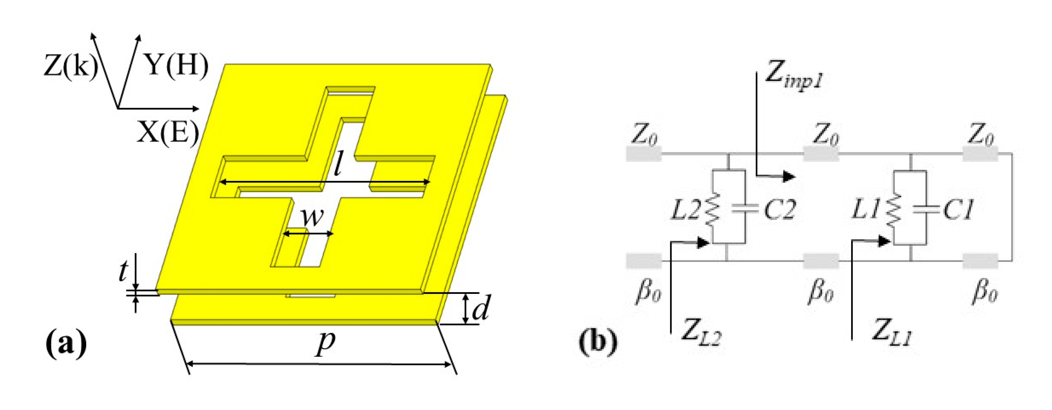
2. Theory and Experiments

The double-layer FSS structure consists of periodically arranged cross apertures perforated on 10 μm Al foils as shown in Figure 1a. Two FSS layers are stacked parallel with no dielectric substrate in between and without lateral shift. Structural parameters of the cross unit include arm length l, arm width w, thickness t, period p, and double-layer spacing d.
The equivalent inductance L and capacitance C are different for FSSs with different shapes and structural parameters. For some commonly used FSS elements, such as rectangles, holes, squares, crosses, etc., the values of L and C can be calculated using theoretical formulas [26,27,28]. However, the accuracy of L and C values obtained using formulas is low, and the error is magnified further after multi-layer stacking. Therefore, we used an inversion method, which employs FDTD (FDTD Solutions, Lumerical Inc., Vancouver, BC, Canada) to calculate the equivalent L and C of the single-layer FSS, in order to concentrate on the coupling effects of the multi-layer stacking. In the FDTD simulation, we used periodic boundary conditions for X and Y directions, and perfect matching layers along the Z direction. The material is Al with a plasma frequency of 2.24 × 10¹⁶ rad/s, and a damping coefficient of 1.12 × 10¹⁴ rad/s. The polarization of the terahertz waves is along the X direction.
Firstly, the transmission coefficient and reflection coefficient of the single-layer FSS were calculated by FDTD. Because the single-layer FSS is a reciprocal symmetric network, we have S12 = S21 (transmission coefficient), S11 = S22 (reflection coefficient). In this way, all the elements in the S matrix of the single-layer FSS can be obtained. Then, the impedance matrix of single-layer FSS was calculated by Equation (1) according to the conversion relationship of the parameters for a two-port network [29,30]:
Z F S S = Z 0 ( 1 + S 11 ) ( 1 S 22 ) + S 12 S 21 ( 1 S 11 ) ( 1 S 22 ) S 12 S 21
where Z0 is the characteristic impedance of free space. For a slot structure, it is equivalent to the inductance L and capacitance C connected in parallel. The admittance can be expressed as
Y F S S = 1 Z F S S = j 2 π f C + 1 j 2 π f L
Assuming that the values of inductance L and capacitance C are stable within the frequency range, by selecting two frequency points f a   and f b in the sub-wavelength region (λ > p) and using Equation (2), the equivalent parameters L and C of the circuit can be calculated as follows:
L = ( f b / f a f a / f b ) j 2 π [ f b Y F S S ( f a ) f a Y F S S ( f b ) ]
C = ( Y F S S ( f a ) / f b Y F S S ( f b ) / f a ) j 2 π ( f a / f b f b / f a )
By cascading the LC oscillation circuits corresponding to the upper and lower layers, we obtained the ECM of the double-layer FSS as shown in Figure 1b. One can see that at Zinp1 port, the electromagnetic wave passes through only one FSS layer and the interlay air. At ZL2 port, the electromagnetic wave has passed through two FSS layers, and ZL2 contains the coupling effect between the two FSS layers. ZL1, Zinp1, and ZL2 in the ECM can be expressed as
Z L 1 = Z 0 × Z F S S Z 0 + Z F S S
Z i n p 1 = Z 0 Z L 1 + j Z 0 t a n ( β 0 × d ) Z 0 + j Z L 1 t a n ( β 0 × d )
Z L 2 = Z i n p 1 × Z F S S Z i n p 1 + Z F S S
where β0 = ω/c, ω is the angular frequency and c is the speed of light in a vacuum. ZL2 obtained from Equation (7) is the load impedance of ECM. The reflection coefficient Γ and the transmittance T of the ECM can be calculated as follows:
Γ = Z L 2 Z 0 Z L 2 + Z 0
T = 1 − Γ2
Single-layer FSSs with geometrical parameters l = 280 μm, w = 65 μm, t = 10 μm, and p = 350 μm were fabricated on 10 μm Al foils using a femtosecond laser micromachining system [13,31]. The femtosecond laser has a wavelength of 800 nm, a pulse width of 45 fs, and a repetition rate of 1 KHz. The Al foil was placed on a computer-controlled two-dimensional translation platform with a moving speed of 500 μm/s and an acceleration of 500 μm/s2, and the laser power used was 10 mW. The calculated focal spot size is 1.44 μm in diameter, and the power density (or irradiance) is about 0.48 MW/cm2.
We stacked two single-layer FSSs to form a double-layer structure. To precisely assemble the two FSS layers, we first put one layer clinging to the other layer (spacing d = 0). We aligned the cross aperture arrays using visible light projection. Then, we moved one filter mounted on a one-dimensional translation stage with respect to the other fixed filter to control the spacing between the two layers. The sample was measured using a home-made time-domain THz spectroscopy system, which employs a Ti: Sapphire femtosecond amplifier and ZnTe crystals for both THz generation and detection. The system has a usable spectral range from 0.2–2.5 THz and a power spectrum dynamic range >50 dB. Time-domain signals were acquired over a time window of about 25 ps, corresponding to a frequency resolution of 40 GHz (Δf = 1/Twindow).

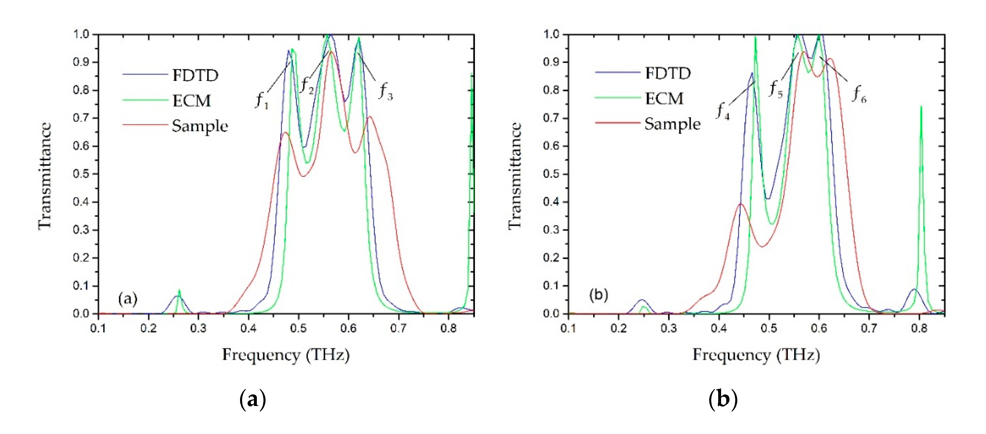
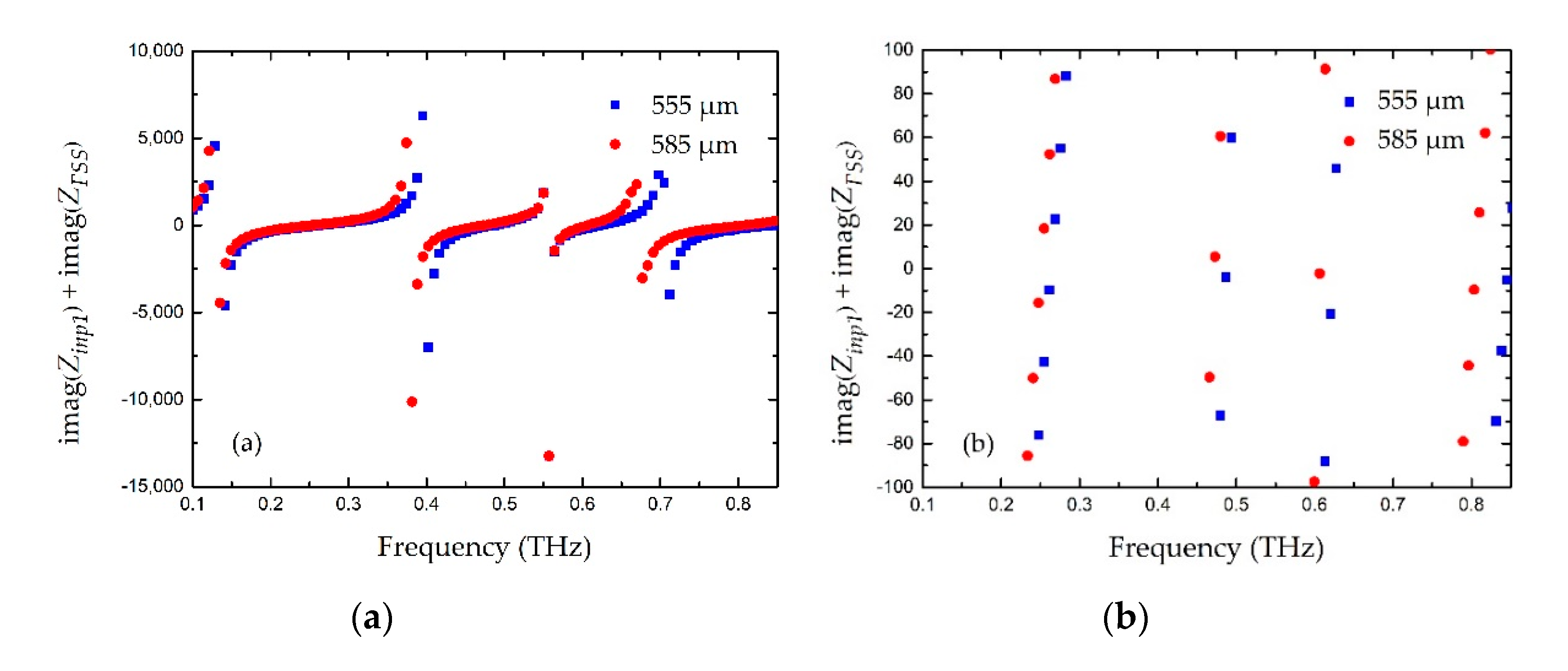
3. Results and Discussion

Figure 2a,b shows the FDTD (blue), ECM (green), and experimental (red) results when the interlayer spacing d equals 555 and 585 μm, respectively. The ECM results are credible only when the calculated wavelength is larger than the period p = 350 μm [24]. The transition point at λp = 350 μm (f = c/λ 0.857 THz) was traditionally referred to as Wood’s anomaly [32]. Thus, the simulation THz range is set from 0.1 to 0.85 THz. In the simulated range, the results obtained by ECM agree with those obtained by FDTD and experiments. We see three peaks in each experimental spectrum, which are labeled as f1, f2, f3 for d = 555 μm and f4, f5, f6 for d = 585 μm. The ECM spectrum shows narrower peaks, because both experiments and FDTD simulations have a limited time window. In the time-domain THz spectroscopy measurements, the time window is confined by the internal reflection pulse of a 1 mm ZnTe detection crystal, appearing at about 21.6 ps after the main THz pulse.
We scanned the interlayer spacing d from 50 to 1050 micron to explore the evolution of the transmission peaks at different interlayer spacing using ECM. We obtained the transmittance contour map for a range from 0.1 to 0.85 THz, as shown in Figure 3a, which coincides with the results of FDTD simulation (Figure 3b). The transmission peak, which does not vary with the spacing d, is highlighted with a white line B, and two transmission lines, periodically appearing like wings on both sides of line B with varying d, are highlighted as line Ai and Ci (i denotes the series of wings).
It can be seen from Figure 2 and Figure 3 that the positions of f2 and f5 coincide with that of line B, at about 0.557 THz. Obviously, the peak highlighted by line B is the intrinsic transmission of the single-layer FSS. In order to analyze the effect of double-layer coupling, we need to look into ZL2. Equation (6) shows that ZL2 is composed of Zinp1 and ZFSS connected in parallel. The air interlayer is represented by Z0 and β0. Zinp1 represents the impedance of the first layer FSS plus interlayer air, and ZFSS represents the equivalent impedance of the second FSS layer.
The single-layer slot-type FSS is equivalent to the parallel connection of inductance and capacitance. When resonance occurs, the inductance reactance and capacitance reactance of the parallel circuit are equal, that is, the inductance current and the capacitance current are equal. Because the inductance current lags behind the voltage by 90° in phase and the capacitance current leads the voltage by 90° in phase, the phase difference between the inductance current and the capacitance current is exactly 180°. At this time, there is no current passing through the circuit (no loss) and the transmittance of the FSS is the maximum.
Similarly, for the double-layer FSS, the total input impedance ZL2 is equivalent to the parallel connection of Zinp1 and ZFSS. As we know, the real part of the impedance represents resistance, while the imaginary part represents reactance. A positive imaginary part represents inductance, while a negative imaginary part represents capacitance. When the transmittance is the maximum, the circuit resonates, and the imaginary parts of the paralleled impedance Zinp1 and ZFSS should be equal in amplitude but with opposite signs. Therefore, we add up the imaginary parts of Zinp1 and ZFSS and plot the sum in Figure 4a for d = 555 μm and d = 585 μm, and Figure 4b is the enlarged view at the sum equal to zero. As it can be seen from the figure, for d = 555 μm, at about 0.487 and 0.621 THz, the sum lines pass zero. At these two zero points, the upper and lower FSSs resonate and the anomalous transmission peaks f1 and f3 appear. For d = 585 μm, at 0.473 and 0.607 THz, the sum lines pass zero, corresponding to the anomalous transmission peaks of f4 and f6. Therefore, according to ECM theory, the anomalous transmission peaks (f1, f3, f4, and f6) can be attributed to the resonant coupling between double FSS layers. At 0.564 THz, that is, the transmission peaks f2 and f5 (also the position of line B), the sum is not equal to zero, because the peak corresponds to the intrinsic transmission of the single-layer FSS and is irrelevant to the double-layer coupling. In addition, the ECM also predicts peaks at about 0.25 and 0.8 THz, which were not observed in our experimental data. For the peak at 0.25 THz, the real part of ZL2 is only about a few ohms, mismatching with the impedance of the free space (377 ohms), indicating a weak resonance/peak. The peak at 0.8 THz is too sharp to be observed in our experiments because we have a limited frequency resolution.
Furthermore, for the periodic appearance of the anomalous transmission peaks/wings, we found that Zinp1 has a certain periodicity. Increasing d by integer multiple of half wavelength ( m λ 2 ) and using Equation (6) to calculate Zinp1 (d+   m λ 2 ), we have
Z i n p 1   ( d + m λ 2 ) = Z 0 Z L 1 + j Z 0 t a n ( β 0 × d + m π ) Z 0 + j Z L 1 t a n ( β 0 × d + m π ) = Z 0 Z L 1 + j Z 0 t a n ( β 0 × d ) Z 0 + j Z L 1 t a n ( β 0 × d ) = Z i n p
This indicates that the impedances of two points with m λ 2 spacing on the transmission line are equal.
We can convert the repetitive phase Δφ = mπ (m is a positive integer) into distance. The repetition period of d is calculated as follows:
Δ d = m c 2 f
By using Equation (11) and substituting different m values, we can plot lines Ai and Ci, which coincide with the center of the periodic wings shown in Figure 3. Therefore, by calculating the sum of the imaginary parts of Zinp1 and ZFSS, we can predict these periodically appearing anomalous transmission peaks/wings that are caused by the resonant coupling between the two FSS layers. Our interpretation is consistent with the explanation in terms of a strongly coupled Fabry–Pérot resonator [21].
In addition, if we draw a horizontal line at a larger spacing d in Figure 3, we obtain more anomalous peaks. They can also be perfectly predicted and explained using our model. At THz frequencies, the thicknesses of commercially available substrates are comparable to the free-space wavelength. Substrates cause unwanted substrate resonances or Fabry–Pérot resonances, which otherwise degrade the transmission characteristics of the cascaded FSS structure, smearing out the anomalous transmission features observed in this work.

4. Conclusions

In this work, we have shown that anomalous THz transmission of a double-layer FSS structure can be explained by ECM. The transmission peak not affected by the layer spacing is attributed to the intrinsic transmission of the single-layer FSS, while the side anomalous transmission peaks are due to the resonant coupling between the equivalent capacitive and inductive reactance of the upper and lower layer FSSs. Their periodic appearance with changing spacing d is associated with the half-wavelength repeatability of the circuit. The ECM results agree with the FDTD and experimental results.

Author Contributions

Data curation, W.Z.; Formal analysis, T.G.; Funding acquisition, F.H. and X.W.; Investigation, X.J. and X.W.; Methodology, T.G. and F.H.; Project administration, F.H.; Software, Y.C.; Validation, Y.C., W.Z., and X.J.; Writing—Original draft, T.G.; Writing—Review and editing, X.W. All authors have read and agreed to the published version of the manuscript.

Funding

This research was funded by the Engineering Research Center for CAD/CAM of Fujian Universities (K201708), and in part by the Guiding Projects of Fujian Science and Technology Department (2019H0005).

Conflicts of Interest

The authors declare no conflict of interest.

References

  1. Mittleman, D.M. Perspective: Terahertz science and technology. J. Appl. Phys. 2017, 122, 230901. [Google Scholar] [CrossRef]
  2. Zangeneh-Nejad, F.; Safian, R. A graphene-based THz ring resonator for label-free sensing. IEEE Sens. J. 2016, 16, 4338–4344. [Google Scholar] [CrossRef]
  3. Zangeneh-Nejad, F.; Safian, R. Hybrid graphene–molybdenum disulphide based ring resonator for label-free sensing. Opt. Commun. 2016, 371, 9–14. [Google Scholar] [CrossRef]
  4. Rahm, M.; Li, J.S.; Padilla, W.J. Thz wave modulators: A brief review on different modulation techniques. J. Infrared Millim. Terahertz Waves 2013, 34, 1–27. [Google Scholar] [CrossRef]
  5. Yarahmadi, M.; Moravvej-Farshi, M.K.; Yousefi, L. Subwavelength graphene-based plasmonic THz switches and logic gates. IEEE Trans. Terahertz Sci. Technol. 2015, 5, 725–731. [Google Scholar] [CrossRef]
  6. Zangeneh-Nejad, F.; Safian, R. Significant enhancement in the efficiency of photoconductive antennas using a hybrid graphene molybdenum disulphide structure. J. Nanophotonics 2016, 10, 036005. [Google Scholar] [CrossRef]
  7. Zangeneh-Nejad, F.; Fleury, R. Topological analog signal processing. Nat. Commun. 2019, 10, 2058. [Google Scholar] [CrossRef]
  8. Zhang, H.; Guo, P.; Chen, P.; Chang, S.; Yuan, J. Liquid-crystal-filled photonic crystal for terahertz switch and filter. J. Opt. Soc. Am. B 2009, 26, 101–106. [Google Scholar] [CrossRef]
  9. He, J.; Liu, P.; He, Y.; Hong, Z. Narrow band-pass tunable terahertz filter based on photonic crystal cavity. Appl. Opt. 2012, 51, 776–779. [Google Scholar] [CrossRef]
  10. Zhou, X.; Yin, X.; Zhang, T.; Chen, L.; Li, X. Ultrabroad terahertz band-pass filter by hyperbolic metamaterial waveguide. Opt. Express 2015, 23, 11657–11664. [Google Scholar] [CrossRef]
  11. Hu, F.; Fan, F.; Zhang, X.; Jiang, W.; Chen, Y.; Li, P.; Yin, X.; Zhang, W. Intensity modulation of a terahertz band-pass filter: Utilizing image currents induced on MEMS reconfigurable metamaterials. Opt. Lett. 2018, 43, 17–20. [Google Scholar] [CrossRef]
  12. Papari, G.P.; Koral, C.; Andreone, A. Geometrical dependence on the onset of surface plasmon polaritons in thz grid metasurfaces. Sci. Rep. 2019, 9, 924. [Google Scholar] [CrossRef] [PubMed] [Green Version]
  13. Papari, G.P.; Nivas, J.J.J.; Koral, C.; Allahyari, E.; Andreone, A. Engineering of high quality factor THz metasurfaces by femtosecond laser ablation. Opt. Laser Technol. 2020, 128, 106159. [Google Scholar] [CrossRef]
  14. Gao, B.; Ren, Z.; Lin, Y.; Chen, Y.; Wang, X. Design and verification of an integrated free-Standing thick-screen FSS radome. IEEE Antennas Wirel. Propag. Lett. 2018, 17, 1630–1634. [Google Scholar] [CrossRef]
  15. Lin, Y.; Yao, H.; Ju, X.; Chen, Y.; Zhong, S.; Wang, X. Free-standing double-layer terahertz band-pass filters fabricated by femtosecond laser micro-machining. Opt. Express 2017, 25, 25125–25134. [Google Scholar] [CrossRef] [PubMed]
  16. Chen, K.; Li, Z.; Liu, J.; Duan, R.; Wang, Y.; Zhang, W.; Cai, B.; Chen, L.; Zhu, Y. A study of FSS in terahertz range for polarization modulation purpose. IEEE Photonics Technol. Lett. 2013, 25, 1613–1615. [Google Scholar] [CrossRef]
  17. Vegesna, S.; Zhu, Y.; Bernussi, A.; Saed, M. Terahertz two-layer FSSs with improved transmission characteristics. IEEE Trans. Terahertz Sci. Technol. 2012, 2, 441–448. [Google Scholar] [CrossRef]
  18. Ebrahimi, A.; Nirantar, S.; Withayachumnankul, W.; Bhaskaran, M. Second-order terahertz bandpass FSS with miniaturized elements. IEEE Trans. Terahertz Sci. Technol. 2015, 5, 761–768. [Google Scholar] [CrossRef]
  19. Rao, L.; Yang, D.; Zhang, L.; Li, T.; Xia, S. Design and experimental verification of terahertz wideband filter based on double-layered metal hole arrays. Appl. Opt. 2012, 51, 912–916. [Google Scholar] [CrossRef]
  20. Miyamaru, F.; Hangyo, M. Anomalous terahertz transmission through double-layer metal hole arrays by coupling of surface plasmon polaritons. Phys. Rev. B 2005, 71, 165408. [Google Scholar] [CrossRef]
  21. Kaipa, C.S.R.; Yakovlev, A.B.; Medina, F.; Mesa, F.; Hibbins, A.P. Circuit modeling of the transmissivity of stacked two-dimensional metallic meshes. Opt. Express 2010, 18, 13309–13320. [Google Scholar] [CrossRef] [PubMed]
  22. Barzegar-Parizi, S. Analysis of stacked structures composed of arrays of thick slits: An accurate analytical circuit model. Plasmonics 2018, 13, 1711–1719. [Google Scholar] [CrossRef]
  23. Molero, C.; Rodríguez-Berral, R.; Mesa, F.; Medina, F. Wideband analytical equivalent circuit for coupled asymmetrical nonaligned slit arrays. Phys. Rev. E 2017, 95, 023303. [Google Scholar] [CrossRef]
  24. Kaipa, C.S.R.; Yakovlev, A.B.; Medina, F.; Mesa, F. Transmission through stacked 2D periodic distributions of square conducting patches. J. Appl. Phys. 2012, 112, 033101. [Google Scholar] [CrossRef] [Green Version]
  25. Costa, F.; Monorchio, A.; Manara, G. An Overview of Equivalent Circuit Modeling Techniques of Frequency Selective Surfaces and Metasurfaces. ACES J. 2014, 29, 960–976. [Google Scholar]
  26. Gao, M.; Abadi, S.; Behdad, N. A dual-band, inductively-coupled miniaturized-element FSS with higher-order bandpass response. IEEE Trans. Antennas Propag. 2016, 64, 3729–3734. [Google Scholar] [CrossRef]
  27. Hokmabadi, M.P.; Wilbert, D.S.; Kung, P.; Kim, S.M. Design and analysis of perfect terahertz metamaterial absorber by a novel dynamic circuit model. Opt. Express 2013, 21, 16455–16465. [Google Scholar] [CrossRef]
  28. Langley, R.J.; Parker, E.A. Equivalent circuit model for arrays of square loops. Electron. Lett. 1982, 18, 294–296. [Google Scholar] [CrossRef]
  29. Pozar, D.M. Microwave Engineering; John Wiley & Sons: New York, NY, USA, 2011; pp. 189–192. [Google Scholar]
  30. Frickey, D.A. Conversions between S, Z, Y, H, ABCD, and T parameters which are valid for complex source and load impedances. IEEE Trans. Microw. Theory Tech. 1994, 42, 205–211. [Google Scholar] [CrossRef]
  31. Chen, Y.Q.; Gao, B.P.; Lin, Y.Z.; Ju, X.W.; Wang, J.; Wang, X.F. Metal wire grid THz polarizer fabricated by femtosecond laser micro-machining. Chin. J. Lasers 2018, 45, 0802005. [Google Scholar] [CrossRef]
  32. Wood, R.W. On a remarkable case of uneven distribution of light in a diffraction grating spectrum. Philos. Mag. 1902, 4, 269–275. [Google Scholar] [CrossRef] [Green Version]
Figure 1. (a) Schematics of the double-layer cross frequency selective surface (FSS) unit structure. l, w, t, p, and d represent the arm length, arm width, thickness, period, and spacing of the double-layer FSS structure, respectively; (b) equivalent circuit model of the double FSS structure.
Applsci 10 05030 g001
Figure 2. Comparison between the experimental, equivalent circuit model (ECM), and Finite-Difference Time-Domain (FDTD) results for spacing d = 555 μm (a) and 585 μm (b).
Applsci 10 05030 g002
Figure 3. (a) The transmittance contour map in a THz range from 0.1 to 0.85 THz for spacing d changing from 50 to 1050 μm, calculated by ECM. Line B highlights the central transmission peak, and line Ai and line Ci highlight the left and right wings, respectively. i denotes the series of wings. (b) The transmittance contour map calculated by FDTD.
Applsci 10 05030 g003
Figure 4. (a) The sum of the imaginary parts of Zinp1 and ZFSS; (b) the enlarged view at the sum equal to zero.
Applsci 10 05030 g004

