Design and Characterization of VHF Band Small Antenna Using CRLH Transmission Line and Non-Foster Matching Circuit

 , and
, and
Abstract
:1. Introduction
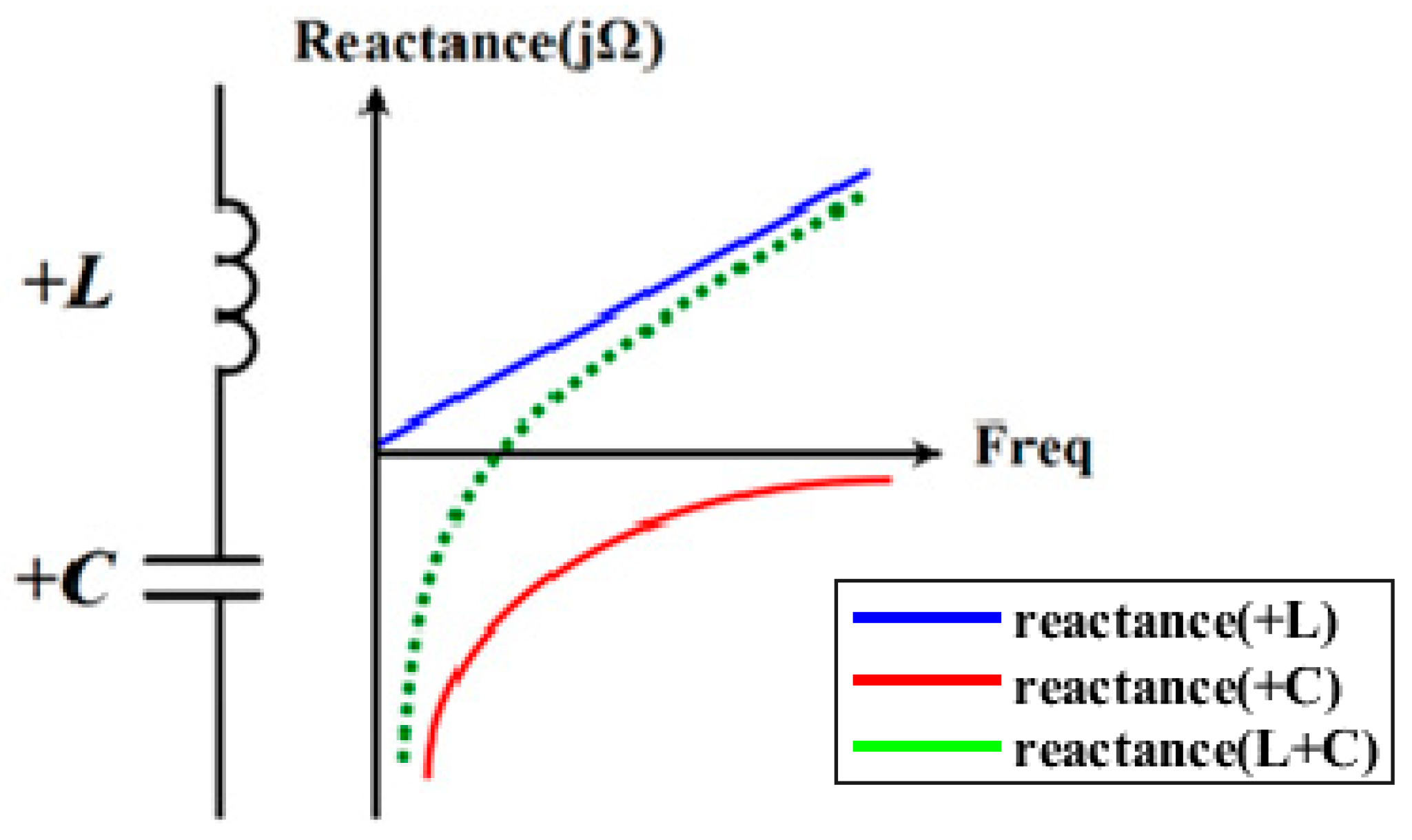
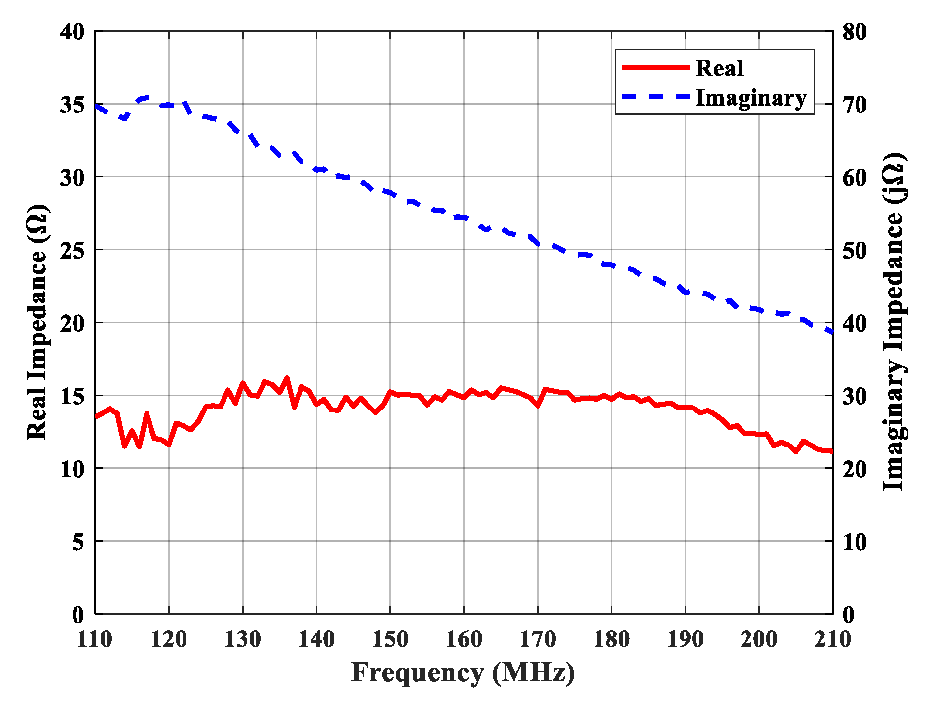
2. Design of Non-Foster Circuit
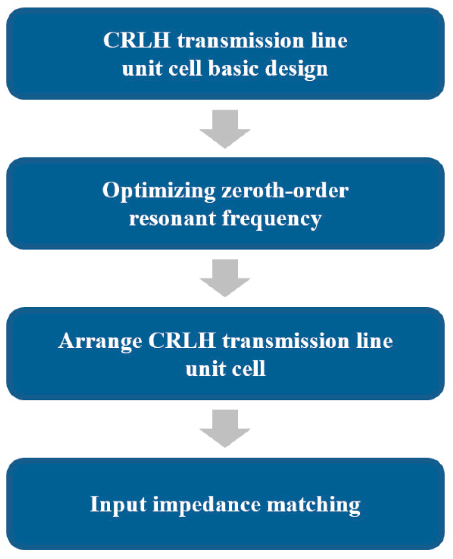
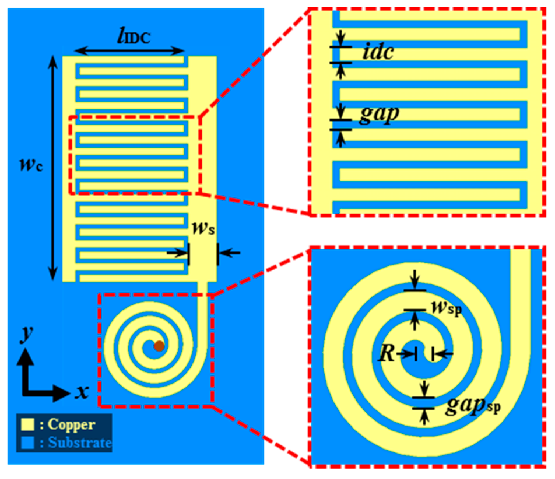
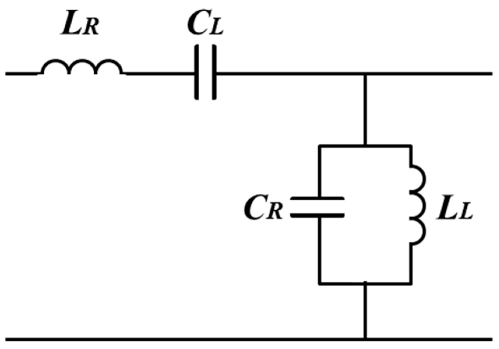
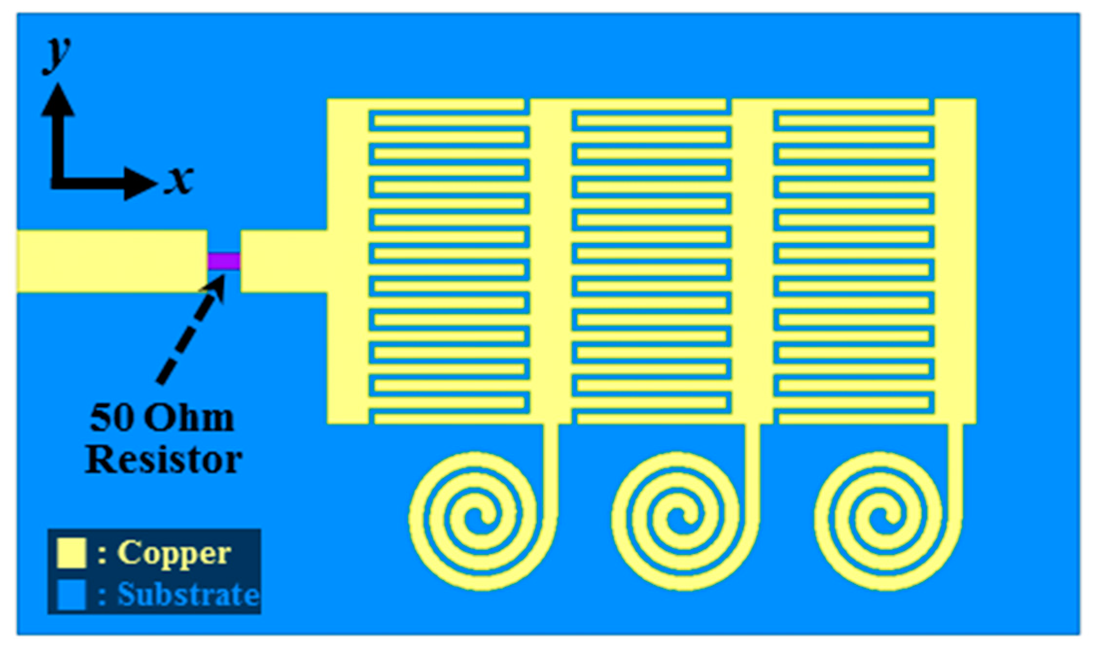
3. Design of CRLH Transmission Line Antenna
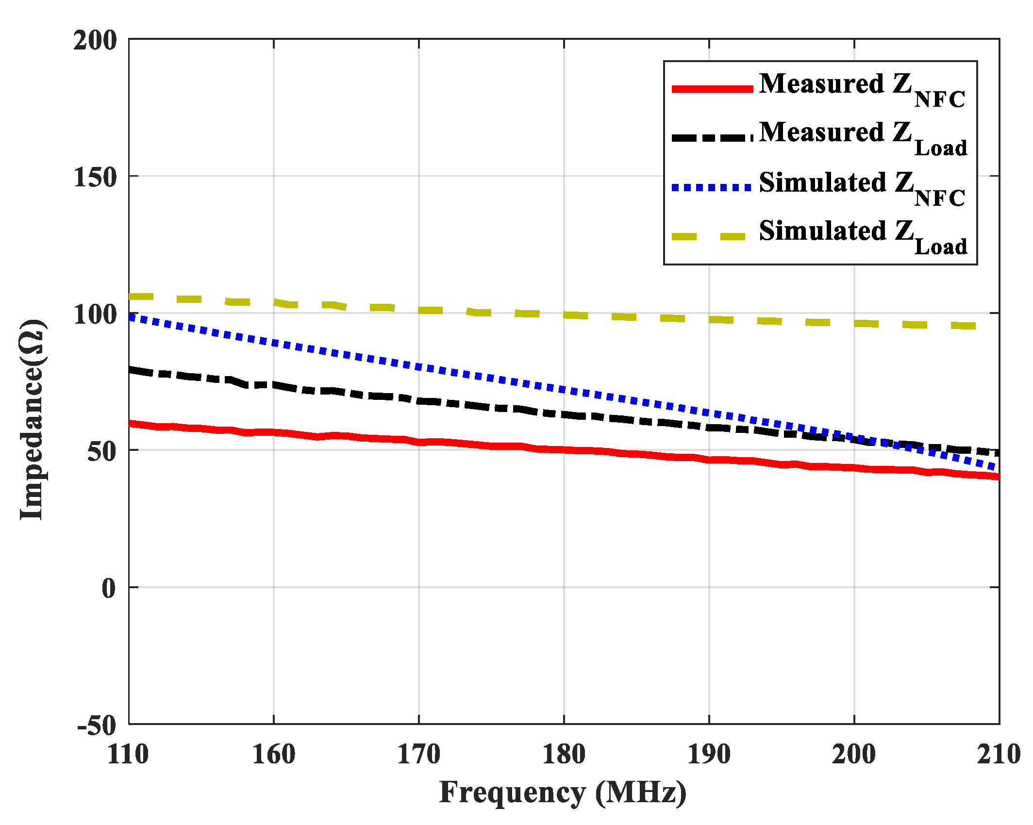
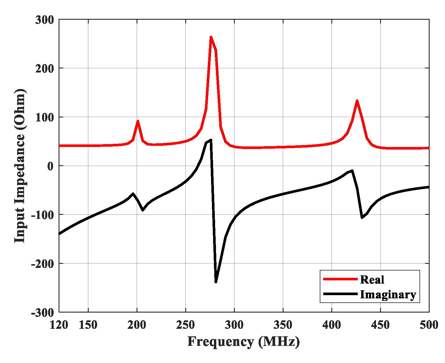
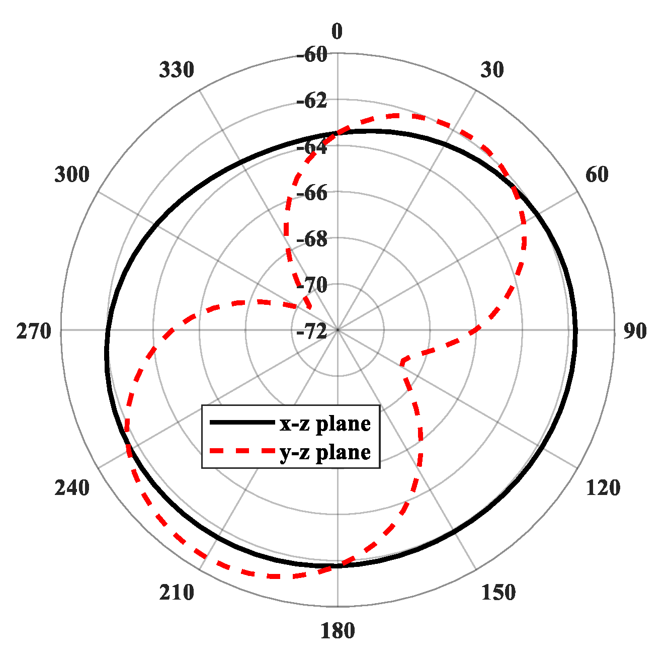
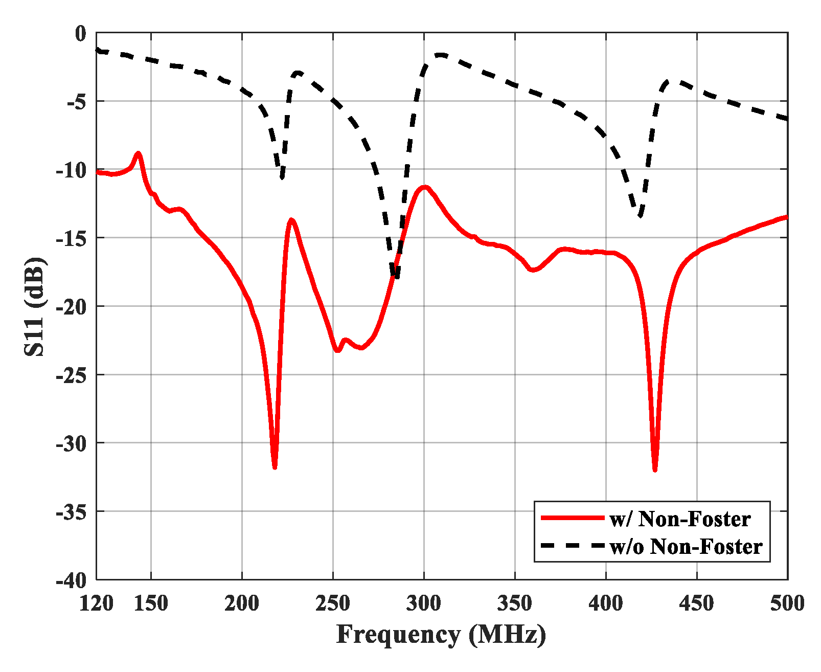
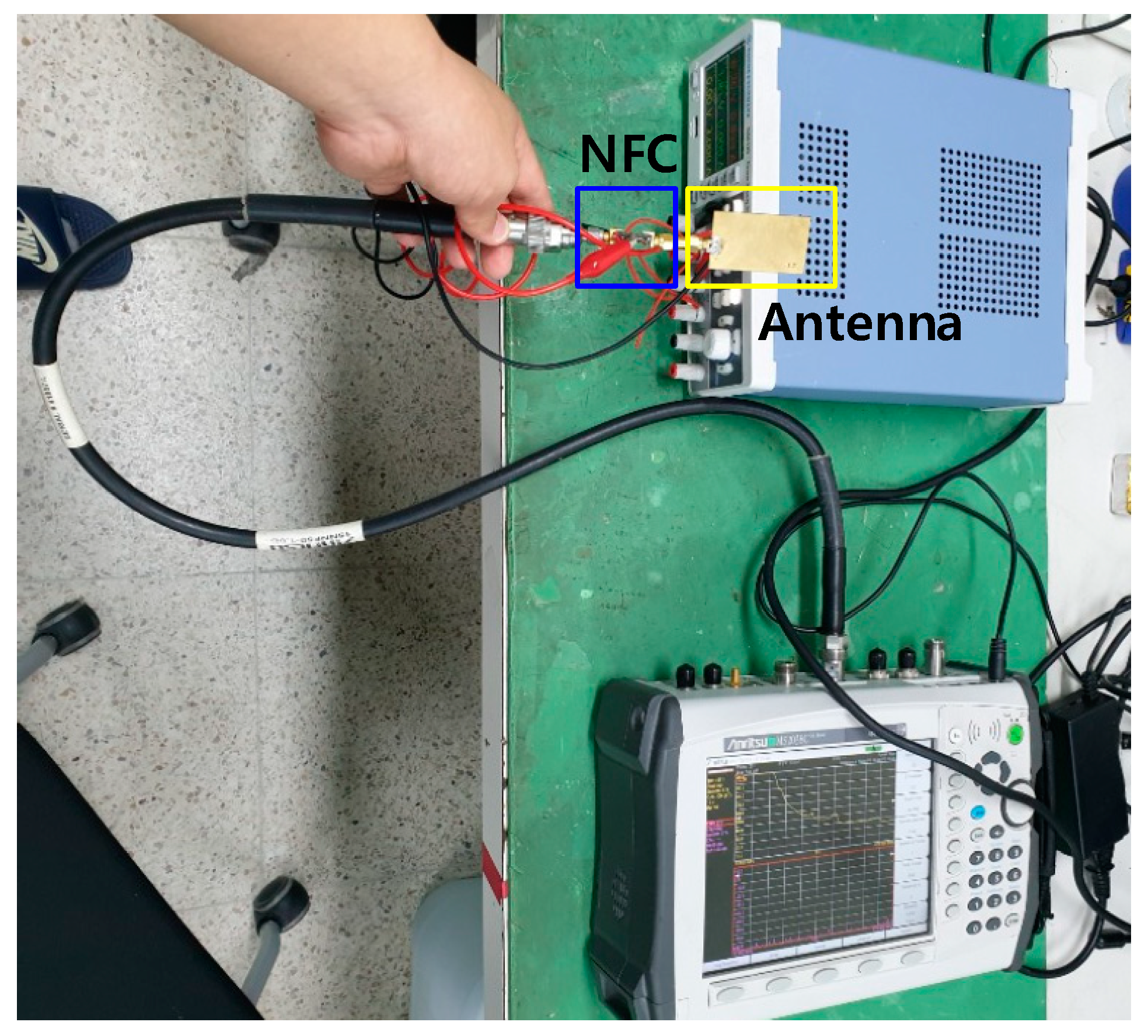
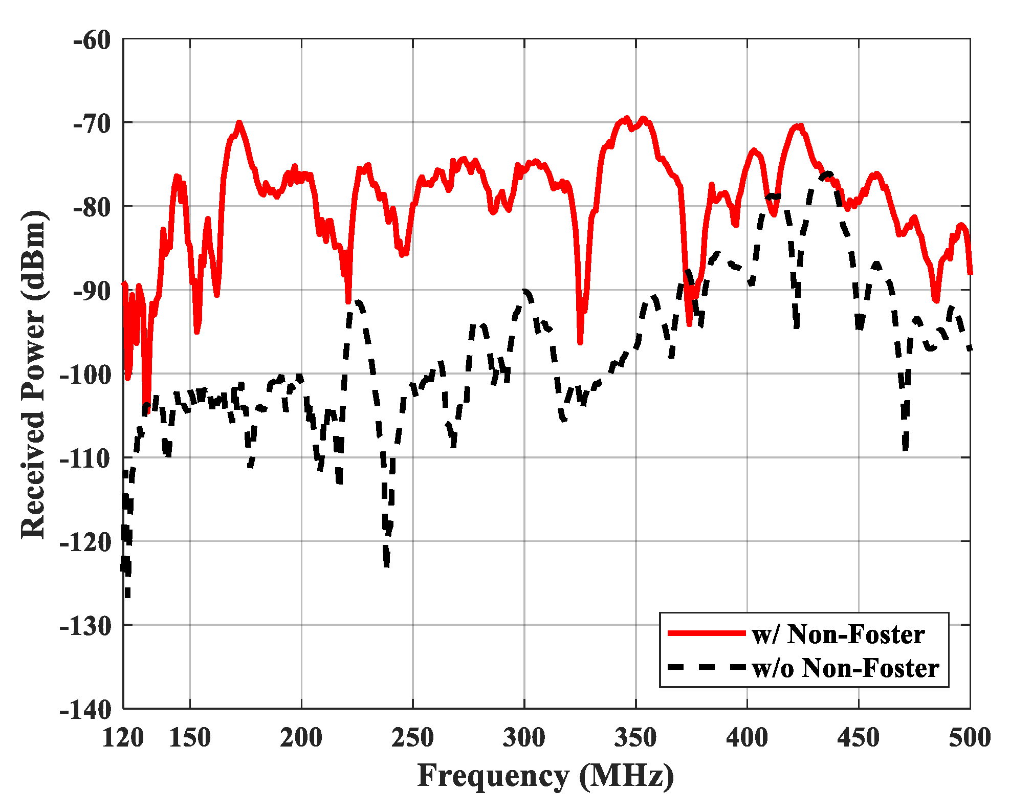
4. Measurement
5. Conclusions
Author Contributions
Funding
Acknowledgments
Conflicts of Interest
References
- Hascall-Denke. Manpack Antenna Products Book. Available online: http://www.hascall-denke.com/product-lines/military-antennas/manpack-antennas/ (accessed on 3 June 2019).
- Hascall-Denke. Vehicular/Marine Antenna Products Book. Available online: http://www.hascall-denke.com/product-lines/military-antennas/marine-antennas/ (accessed on 3 June 2019).
- Lai, A.; Leong, K.M.; Itoh, T. Infinite wavelength resonant antennas with monopolar radiation pattern based on periodic structures. IEEE Trans. Antennas Propag. 2007, 55, 868–876. [Google Scholar] [CrossRef]
- Qureshi, F.; Antoniades, M.A.; Eleftheriades, G.V. A compact and low-profile metamaterial ring antenna with vertical polarization. IEEE Antennas Wirel. Propag. Lett. 2005, 4, 333–336. [Google Scholar] [CrossRef]
- Jang, T.; Choi, J.; Lim, S. Compact coplanar waveguide (CPW)-fed zeroth-order resonant antennas with extended bandwidth and high efficiency on vialess single layer. IEEE Trans. Antennas Propag. 2010, 59, 363–372. [Google Scholar] [CrossRef]
- Ha, J.; Kwon, K.; Choi, J. Compact Zeroth-order Resonance Antenna for Im-plantable Biomedical Service Application. Electron. Lett. 2011, 47, 1267–1269. [Google Scholar] [CrossRef]
- Kim, S.; Lee, J. Frequency and Bandwidth of the Negative/Positive nth Mode of a Composite Right-/Left-Handed Transmission Line. J. Electromagn. Eng. Sci. 2018, 18, 1–6. [Google Scholar] [CrossRef] [Green Version]
- Nelaturi, S.; Sarma, N. A Compact Microstrip Patch Antenna Based on Metamaterials for WiFi and WiMAX Application. J. Electromagn. Eng. Sci. 2018, 18, 182–187. [Google Scholar] [CrossRef] [Green Version]
- Jun, H.J.; Lee, J.; Choi, S.; Park, Y.B. Design and Fabrication of VHF Band Small Antenna Using Composite Right/Left-Handed Transmission Lines. J. Electr. Eng. Technol. 2019, 14, 339–345. [Google Scholar] [CrossRef]
- Alibakhshi-Kenari, M.; Naser-Moghadasi, M.; Sadeghzadeh, R.A. Bandwidth and Radiation Specifications Enhancement of Monopole Antennas Loaded with Split Ring Resonators. IET Microw. Antennas Propag. 2015, 9, 1487–1496. [Google Scholar] [CrossRef]
- Alibakhshi-Kenari, M.; Naser-Moghadasi, M.; Virdee, B.S.; Andújar, A.; Anguera, A. Compact Antenna based on a Composite Right/Left-Handed Transmission Line. Microw. Opt. Technol. Lett. 2015, 57, 1785–1788. [Google Scholar] [CrossRef]
- Alibakhshi-Kenari, M.; Virdee, B.S.; Limiti, E. Compact Single Layer Travelling-Wave Antenna Design Using Metamaterial Transmission-Lines. Radio Sci. 2017, 52, 1510–1521. [Google Scholar] [CrossRef] [Green Version]
- Alibakhshi-Kenari, M.; Virdee, B.S.; Ali, A.; Limiti, E. Miniaturized Planar-Patch Antenna Based on Metamaterial L-shaped Unit-Cells for Broadband Portable Microwave Devices and Multiband Wireless Communication Systems. IET Microw. Antennas Propag. 2018, 12, 1080–1086. [Google Scholar] [CrossRef]
- Alibakhshi-Kenari, M.; Virdee, B.S.; Ali, A.; Limiti, E. Extended Aperture Miniature Antenna Based on CRLH Metamaterials for Wireless Communication Systems Operating Over UHF to C-Band. Radio Sci. 2018, 53, 154–165. [Google Scholar] [CrossRef]
- Saadat, S.; Adnan, M.; Mosallaei, H.; Afshari, E. Composite Metamaterial and Metasurface Integrated with Non-Foster Active Circuit Elements: A Bandwidth-Enhancement Investigation. IEEE Trans. Antennas Propag. 2013, 61, 1210–1218. [Google Scholar] [CrossRef]
- Sussman-Fort, S.E.; Rudish, R.M. Non-Foster impedance matching of electrically-small antennas. IEEE Trans. Antennas Propag. 2009, 57, 2230–2241. [Google Scholar] [CrossRef]
- Go, J.-G.; Chung, J.-Y. Non-Foster Matching Circuit Design to Improve VHF and UHF-Band Small Antenna Impedance Matching. J. Korean Inst. Electromagn. Eng. Sci. 2018, 29, 159–166. [Google Scholar] [CrossRef]
- Ha, S.; Cho, J.; Jung, K. Design of Miniaturized Microstrip Patch Antennas Using Non-Foster Circuits for Compact Controlled Reception Pattern Antenna Array. J. Electromagn. Eng. Sci. 2017, 17, 108–110. [Google Scholar] [CrossRef]
- White, C.R.; Colburn, J.S.; Nagele, R.G. A non-Foster VHF monopole antenna. IEEE Antennas Wirel. Propag. Lett. 2012, 11, 584–587. [Google Scholar] [CrossRef]
- Foster, R.M. A reactance theorem. Bell Syst. Tech. J. 1924, 3, 259–267. [Google Scholar] [CrossRef]
- Long, J. Non-Foster Circuit Loaded Periodic Structures for Broadband Fast and Slow Wave Propagation. Ph.D. Thesis, University of California, San Diego, CA, USA, 2015. [Google Scholar]
- Linvill, J.G. Transistor negative impedance converters. Proc. IRE 1953, 41, 725–729. [Google Scholar] [CrossRef]
- Avago. E-pHEMT ATF-53189 Datasheet. 2013. Available online: https://docs.broadcom.com/doc/AV02-0051EN/ (accessed on 5 June 2019).
- Song, K.S. Non-Foster Impedance Matching and Loading Networks for Electrically Small Antenna. Ph.D. Thesis, The Ohio State University, Columbus, OH, USA, 2011. [Google Scholar]
- Jacob, M.M. Non-Foster Circuit for High Performance Antennas: Advantages and Practical Limitation. Ph.D. Thesis, University of California, San Diego, CA, USA, 2016. [Google Scholar]
- Caloz, C.; Itoh, T. Electromagnetic Metamaterials: Transmission Line Theory and Microwave Applications; Wiley-IEEE Press: New York, NY, USA, 2005. [Google Scholar]
- Kou, N.; Shi, Y.; Li, L. New Equivalent Circuiminiat Analysis and Synthesis for Broadband Composite Right/Left-Handed Transmission Line Metamaterials. ACES J. 2016, 31, 884–893. [Google Scholar]
- Alaris, A. OMNI-A0245 Datasheet. Available online: https://www.Alarisantennas.com/products/passive-monitoring-antenna-2/ (accessed on 5 June 2019).
- Picher, C.; Anguera, J.; Andújar, A.; Borja, C.; Puente, C.; Kahng, S. Reuse of the Mobile Communication Antenna for FM Reception. In Proceedings of the 5th European Conference on Antennas and Propagation (EUCAP), Rome, Italy, 11–15 April 2011; pp. 324–327. [Google Scholar]


| Parameters | Value |
|---|---|
| Zref | 7 pF |
| LG | 0.47 uH |
| LD | 0.47 uH |
| LS | 0.47 uH |
| RG | 1.5 kΩ |
| RD | 1.5 kΩ |
| RS | 1.5 kΩ |
| Rstab | 51 Ω |
| Cstab | 1 pF |
| CG | 510 pF |
| CD | 510 pF |
| Cin | 100 pF |
| Parameters | Value |
|---|---|
| CR | 7.382 pF |
| LL | 19.955 nH |
| CL | 4.177 pF |
| LR | 1.013 nH |
| Parameters | Value |
|---|---|
| wc | 15.7 |
| ws | 2 |
| lIDC | 7.5 |
| idc | 0.5 |
| gap | 0.3 |
| wsp | 0.7 |
| R | 0.5 |
| gapsp | 1 |
| wc | 15.7 |
| ws | 2 |
| Frequency (MHz) | Capacitance (pF) |
|---|---|
| 126 | 9.55 |
| 131 | 9.61 |
| 136 | 9.68 |
| 141 | 9.76 |
| 146 | 9.84 |
| 151 | 9.94 |
| 156 | 10.05 |
| 161 | 10.18 |
| 166 | 10.33 |
| 171 | 10.51 |
| 176 | 10.75 |
| 181 | 11.06 |
| 186 | 11.52 |
| 191 | 12.32 |
| 196 | 14.15 |
| Reference | Antenna Size | Bandwidth | Substrate |
|---|---|---|---|
| 2015 [10] | 22 × 30 × 0.8 mm3 0.21λ0 × 0.29λ0 × 0.008λ0 @2.9 GHz | 4 GHz (2.6–6.6 GHz) 87% | Duroid 5880 |
| 2015 [11] | 20.4 × 6.8 × 0.8 mm3 0.39λ0 × 0.13λ0 × 0.015λ0 @5.8 GHz | 1.5 GHz (5.8–7.3 GHz) 23% | RO4003 |
| 2017 [12] | 21.5 × 30 × 0.8 mm3 0.372λ0 × 0.52λ0 × 0.014λ0 @5.2 GHz | 6.8 GHz (1.8–8.6 GHz) 120% | RO4003 |
| 2018 [13] | 23 × 17 × 1.6 mm3 0.037λ0 × 0.027λ0 × 0.0026λ0 @0.48 GHz | 6.02 GHz (0.48–6.5 GHz) 172.49% | Duroid 5880 |
| 2018 [14] | 17.5 × 32.15 × 1.6 mm3 0.204λ0 × 0.375λ0 × 0.018λ0 @3.5 GHz | 7.05 GHz (0.85–7.9 GHz) 161.14% | FR-4 |
| proposed antenna | 31.4 × 23.7 × 1.6 mm3 0.014λ0 × 0.01λ0 × 0.0007λ0 @0.14 GHz | 0.153GHz (0.14–293 GHz) 70.3% | FR-4 |
© 2020 by the authors. Licensee MDPI, Basel, Switzerland. This article is an open access article distributed under the terms and conditions of the Creative Commons Attribution (CC BY) license (http://creativecommons.org/licenses/by/4.0/).
Share and Cite
Lee, S.; Lee, J.; Choi, S.; Lee, Y.-H.; Chung, J.-Y.; Hwang, K.C.; Park, Y.B. Design and Characterization of VHF Band Small Antenna Using CRLH Transmission Line and Non-Foster Matching Circuit. Appl. Sci. 2020, 10, 6366. https://doi.org/10.3390/app10186366
Lee S, Lee J, Choi S, Lee Y-H, Chung J-Y, Hwang KC, Park YB. Design and Characterization of VHF Band Small Antenna Using CRLH Transmission Line and Non-Foster Matching Circuit. Applied Sciences. 2020; 10(18):6366. https://doi.org/10.3390/app10186366
Chicago/Turabian StyleLee, Soyeong, Jonghyup Lee, Seongro Choi, Yong-Hyeok Lee, Jae-Young Chung, Keum Cheol Hwang, and Yong Bae Park. 2020. "Design and Characterization of VHF Band Small Antenna Using CRLH Transmission Line and Non-Foster Matching Circuit" Applied Sciences 10, no. 18: 6366. https://doi.org/10.3390/app10186366
APA StyleLee, S., Lee, J., Choi, S., Lee, Y.-H., Chung, J.-Y., Hwang, K. C., & Park, Y. B. (2020). Design and Characterization of VHF Band Small Antenna Using CRLH Transmission Line and Non-Foster Matching Circuit. Applied Sciences, 10(18), 6366. https://doi.org/10.3390/app10186366