Abstract
A method applied for improving the measurement precision and efficiency of wafer focusing in an optical lithography instrument (OLI) is introduced. Based on grating shearing interferometry, the defocus and tilt of the wafer are measured by testing the phase difference in the interference pattern. To validate the feasibility, an experiment is implemented, of which the measurement precision is indicated as 30 nm due to the high precision of phase-resolving arithmetic after analyzing the measurement uncertainty and indicating the precision by interferometer.
1. Introduction
The wafer focusing technique (WFT) [1,2] is a pivotal section in optical lithography instruments (OLIs) [3], which affects the image quality and exposure effect [4]. In traditional OLIs, charge coupled device (CCD) sensors [5] and position sensitive detectors (PSDs) [6] are applied and wafer defocus with micron precision is measured by analyzing the image removement of the gap in the WFT system based on a triangle method.
With the improvement of the exposure field of view (FOV) and resolution in new-fashioned OLI [7], the WFT needs higher measurement precision and thus the WFT is widely investigated [8,9]. Based on the Talbot-moiré effect [10] and interferometric spatial-phase imaging [11], a diffractive grating [12,13] is applied for wafer defocus measurement to improve the precision; another technique based on a probe beam scanner [14,15] is also introduced. By complicated analyzation and calculation, these two WFTs have nanometer measurement precision.
To improving the measurement efficiency of WFT with nanometer measurement precision, a simple WFT based on grating shearing interferometry is proposed in this paper. The defocus of the wafer is immediately detected by measuring the phase difference in the interference pattern at meridian position through the measurement system, which is simply composed of a diffractive grating and a CCD sensor. Like traditional grating interferometry [16,17], the advantages of grating shearing interferometry are its high precision and simple setup, while its calculation is complex. This paper proposes a spatial domain phase shift technique for calculating the phase difference in the interferometry fringe between the focus and defocus positions of the wafer.
In summary, a novel WFT based on grating shearing interferometry and a spatial domain phase shift technique is introduced to improve the measuring precision and efficiency. An experiment is carried out to verify the feasibility and calibrate the measurement precision of this technology in this paper.
2. Methodology
The measurement system for the WFT introduced in this paper is simply composed of a laser, beam expander and collimator, 4f optical lenses, a diffractive grating and CCD (charge coupled device), as shown in Figure 1.
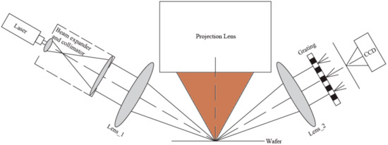
Figure 1.
Illustration of focus measurement system (CCD: charge coupled device).
The plane wavefront formed by the beam expander and collimator is transformed by lenses and sheared by the diffractive grating. The diffractive wavefront of the grating and the coordinates of the measuring system are illustrated in Figure 2.
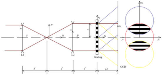
Figure 2.
Illustration of grating diffractive wavefront.
When the wafer under investigation is positioned at the co-focal plane lenses, the distribution of diffractive light intensity in the CCD sensor can be calculated as:
In this equation, d is the period of the Ronchi grating, E0 is the plural amplitude of the plane wavefront and c0/c1 is the diffractive factor of the grating. The distribution of plural amplitude, imaged by the CCD sensor, can be calculated as:
In Equation (2), r is the semi-diameter of diaphragm and Lc is the distance between the grating and the CCD sensor when the wafer is placed at a defocus position in relation to the projection lens, as shown in Figure 3.
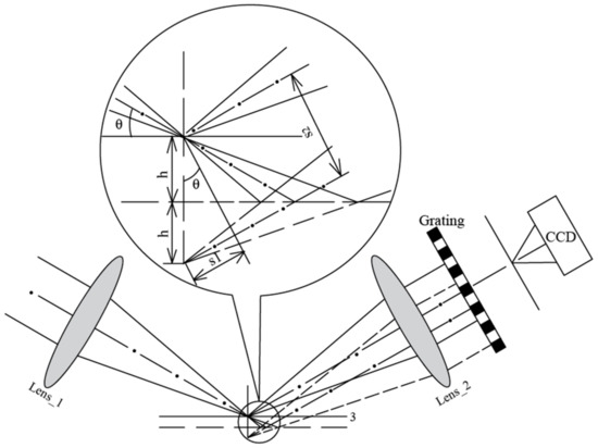
Figure 3.
Illustration of defocus measurement system.
Based on the triangle principle, the defocus of wafer can be calculated in measuring system coordinates:
In this equation, s1 and s2 are axis defocus and vertical axis defocus, respectively. Defocus s1 transforms the plane wavefront into a spherical wavefront in the 4f optical system and defocus s2 engenders a phase shift in the measurement system, as shown in Figure 4.
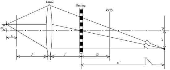
Figure 4.
Element location of focus measurement system.
To simplify the analysis, the spherical wavefront is approximated as plane wavefront ( << f). We calculated the intensity of the shearing interference area between the 0-order and ±1-order wavefronts of the grating diffractive:
The distribution of plural amplitude, imaged by the CCD sensor, can be calculated as:
By contrasting Equations (2) and (5), we note that the defocus of the wafer is calculated in this system by measuring the phase shift of the interference pattern between the 0-order and ±1-order diffractive wavefronts, showed in Figure 5.
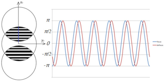
Figure 5.
Simulation of phase shift at focus and defocus position.
By contrasting the phase shift δ between the focus and defocus positions, the defocus of wafer h can be calculated:
As the parameters of the measuring system (focal length of lens f, distance between the grating and CCD sensor Lc, and the period of grating d) are fixed, the defocus of the wafer is measured by the phase extraction between the focus and defocus positions.
3. Experiment
An experiment is proceeded to verify the feasibility and calculate the measurement precision of this technology, which is conducted by the measurement system shown in Figure 6.
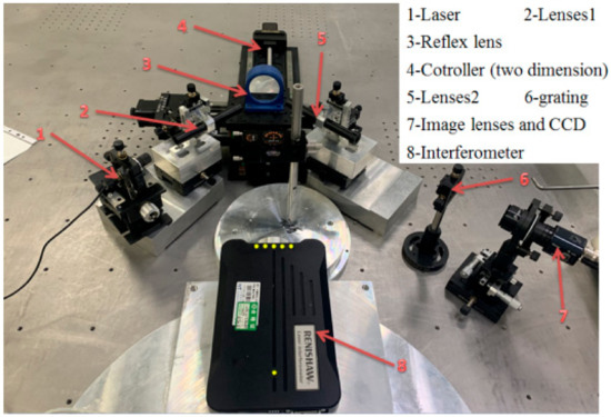
Figure 6.
Measurement system for wafer focusing technique (WFT).
When analyzed by Equation (6), the defocus of wafer can be calculated as (light way θ is 30°):
The measuring uncertainty can be calculated by:
In this equation, the measuring uncertainty is impacted by the phase extraction precision and the parameters of the measuring system (focal length of lens f, distance between the grating and CCD sensor Lc, and the period of grating d). The measurement parameter and uncertainty factor in this system are analyzed in Table 1.

Table 1.
Measurement uncertainty in the system.
The main measuring uncertainty is impacted by phase extraction precision. Instead of the wafer, a reflex lens is applied and controlled by an electronic driver and an interferometer is also applied for reference. As the Reflex lenses are driven, they form a 1000-nm defocus to focus position; the interferometry pattern detected by CCD is shown in Figure 7.
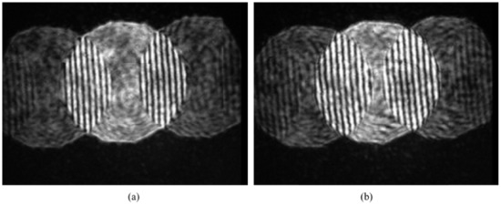
Figure 7.
Distribution of interferometry pattern detected by CCD sensor: (a) wafer at focus position; (b) wafer at defocus position.
To indicate the precision of this technique, the reflex lens, instead of the wafer, is driven by a piezo driver 1 μm from the focus to defocus position detected by the interferometer. A method based on the spatial domain phase shift technique is applied for the phase parsing of the shearing interferometry fringe.
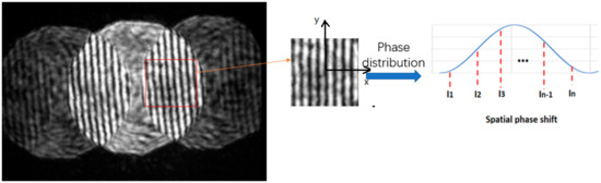
Figure 8.
Phase parsing by spatial domain phase shift technique.
We chose ten optional pixels to calculate the phase difference in the interferometry fringe between the focus and defocus positions of the wafer.
Tens of measurement results are calculated by a single shot of CCD; this method ensures measurement precision and efficiency. The measurement result is shown in Table 2.
Table 2.
Measurement result contrasted with interferometer.
After analyzing and contrasting these measurement errors using the interferometer, the final measurement precision precedes 30 nm.
4. Conclusions
On the whole, a novel WFT based on grating shearing interferometry and the spatial domain phase shift technique is introduced in detail and the measurement system is simply composed of a diffractive grating. By calibration, using an interferometer, an experiment is proposed to verify the measurement feasibility, which indicates the outstanding advantages of this WFT, including its simple setup and high measurement accuracy (30 nm).
Author Contributions
Methodology and Formal Analysis, J.W.; Investigation, S.H.; Date Curation, X.Z. All authors have read and agreed to the published version of the manuscript.
Funding
This research received no external funding.
Conflicts of Interest
The authors declare no conflict of interest.
References
- Singer, J.P.; Lee, J.-H.; Kooi, S.E.; Thomas, E.L. Rapid fabrication of 3D terahertz split ring resonator arrays by novel single-shot direct write focused proximity field nanopatterning. Opt. Express 2012, 20, 11097–11108. [Google Scholar] [CrossRef] [PubMed][Green Version]
- Chen, X.; Yao, H.; Chen, X. Classical simulation of atomic beam focusing and deposition for atom lithography. Chin. Opt. Lett. 2004, 2, 187–189. [Google Scholar]
- Keskinbora, K.; Grévent, C.; Bechtel, M.; Weigand, M.; Goering, E.; Nadzeyka, A.; Peto, L.; Rehbein, S.; Schneider, G.; Follath, R.; et al. Ion beam lithography for Fresnel zone plates in X-ray microscopy. Opt. Express 2013, 21, 11747–11756. [Google Scholar] [CrossRef] [PubMed]
- Tawarayama, K.; Aoyama, H.; Magoshi, S.; Tanaka, Y.; Shirai, S.; Tanaka, H. Recent progress of EUV full-field exposure tool in Selete. In Proceedings of the SPIE Advanced Lithography, San Jose, CA, USA, 17 March 2009; Volume 7271, p. 727118. [Google Scholar]
- Huang, T.; Liu, S.; Yi, P.; Shi, T. Focusing and leveling system for optical lithography using linear CCD. In Proceedings of the 2008 International Conference of Optical Instrument and Technology, Beijing, China, December 2008; Volume 7160, p. 71602X. [Google Scholar] [CrossRef]
- Kim, D.; Jang, W.-I.; Choi, B.-Y.; Lee, Y.I.; Lee, J.-H.; Yoo, H.J.; Kang, S.W.; Kwon, J.H. Focusing and leveling system using position-sensitive detectors for the wafer steppers. In Proceedings of the SPIE’s 1994 Symposium on Microlithography, San Jose, CA, USA, 17 May 1994; Volume 2197, p. 997. [Google Scholar]
- Rhee, H.-G.; Lee, Y.-W. Enhancement of height resolution in direct laser lithography. Opt. Express 2012, 20, 291–298. [Google Scholar] [CrossRef] [PubMed]
- Williams, W.; Saffman, M. Two-dimensional atomic lithography by submicrometer focusing of atomic beams. J. Opt. Soc. Am. B 2006, 23, 1161–1169. [Google Scholar] [CrossRef]
- Unno, Y. Modeling of a slit-scan-type aerial image measurement sensor used for optical lithography. Appl. Opt. 2011, 50, 271–281. [Google Scholar] [CrossRef] [PubMed]
- Hori, Y.; Sogawa, F.; Asakure, H.; Kato, M.; Serizawa, H. Fabrication of a focusing grating mirror by electron beam lithography. Appl. Opt. 1990, 29, 2522–2526. [Google Scholar] [CrossRef] [PubMed]
- Yan, W.; Yang, Y.; Chen, W.; Hu, S.; Zhou, S. Moiré-based focusing and leveling scheme for optical projection lithography. Appl. Opt. 2010, 49, 5959–5963. [Google Scholar] [CrossRef]
- Zhu, J.; Hu, S.; Yu, J.; Tang, Y.; Xu, F.; He, Y.; Zhou, S.; Li, L. Influence of tilt moiré fringe on alignment accuracy in proximity lithography. Opt. Laser. Eng. 2013, 51, 371–381. [Google Scholar]
- Watanabe, M.; Oshida, Y.; Nakayama, Y.; Yoshida, M.; Funatsu, R.; Fujii, A.; Ninomiya, T. Focusing and leveling based on wafer surface profile detection with interferometry for optical lithography. In Proceedings of the SPIE’s 1994 Symposium on Microlithography, San Jose, CA, USA, 17 May 1994; Volume 2197, p. 980. [Google Scholar]
- Dong, B.; Zhang, G.; Yang, G.; Gu, B.; Zheng, S.; Li, D.; Chen, Y.; Cui, X.; Chen, M.; Liu, H. Design and fabrication of a diffractive phase element for wavelength demultiplexing and spatial focusing simultaneously. Appl. Opt. 1996, 35, 6859–6864. [Google Scholar] [PubMed]
- Malacara, D. Optical Shop Testing; John Wiley & Sons, Inc.: Hoboken, NJ, USA, 2007; Chapter 8. [Google Scholar]
- Wu, J.; Chen, J.; Xu, A.; Gao, X.; Zhuang, S. Focal length measurement based on Hartmann-Shack principle. Opt. Int. J. Light Electron 2011. [Google Scholar] [CrossRef]
- Memmolo, P.; Finizio, A.; Paturzo, M.; Miccio, L.; Ferraro, P. Twin-beams digital holography for 3D tracking and quantitative phase-contrast microscopy in microfluidics. Opt. Express 2011, 25, 25833–25842. [Google Scholar]


Publisher’s Note: MDPI stays neutral with regard to jurisdictional claims in published maps and institutional affiliations. |
© 2020 by the authors. Licensee MDPI, Basel, Switzerland. This article is an open access article distributed under the terms and conditions of the Creative Commons Attribution (CC BY) license (http://creativecommons.org/licenses/by/4.0/).