Article

Investigation on the Hump Behavior of Gate-Normal Nanowire Tunnel Field-Effect Transistors (NWTFETs)

Department of Electronic Engineering, Sogang University, Seoul 04107, Korea
*
Author to whom correspondence should be addressed.
Appl. Sci. 2020, 10(24), 8880; https://doi.org/10.3390/app10248880
Submission received: 27 October 2020 / Revised: 6 December 2020 / Accepted: 10 December 2020 / Published: 11 December 2020
(This article belongs to the Special Issue Device Modeling for TCAD and Circuit Simulation)

Abstract

:
The hump behavior of gate-normal nanowire tunnel field-effect transistors (NWTFETs) is investigated by using a three-dimensional technology computer-aided design (TCAD) simulation. The simulation results show that the hump behavior degrades the subthreshold swing (SS) and on-current (Ion) because the corners and sides of nanowires (NWs) have different surface potentials. The hump behavior can be successfully suppressed by increasing the radius of curvature (R) of NWs and reducing gate insulator thickness (Tins).

1. Introduction

The aggressive downscaling of metal oxide semiconductor field-effect transistors (MOSFETs) has raised some problems regarding the off-current (Ioff) and supply voltage [1]. A tunnel field-effect transistor (TFET) has been considered as one of the most promising candidates for extremely low-power applications thanks to its low Ioff and abrupt on–off switching [2,3]. However, TFETs suffer from low on-current (Ion) [4]. For higher Ion, several strategies have been proposed: the introduction of low bandgap materials [5], and hetero-gate-dielectric (HG) [6] and hetero-material-gate (HMG) structures [7]. Additionally, gate-normal TFETs were proposed to boost Ion by increasing the tunneling cross-sectional area [8,9,10,11]. The band-to-band tunneling (BTBT) generation of gate-normal TFETs occurs perpendicular to the channel in the gate–source overlap region. Thus, the gate-normal tunneling area can be enlarged by increasing the gate–source overlap length (Lov) to increase Ion.
Recently, silicon nanowire (SiNW) TFETs have been developed for superior subthreshold swing (SS), Ioff, and short-channel-effect immunity [12,13]. The fabrication of SiNW TFETs using a top-down process has great advantages in terms of being a reproducible process, having compatibility with CMOS and having good control over the dimensions, while a bottom-up process has been seriously limited due to a difficulty in the fabrication process [14,15,16]. In this manuscript, as shown in Figure 1, gate-normal NWTFETs are discussed, which combine the advantages of gate-normal TFETs and NWFETs. One of the most serious problems of gate-normal NWTFETs is the hump behavior stemming from the three-dimensional corner effect: the surface potentials are different between the corner and side of an NW. This means that different BTBT turn-on voltages exist in an NW, which induces the hump behavior of degrading SS and Ion [17]. Thus, it is necessary to suppress the corner effect of gate-normal NWTFETs. There are several studies on the hump behavior of TFETs and various methods of mitigating hump behavior [18,19,20,21]. However, this study discusses the hump behavior originated from the geometrical effect of the three-dimensional NW structure. Even if many studies have been performed regarding the corner effect of NWMOSFETs [22,23,24,25], that of gate-normal NWTFETs has rarely been discussed.
In this manuscript, the hump behavior of gate-normal NWTFETs is investigated and its solution is proposed by three-dimensional (3D) technology computer-aided design (TCAD) simulation.

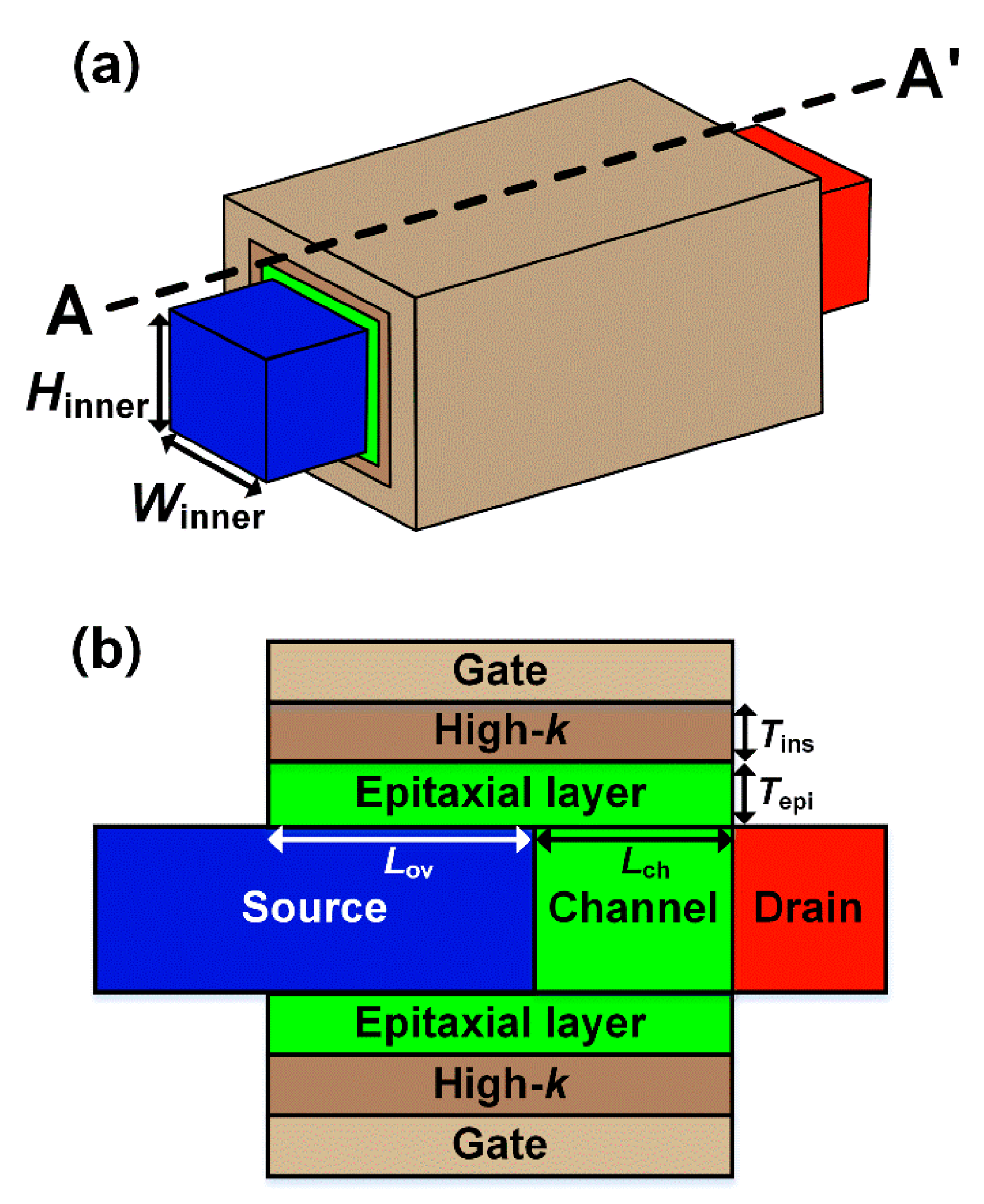
2. Device Structure and Simulation Methodology

Figure 1 shows the bird’s eye and cross-sectional views of gate-normal NWTFETs. It features a gate–source overlapped thin intrinsic epitaxial layer to fix the tunnel width. The device parameters are summarized in Table 1. The channel length (Lch) is 20 nm. The gate–source overlap length (Lov) is 40 nm. Both the inner width (Winner) and inner height (Hin ner) are 20 nm, respectively. The gate insulator thickness (Tins) is 2 nm. The epi-layer thickness (Tepi) is 2 nm. The source (NS) and drain doping concentrations (ND) are 1020 cm-3, respectively.
3D TCAD device simulation has been performed by using a commercial simulator [26]. For the accurate calculation of the BTBT generation rate, a dynamic nonlocal BTBT model is used after calibration [27]. Additionally, the Shockley–Read–Hall recombination, Philips unified mobility model and Fermi distribution are used in our simulation. On the contrary, quantization effects and the gate leakage current have not been considered. The threshold voltage (VT) is defined as the gate voltage (VG) when the drain current (ID) is equal to 0.1 nA/μm, while the turn-on voltage (Vturn-on) is defined as VG when ID is equal to 0.01 fA/μm. The Ion and Ioff are defined as ID when the overdrive voltages (VGVturn-on) are 0.5 V and −0.2 V, respectively. The average SS (SSavg) is calculated from VG = Vturn-on to VG = Vturn-on + 0.5 V. Drain-induced barrier thinning (DIBT) is calculated as the VT difference between VD = 0.05 V and 0.5 V.

3. Simulation Results and Discussion

3.1. Analysis of Hump Behavior of Gate-Normal NWTFETs

Figure 2 shows the simulated transfer curves of the gate-normal NWTFETs, which show clear hump behavior degrading SS and Ion. Two noteworthy phenomena are observed. First, hump behavior occurs and the SS is abruptly changed around VG = 0.7 V. In order to analyze the hump behavior, the electron BTBT generation rates in the gate–source overlap region are simulated at around VG = 0.7 V at VD = 0.5 V. As shown in Figure 3, gate-normal BTBT occurs at the corners earlier than at the sides, which is called the corner effect. To be specific, the area wherein BTBT occurs is extended from the corner to the side as VG increases. In addition, the electron BTBT generation rate is not constant through the NW, and is stronger at the corner. This means that different BTBT turn-on voltages exist in an NW, which induce the hump behavior. Second, as shown in Figure 2, the hump becomes more severe as VD decreases. At low VD, it is vulnerable to the hump because the influence of the gate increases as the VD decreases, while the hump is more affected by the structure of the gate.
The definition of the corner and side of an NW is shown in Figure 4. Because the tunneling width is determined by the epi-layer thickness (Tepi), gate-normal tunneling occurs mainly in the epi-layer [28]. Thus, by integrating electron BTBT generation rates over the cross-section of an NW, electron BTBT generation rates per channel length are calculated. In order to evaluate the influence of the corners on ID, the electron BTBT generation rates at the corners and sides are compared with each other. Figure 5 shows that gate-normal tunneling occurs first in the corner region and then in the side region of an NW. The corner effect is dominant at a low VG while it becomes less strong as VG increases. Thus, it degrades the on–off transition abruptness of the total electron BTBT generation rates. Figure 6a shows the 2D contour of electrostatic potential. As shown in Figure 6b,c, the surface potential is higher at the corner than at the side in the entire range of VG. This is because the charge at the corner is shared by the surrounding gate. The charge sharing effect at the corner contributes to the higher surface potential compared with the side one [29,30]. The difference in surface potentials in an NW affects the energy band diagrams of gate-normal NWTFETs. Figure 7 shows the energy band diagrams extracted, at the corner and side, from the middle of the gate–source overlap region, respectively. Gate-normal tunneling, which is a main current mechanism of the gate-normal NWTFETs, occurs vertically in the gate–source overlap region, whereas the current is conducted laterally along the gate-controlled surface channel [10]. Then, in order to induce gate-normal tunneling, the band alignment in the direction perpendicular to the channel in the gate–source overlap region should be required [28]. When the VG is 0.6 V, the conduction energy band edge (EC) of the epi-layer is aligned with the valence energy band edge (EV) of the source region at the corner, while the EC of the epi-layer is not aligned with the EV of the source region at the side. This is because the higher surface potential of the corner leads the energy band of the surface to shift down, which causes the gate-normal tunneling to turn on early. Thus, the corner and side of an NW have different BTBT turn-on voltages, which induce the hump behavior.

3.2. Hump Suppression by Rounding NW Corners and Reducing Gate Insulator Thickness

In order to improve the SS and Ion of the gate-normal NWTFETs, the hump behavior must be suppressed. In this paragraph the radius of curvature (R) of an NW and Tins are optimized for the suppression of the hump behavior. The normalized R (Rnorm) is defined as 2R/Winner. The three Rnorm values are discussed as shown in Figure 8: 0, 0.4, and 1. Figure 9 shows the simulated transfer curves of the gate-normal NWTFETs with various Rnorms ranging from 0 to 1. As the Rnorm increases, the hump behavior becomes weaker because the surface potential difference between the corner and side becomes smaller, as shown in Figure 10. The surface potential difference in an NW becomes 0 as Rnorm becomes 1. In addition, as the corner behavior is alleviated, the short channel behavior is suppressed down [22,23]. Thus, it is observed that the Vturn-on increases, the SSavg improves, the Ion/Ioff ratio increases, and the DIBT decreases, as shown in Figure 11. In the case of a cylindrical NW whose Rnorm is 1, the gate-normal BTBT evenly occurs on the entire surface. The gate-normal NWTFET whose Rnorm is 1 shows a twofold higher Ion and a 5.4-fold higher Ion/Ioff than that whose Rnorm is 0.
Another way to suppress the hump behavior is to reduce the Tins. Figure 12 shows the simulated transfer curves with various Tinss. As Tins decreases, that hump is suppressed and the SS is improved because the gate’s controllability over the channel becomes better. The surface potential on the gate–source overlap region increases as the Tins decreases. However, as shown in Figure 13a, the potential at the side becomes higher than that at the corner as the Tins decreases. It should be noted that the potential at the corner is less sensitive to Tins than that at the side because the corners of an NW are surrounded by the gate [17]. Thus, as shown in Figure 13b, the surface potential difference between the corner and side decreases as the Tins decreases. In other words, the difference in BTBT turn-on voltages in an NW is reduced, which means less hump behavior.

4. Conclusions

The hump behavior of gate-normal NWTFETs is analyzed by using 3D TCAD simulation. It is discussed that the hump originates from the corner effect induced by the surrounding gate. BTBT occurs at the corner earlier than at the side due to the higher surface potential at the corner. By increasing Rnorm and decreasing Tins, the hump behavior can be suppressed. Cylindrical gate-normal NWTFETs with low Tins are recommended for extremely low-power applications.

Author Contributions

Writing—original draft and data curation, M.W.K.; formal analysis, M.W.K.; writing—review and editing, W.Y.C.; validation W.Y.C.; supervision W.Y.C. All authors have read and agreed to the published version of the manuscript.

Funding

This work was supported in part by the NRF of Korea funded by the MSIT under Grant NRF-2019M3F3A1A02072089 (Intelligent Semiconductor Technology Development Program), NRF-2018R1A2A2A05019651 (Mid-Career Researcher Program), NRF-2016M3A7B4909668 (Nano-Material Technology Development Program), in part by the IITP funded by the MSIT under Grant IITP-2020-2018-0-01421 (Information Technology Research Center Program), and in part by the MOTIE/KSRC under Grant 10080575 (Technology Innovation Program).

Conflicts of Interest

The authors declare no conflict of interest.

References

  1. Bangsaruntip, S.; Cohen, G.M.; Majunmdar, A.; Sleight, J.W. Universality of short-channel effects in undoped-body silicon nanowire MOSFETs. IEEE Electron Device Lett. 2010, 31, 903–905. [Google Scholar] [CrossRef]
  2. Ionescu, A.M.; Riel, H. Tunnel field-effect transistors as energy-efficient electronic switches. Nature 2011, 479, 329–337. [Google Scholar] [CrossRef] [PubMed]
  3. Seabaugh, A.C.; Zhang, Q. Low-Voltage Tunnel Transistors for Beyond CMOS Logic. Proc. IEEE 2010, 98, 2095–2110. [Google Scholar] [CrossRef]
  4. Choi, W.Y.; Park, B.G.; Lee, J.D.; Liu, T.J.K. Tunneling Field-Effect Transistors (TFETs) with Subthreshold Swing (SS) Less Than 60 mV/dec. IEEE Electron Device Lett. 2007, 28, 743–745. [Google Scholar] [CrossRef]
  5. Knoch, J.; Appenzeller, J. Modeling of high-performance p-type Ⅲ-Ⅴ heterojunction tunnel FETs. IEEE Electron Dev. Lett. 2010, 31, 305–307. [Google Scholar] [CrossRef]
  6. Choi, W.Y.; Lee, W. Hetero-Gate-Dielectric Tunneling Field-Effect Transistors. IEEE Electron Dev. Lett. 2010, 57, 2317–2319. [Google Scholar] [CrossRef]
  7. Beneventi, G.B.; Gnani, E.; Gnudi, A.; Reggiani, S.; Baccarani, G. Dual-metal-gate InAs tunnel FET with enhanced turn-on steepness and high ON-current. IEEE Electron Dev. Lett. 2014, 61, 776–784. [Google Scholar] [CrossRef]
  8. Hsu, W.; Mantey, J.; Register, L.F.; Banerjee, S.K. Strained-Si/strained-Ge type-Ⅱ staggered heterojunction gate-normal-tunneling field-effect transistor. Appl. Phys. Lett. 2013, 103, 093501. [Google Scholar] [CrossRef]
  9. Hsu, W.; Mantey, J.; Register, L.F.; Banerjee, S.K. On the Electrostatic Control of Gate-Normal Tunneling Field-Effect Transistors. IEEE Electron Dev. Lett. 2015, 62, 2292–2299. [Google Scholar] [CrossRef]
  10. Shih, C.H.; Chie, N.D. Design and modeling of line-tunneling field-effect transistors using low-bandgap semiconductors. IEEE Electron Dev. Lett. 2014, 61, 1904–1913. [Google Scholar] [CrossRef]
  11. Wang, P.Y.; Tsui, B.Y. Epitaxial tunnel layer structure for P-channel tunnel FET improvement. IEEE Electron Dev. Lett. 2013, 60, 4098–4104. [Google Scholar] [CrossRef]
  12. Gandhi, R.; Chen, Z.; Singh, N.; Banerjee, K.; Lee, S. Vertical Si-nanowire n-type tunneling FETs with low subthreshold swing (≤ 50mV/decade) at room temperature. IEEE Electron Dev. Lett. 2011, 32, 437–439. [Google Scholar] [CrossRef]
  13. Smith, J.T.; Sandow, C.; Das, S.; Minamisawa, R.A.; Mantl, S.; Appenzeller, J. Silicon nanowire tunneling field-effect transistor arrays: Improving subthreshold performance using excimer laser annealing. IEEE Electron Dev. Lett. 2011, 58, 1822–1829. [Google Scholar] [CrossRef]
  14. Tran, D.P.; Pham, T.T.T.; Wolfrum, B.; Offenhausser, A.; Thierry, B. Cmos-compatible silicon nanowire field-effect transistor biosensor: Technology development toward commercialization. Materials 2018, 11, 785. [Google Scholar] [CrossRef] [PubMed] [Green Version]
  15. Lee, M.; Koo, J.; Chung, E.A.; Jeong, D.Y.; Koo, Y.S.; Kim, S. Silicon nanowire-based tunneling field-effect transistors on flexible plastic substrates. Nanotechnology 2009, 20, 455201–455206. [Google Scholar] [CrossRef] [PubMed]
  16. Lee, K.N.; Jung, S.W.; Kim, W.H.; Lee, M.H.; Shin, K.S.; Seong, W.K. Well controlled assembly of silicon nanowires by nanowire transfer method. Nanotechnology 2007, 18, 445302. [Google Scholar] [CrossRef]
  17. Lee, W.; Choi, W.Y. Quantitative analysis of hump effects of Gate-All-Around Metal-Oxide-Semiconductor Field-Effect Transistors. JJAP 2010, 49, 04DC11. [Google Scholar] [CrossRef]
  18. Kim, H.W.; Sun, M.C.; Kim, S.W.; Park, B.G. Hump Phenomenon in Transfer Characteristics of Double-Gated Thin-Body Tunneling Field-Effect Transistor (TFET) with Gate/Source Overlap. In Proceedings of the IEEE 5th International Nanoelectronics Conference (INEC), Singapore, 2–4 January 2013; pp. 364–366. [Google Scholar]
  19. Kim, S.W.; Choi, W.Y. Hump effects of germanium/silicon heterojunction tunnel field-effect transistors. IEEE Electron Dev. Lett. 2016, 63, 2583–2588. [Google Scholar] [CrossRef]
  20. Lee, S.H.; Park, J.U.; Kim, G.; Jee, D.W.; Kim, J.H.; Kim, S.W. Rigorous Study on Hump Phenomena in Surrounding Channel Nanowire (SCNW) Tunnel Field-Effect Transistor (TFET). Appl. Sci. 2020, 10, 3596. [Google Scholar] [CrossRef]
  21. Kwon, Y.S.; Lee, S.H.; Kim, Y.; Kim, G.; Kim, J.H.; Kim, S.W. Surrounding Channel Nanowire Tunnel Field-Effect Transistor with Dual Gate to Reduce a Hump Phenomenon. J. Nanosci. 2020, 20, 4182–4187. [Google Scholar]
  22. Lee, C.W.; Yun, S.R.N.; Yu, C.G.; Park, J.T.; Colinge, J.P. Device design guidelines for nano-scale MuGFETs. Solid State Electron. 2007, 51, 505–510. [Google Scholar] [CrossRef]
  23. Song, J.Y.; Choi, W.Y.; Park, J.H.; Lee, J.D.; Park, B.G. Design optimization of gate-all-around (GAA) MOSFETs. IEEE T Nanotechnol. 2006, 5, 186–191. [Google Scholar] [CrossRef]
  24. Ruiz, F.J.G.; Godoy, A.; Gamiz, F.; Sampedro, C.; Donetti, L. A comprehensive study of the corner effects in pi-gate SOI MOSFETs including quantum effects. IEEE Electron Dev. Lett. 2007, 54, 3369–3377. [Google Scholar] [CrossRef]
  25. Fossum, J.G.; Yang, J.W.; Trivedi, V.P. Suppression of corner effects in triple-gate MOSFETs. IEEE Electron Device Lett. 2003, 24, 745–747. [Google Scholar] [CrossRef]
  26. Synopsys. User Manual; Version L-2016.03, Synopsys TCAD Sentaurus; Synopsys: San Jose, CA, USA, 2016.
  27. Kao, K.H.; Verhulst, A.S.; Vandenberghe, W.G.; Sorée, B.; Groeseneken, G.; De Meyer, K. Direct and indirect band-to-band tunneling in germanium-based TFETs. IEEE Electron Dev. Lett. 2012, 59, 292–301. [Google Scholar] [CrossRef]
  28. Kim, S.W.; Choi, W.Y.; Sun, M.C.; Kim, H.W.; Park, B.G. Design guideline of Si-based L-Shaped Tunneling Field-Effect Transistors. JJAP 2012, 51, 06FE03-1–06FE03–5. [Google Scholar]
  29. Liu, L.; Liang, R.; Zhao, L.; Wang, J.; Xu, J. Influence of corner effect on performance of three-dimensional tunnel field-effect transistor. JJAP 2014, 53, 064304. [Google Scholar] [CrossRef]
  30. Tseng, P.H.; Hwu, J.G. Convex corner induced capacitance-voltage response from depletion to deep depletion in non-planar substrate metal-oxide-semiconductor capacitors with ultra thin oxide. Thin Solid Films. 2014, 556, 317–321. [Google Scholar] [CrossRef]
Figure 1. (a) Bird’s eye and (b) cross-sectional views of simulated gate-normal nanowire tunnel field-effect transistors (NWTFETs) with the normalized radius of curvature (Rnorm) of 0.
Applsci 10 08880 g001
Figure 2. Transfer curves of the gate-normal NWTFETs for VD values of 0.5 V and 0.05 V. It is shown that gate-normal NWTFETs suffer from hump behavior, which degrades SS and Ion.
Applsci 10 08880 g002
Figure 3. 3D and 2D contour plots of electron band-to-band tunneling (BTBT) generation rates of gate-normal NWTFETs at VG = 0.6V, 0.7V, and 0.8V at VD = 0.5V.
Applsci 10 08880 g003
Figure 4. Definition of corner and side of a nanowire (NW).
Applsci 10 08880 g004
Figure 5. Electron BTBT generation rates per channel length extracted in the corner, side and total region as a function of VG.
Applsci 10 08880 g005
Figure 6. (a) 2D contour of electrostatic potential distribution at VG = 1.5 V, (b) electrostatic potential of cut line as VG increases (0.5 V–1.5 V), (c) surface potential at the corner and side.
Applsci 10 08880 g006
Figure 7. Energy band diagrams of the gate-normal NWTFETs extracted at the (a) corner and (b) side.
Applsci 10 08880 g007
Figure 8. Cross-section of NWs with different Rs.
Applsci 10 08880 g008
Figure 9. Transfer characteristics of gate-normal NWTFETs with the variation in the normalized radius of curvature of the corners (Rnorm) from 0 to 1. It is shown that the hump is suppressed with the increasing of Rnorm.
Applsci 10 08880 g009
Figure 10. Surface potential difference between the corner and side with the variation in Rnorm.
Applsci 10 08880 g010
Figure 11. (a) SSavg and Vturn-on, (b) DIBT, (c) Ion and Ioff and (d) Ion/Ioff ratio as a function of Rnorm.
Applsci 10 08880 g011
Figure 12. Transfer characteristics of NW gate-normal TFETs with the variation in thickness of gate insulator (Tins).
Applsci 10 08880 g012
Figure 13. (a) Electrostatic potential with the variation in Tins at VG = 1 V; (b) Surface potential difference between the corner and side with the variation in Tins.
Applsci 10 08880 g013
Table 1. Device parameters for simulation.
ParametersValues
Lch20 nm
Lov40 nm
Winner, Hinner20 nm
Tins2 nm
Tepi2 nm
NS1 × 1020 cm−3 (p-type)
ND1 × 1020 cm−3 (n-type)
Nch, NepiIntrinsic
Publisher’s Note: MDPI stays neutral with regard to jurisdictional claims in published maps and institutional affiliations.

