Article

Influence of the Secondary Ion Beam Source on the Laser Damage Mechanism and Stress Evolution of IBS Hafnia Layers

1
RhySearch, The Rhine Valley Research and Innovation Center, Werdenbergstrasse 4, 9471 Buchs, Switzerland
2
Laboratoire Temps-Fréquence, Institut de Physique, Université de Neuchâtel, 2000 Neuchâtel, Switzerland
*
Author to whom correspondence should be addressed.
Appl. Sci. 2021, 11(1), 189; https://doi.org/10.3390/app11010189
Submission received: 11 December 2020 / Revised: 23 December 2020 / Accepted: 24 December 2020 / Published: 28 December 2020
(This article belongs to the Special Issue Laser Material Manufacturing)

Abstract

:
Ion beam sputtered hafnia is a preferred high index coating material for laser applications. It exhibits a mostly amorphous structure and an adequate laser-induced damage (LIDT) threshold. In this work, we investigated the influence of an assisting ion source on the film stress as well as the LIDT of the sputtered hafnia layers. The stress increases with an increasing ion energy of the assisting ion beam. We identified a maximum compressive stress of 3–3.5 GPa before the film cracks, blisters, and delaminates. Different states of stress lead to different laser-induced damage thresholds and damage morphologies.

1. Introduction

Elements for laser optics are typically coated with multilayer interference coatings for antireflection, high reflectance, or wavelength, as well as polarization separation [1,2]. In most cases, interference coatings consist of two materials with a high and a low refractive index, respectively. In the case of high-end laser applications, a widely used high index material is hafnia—in this work, HfO2 is deposited by means of ion beam sputtering (IBS). It exhibits low absorption in the entire spectral range, from the UV to NIR [3,4], and a high laser damage threshold (LIDT) [4,5]. It is also interesting for electronic applications as a gate oxide to replace SiO2 due to its higher dielectric constant [6,7].
During layer deposition, an assisting ion beam is often directed to the substrate to tune the quality of the deposited layers. If the primary deposition method is evaporation, the technique is called ion beam assisted deposition (IAD), while in the case of IBS it is called dual ion beam sputtering (DIBS). The assisting source has several advantages. An ion beam can be applied for surface pre-cleaning; it can also be used to provide excited oxygen for better film oxidation and additional high energetic excited oxygen atoms for densifying the films [8].
For several coating applications, thin-film stress plays an important role. The stress effects from assisted deposition has been researched since the 1990s [9,10]. Stress is especially important in the case of thick single- as well as multi-layer stacks (i.e., high reflectance coatings) [4,11]. Stress can lead to (partial) crystallization [12,13], with suboptimal optical performance or, in the catastrophic case, delamination of the film [14]. The kinetic energy of the impinging atoms influences the thin-film stress. E-beam-deposited thin films exhibit low stress due to the low kinetic energy of the film-building atoms. With increasing energy, the film stress becomes compressive (e.g., magnetron sputtering). This compressive stress increases further with increasing kinetic energy (e.g., IBS, high-power impulse magnetron sputtering (HiPIMS)). In the case of IBS, there are several studies on other materials where the properties are improved by using the second ion beam source. In the case of Ta2O5, stress is reduced and the visible and NIR transmittance is increased at an intermediate level (350–450 V) of the assisting ion beam voltage [15].
In this work, we investigated the influence of the assisting ion beam source on the properties of HfO2 single layers deposited by IBS.

2. Materials and Methods

2.1. HfO2 Thin Film Deposition

We deposited single HfO2 layers with thicknesses of 100 and 480 nm, respectively, by means of reactive ion beam sputtering using a metallic Hf-target (Plasmaterials with 3N purity excluding the Zr impurities). We used single-crystalline Si substrates (001 orientation; P-doped; 10 mm × 10 mm × 525 μm) from CrysTec GmbH for stress as well as ellipsometry measurements. For LIDT measurements, we used fused silica substrates (3 Å rms roughness, 1” diameter, 2 mm thickness) provided by WZWoptic AG. The fused silica substrates were cleaned before coating on a wet bench in a cleanroom environment (for more detail see [14]) to reduce the influence of process-related contamination on the LIDT measurements. Furthermore, all coating activities were performed under ISO 5–7 cleanroom environment.
The ion beam sputtering was performed using a Veeco Spector 1.5 DIBS system equipped with two ion beam sources: the primary 16 cm ion beam source for sputtering and the assisting 12 cm ion beam source. The primary source operates using Ar gas, while the assisting source uses an Ar/O2 mixture. In the current experiment, we used 3 sccm Ar and 8 sccm O2. The chamber pressure was in the range of 3.5 ± 0.5 × 10⁻⁴ torr during the target cleaning and deposition steps. The coating chamber was pre-heated to process saturation temperature of about 100 °C during thin film deposition. Since the DIBS system is not equipped with an active temperature stabilization, the temperature can increase during the operation of the assisting source.
To investigate the influence of the kinetic energy of the excited oxygen atoms, we varied the voltage and the current of the second ion beam source. In Table 1, the parameters of the sputter runs are summarized in more detail.

2.2. Film Stress Measurement

The film stress was estimated by measuring the curvature of the Si-substrates prior to and after thin film deposition using a Twyman-Green interferometer (FISBA OPTIK FS-50 μPhase® 2 HR). The film stress was then calculated using Stoney’s equation:
σ = E s 6 ( 1 υ s ) h s 2 h f ( 1 R 1 R 0 )
where Es, νs and hs are the Young’s modulus, the Poisson’s ratio and the thickness of the substrate, respectively, hf is the thickness of the film, and R0 and R are the radii of curvature before and after coating, respectively. We used a Young’s modulus of 170 GPa and a Poisson’s ratio of 0.064 according to Table VI in Ref. [16] for evaluating the results. The physical thickness of the films was determined by means of a KLA Tencor P-17 tactile profilometer and verified with the spectral ellipsometer.

2.3. Thin Film Crystal Structure

We investigated the crystallinity of the HfO2 films by X-ray diffractometry using a Panalytical X’Pert Pro-MRD diffractometer equipped with a Cu Kα source. The measurements were performed under a grazing incidence angle geometry using a 20°–80° 2θ range.

2.4. Optical Properties and Laser-Induced Damage Testing

The refractive index n and the extinction coefficient k were measured by ellipsometry using a SENresearch 4.0 SER 850 DUV from SENTECH Instruments at 5 angles of incidence from 50° to 70° in 5° steps combined with transmission data measured with an AGILENT Cary 5000 UV-VIS-NIR Spectrophotometer measured at an angle of incidence of 0°. Using SpectraRay 4 software from the ellipsometer, we applied a Tauc–Lorentz model with two oscillators and fitted it to the ellipsometric and transmission data.
The measurement of the LIDT was performed at the laser damage test bench located at the RhySearch optical coating laboratory [17,18]. Herewith the fused silica substrates coated with 480 nm HfO2 at 100 °C and different applied second ion beam parameters were laser damage-tested. The samples were laser irradiated under an angle of incidence of 5° in filtered air and at room temperature. The laser irradiation at 1064 nm was performed using a Montfort Nano diode-pumped Nd:YAG laser system. The effective pulse duration was about 10 ns and the repetition rate was 80 Hz. An S-on-1 measurement strategy was applied with S = 5000. The centered test area had a diameter of 20 mm and was divided into a hexagonal test matrix with 223 testing sites. The distance between the adjacent test point was 1.2 mm. The detection of damage events was done by a scattered light detector placed in front of the test sample. In order to verify the detected damage events, a visual inspection by means of differential interference contrast microscopy (Leica DM4000 M Led) was performed.
The fluence of the pulses went up to 400 Jcm−2, while the effective beam diameter (1/e2) of the Gaussian beam profile was about 45 μm. This small beam size is advantageous to study the properties of the pure, defect-free material, as the probability of irradiating a defect site is relatively low.

3. Results

3.1. Thin-Film Structure

Figure 1 shows typical optical microscopy pictures from the 480 nm-thick HfO2 layers deposited with different voltage and power levels of the assisting ion beam source. Without extraction of the ion beam (Uassist = 0 V), the film exhibits high-quality continuous nearly defect-free state (Figure 1a). With beam extraction (Uassist > 0 V), the films show defects and start to crack or delaminate whereas the defect density increases with increasing voltage and power (Figure 1b,c). After a certain threshold, the film shows nearly complete blistering, resulting in a total failure of the coating (Figure 1d). In this state, the thickness monitoring as well as the ex situ thickness measurement by profilometry was highly inaccurate due to the blistering.
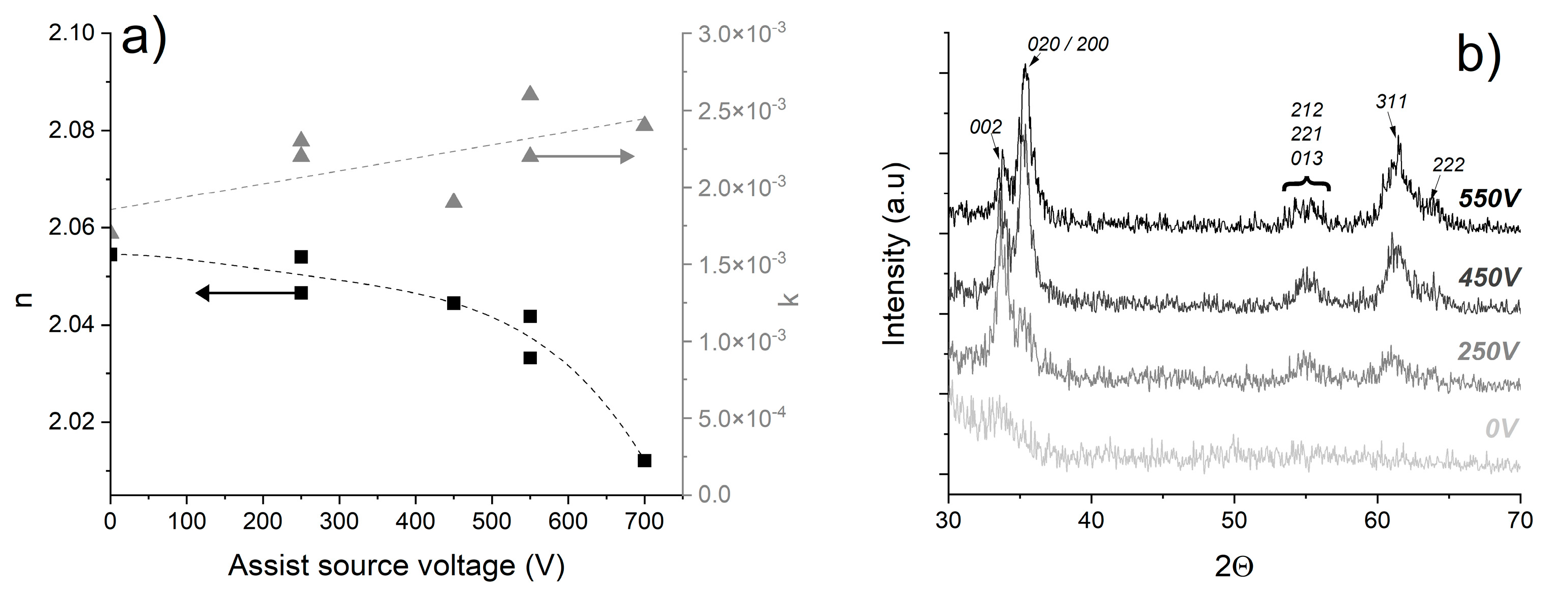
In order to estimate the refractive index and the absorbance, we performed ellipsometry measurements. Figure 2a shows the results as a function of beam voltage of the assisting ion beam source for a reference wavelength of 633 nm. The initial refractive index without extracting the assisting ion beam is about 2.05, with an extinction k of about 0.0017. With extraction above a Uassist = 250 V of the ion beam at the assisting source, a decrease in the refractive index is observed. In the case of the absorption, an increase with increasing beam voltage is observed. This is in contrast to the Ta2O5, where the best parameters are achieved at intermediate assist voltage values [15]. For the highest applied ion beam voltage Uassist, the refractive index is around 1–2% smaller and absorption is approximately 50% higher, whereas an influence due to the delamination cannot be excluded.
In Figure 2b, the grazing incidence XRD measurements of the 480 nm-thick HfO2 single layers are shown for different assisting ion beam voltages. The films prepared with IBS with the assisting source turned off appear almost X-ray-amorphous. With increasing voltage of the assisting source, the monoclinic HfO2 peaks become clearly visible.

3.2. Thin Film Stress

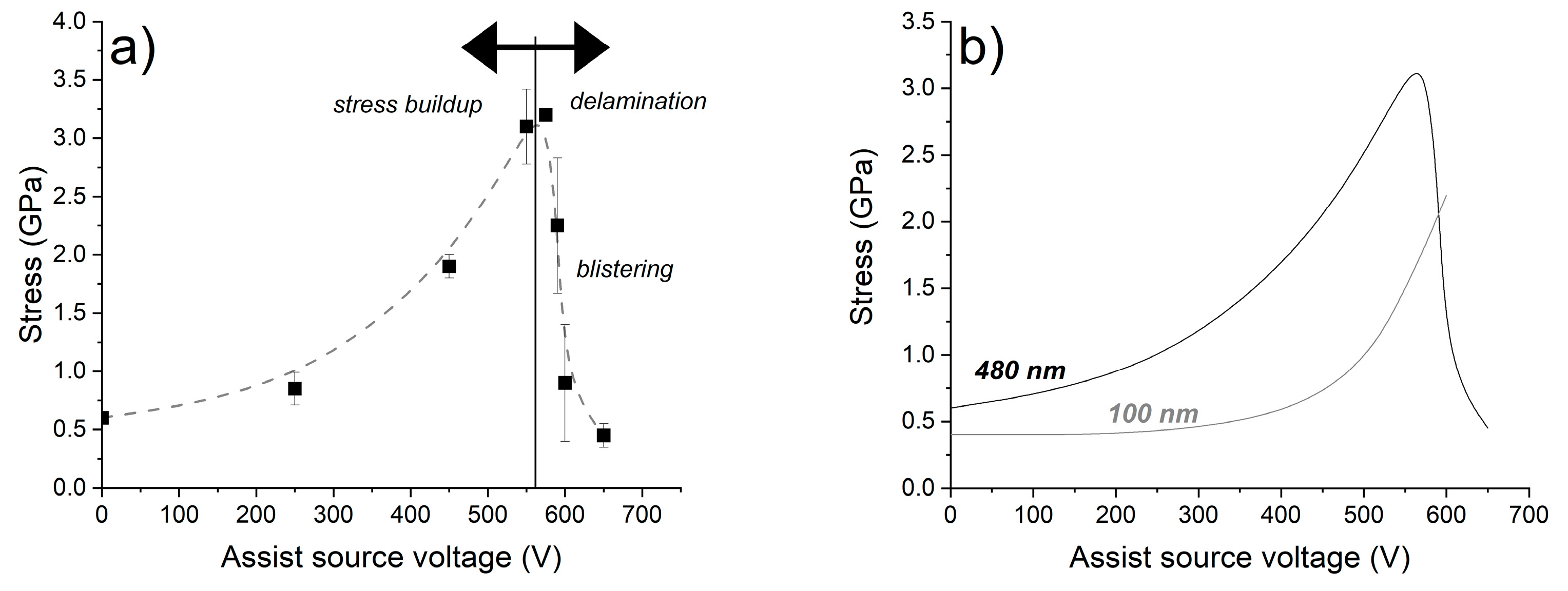
Before and after the deposition of the HfO2 single layers, the curvatures of the Si-substrates were measured. The film stress was calculated for each sample using Equation (1). Figure 3 shows the results of the stress calculation for Si-substrates coated with 480 nm HfO2 at 100 °C and various beam voltages of the assisting ion beam source. The data are approximated by a spline fit. As can be seen, the evolution of the film stress can be clearly divided into two regions: (I) stress build-up and (II) stress breakdown. In region (I), a monotone increase in the film stress is observed. For non-extraction of a beam (Uassist = 0 V), the stress starts with an initial value of about 0.6 GPa. With the extraction of the beam, the stress increases continuously with the increasing voltage of the assisting ion beam source. This trend can be described approximately by a cubic function (best fitting of the data is achieved by a power of 2.81) up to a certain critical stress of about 3–3.5 GPa for a critical voltage Ucrit of about 550–575 V. After a maximum observed stress, the thin film stress drops down in region (II) with a further increasing voltage. The measured stress was below the initial film stress, with a value of about 0.5 GPa.
In Figure 3b, the stress fit function is shown for the 100 nm HfO2-films as well as for the 480 nm films, for comparison. As it can be seen in the case of the 100 nm films, the initial stress level is smaller and almost constant with increasing voltage up to 250 V. In consequence, region (I) is shifted to larger voltages and the maximum critical stress is not reached for the critical Ucrit for 100 nm, as can be seen in Figure 3b.

3.3. Laser-Induced Damage Threshold

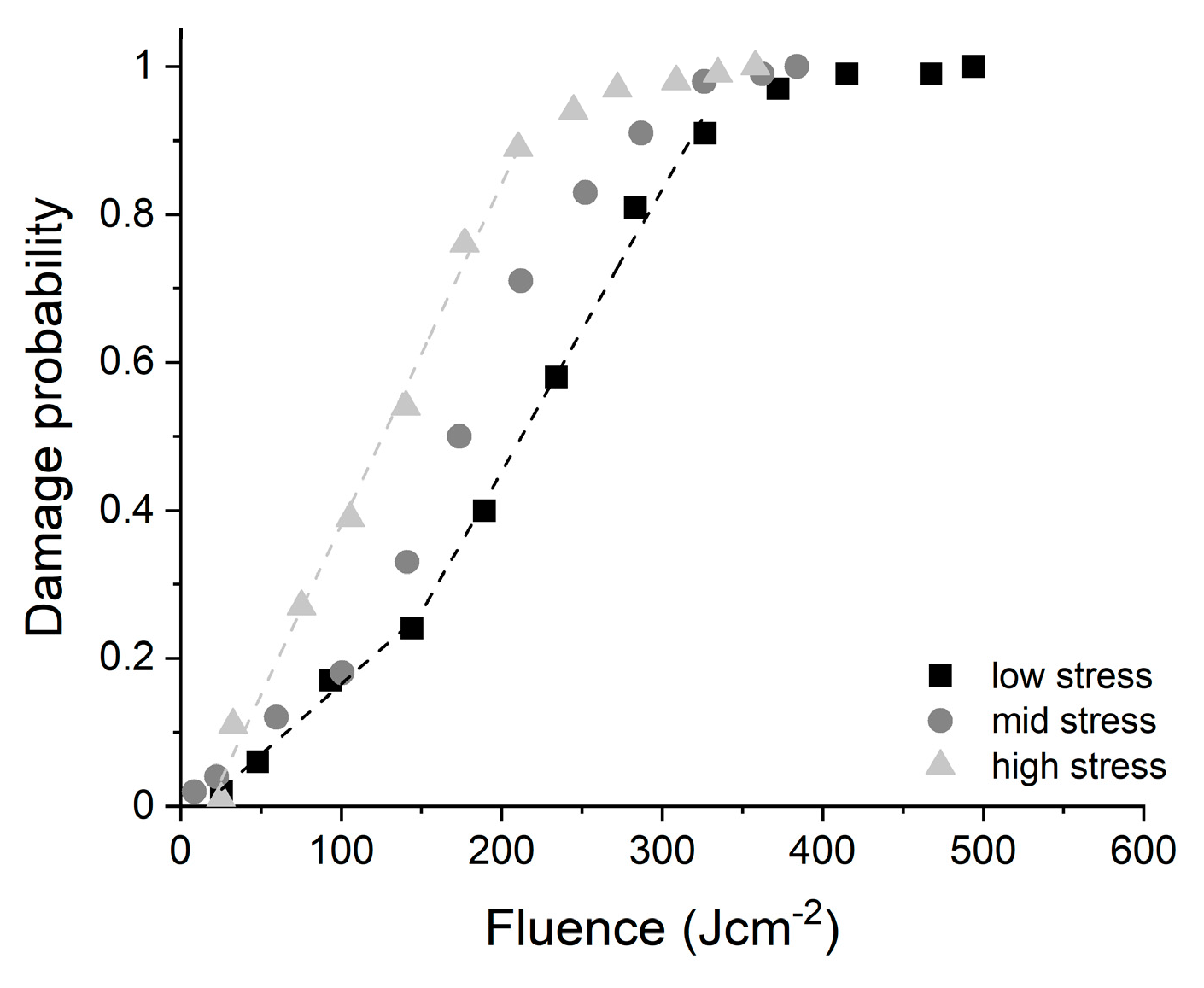
LIDT measurements were performed on 480 nm HfO2 layers with low stress (≈0.5 GPa), medium stress (≈1.5 GPa), as well as high-stress level (≈3 GPa) deposited on fused silica.
Figure 4 shows the estimated damage probability of these samples as a function of the laser fluence. A single slope characterizes the high-stress case, while the moderate and lower stress cases are composed of two parts—a less steep initial part followed by a second part with a similar slope as the high stress.
In other words, the zero damage probability is independent of the stress state; however, the 0.5 damage probability is achieved at much lower fluence for the moderately and highly stressed sample. The same is true for the damage probability of 1.
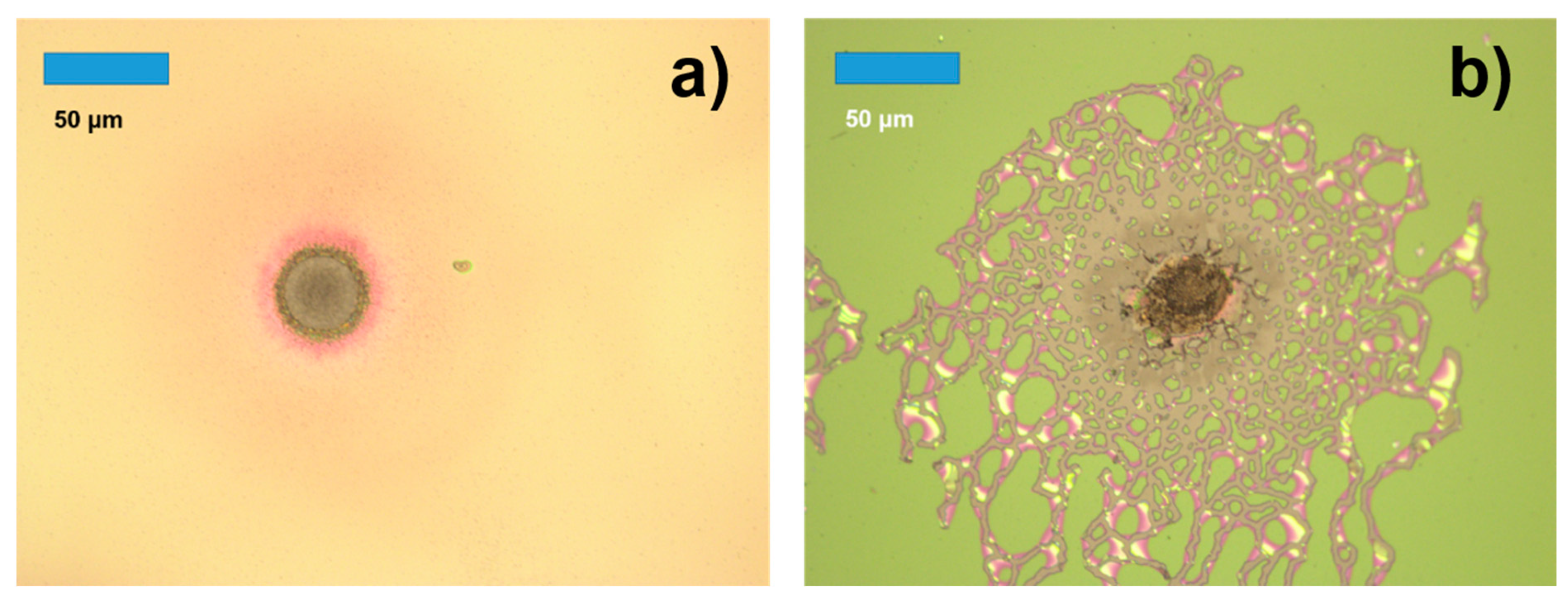
Figure 5 shows typical pictures of damaged sites for low-stress and high-stress samples, respectively. The low-stress samples (Figure 5a) show a clear, finite plasma scald-type damage morphology with dimensions similar to the laser beam size. In contrast to this, the high-stress samples (Figure 5b) show the irradiated spot but surrounded by a large cracked area.

4. Discussion

Comparing the results of the X-ray analysis with the stress measurements, it turns out that bombarding of HfO2 during film growth with high-energy oxygen particles leads to stress-induced crystallization similar to annealing of HfO2 films [19]. Investigation of rapid thermal annealing of HfO2 films shows thickness reduction (i.e., volume reduction) when the films undergo the amorphous to crystalline transition [18]. Thus, the effect of the secondary ion beam is twofold. On the one hand, it densifies the film, which leads to stress build-up. On the other hand, the kinetic energy and/or the stress creates favorable conditions for the crystallization, which can reduce part of the stress. After full crystallization, further densification cannot be compensated for anymore. As a consequence, the films crack and delaminate.
The macroscopic cracking/delamination and eventual blistering can explain why we observed a sharp decline in the net stress, which is not expected according to the Davis or Bilek–McKenzie models [9,10].
The structure zone diagram (SZD), which takes the generalized deposition temperature, the ion energy as well as the film thickness into account [20] can characterize the deposition of thin films. In the case of Uassist = 0, only the primary sputtered molecules from the target reach the specimen surface. A few tens of eV energy characterize these species at most. The substrate temperature is most probably close to the set 100 °C (~0.1 Tm for HfO2), and thus the deposition takes place at the border of Zone 1 and Zone T. The mean free path for oxygen molecules and argon atoms for an operating pressure of 3.5 × 10⁻⁴ torr is larger than the assisting source–substrate distance, thus most of the species reach the specimen without any energy loss. Accordingly, a deposition at the border of Zone T and Zone 3 takes place. This is in agreement with the observed crystallization of the layers.
As is observed for ion implantation and amorphization of crystals for waveguide creation, as well as the annealing of HfO2 films, the amorphous material exhibits a lower refractive index compared to the crystal phase [21,22]. This is in contrast to our measurements where amorphous films have a higher refractive index. The fact that the refractive index is very sensitive to structural changes may explain why the decrease could be a consequence of nano cracks that are not visible in microscopy inspection.
As for the LIDT with 1064 nm wavelength, nanosecond laser pulses on IBS and e-beam deposited films indicate that the laser irradiation causes damage via thermal-induced stress, e.g., [23,24]. We observed the expected behavior, and due to the cracks, the highly stressed HfO2 is characterized by a lower LIDT.

5. Conclusions

In this report, we present the influence of a second ion beam source and the ion beam voltage on film stress, optical properties, film structure, and LIDT of HfO2-films deposited with ion beam sputtering. It was found that bombarding the growing film with energetic ions increases thin-film stress, which leads to crystallization. Nevertheless, due to the high stress, the films show a reduced LIDT value as compared to the “benchmark” low-stress films.

Author Contributions

I.S.: main investigator; Z.B.-M., V.J.W., T.G.: support in experiments; Z.B.-M.: writing—draft preparation; A.B., V.J.W., T.S., T.G.: writing—review and editing; Z.B.-M., A.B., A.S., T.S., T.G.: supervision. All authors have read and agreed to the published version of the manuscript.

Funding

This research was founded by a private foundation from Liechtenstein.

Institutional Review Board Statement

Not applicable.

Informed Consent Statement

Not applicable.

Data Availability Statement

The data presented in this study are available on request from the corresponding author.

Conflicts of Interest

The authors declare no conflict of interest.

References

  1. Kaiser, N.; Pulker, H.K. Optical Interference Coatings; Springer: Berlin, Germany, 2003. [Google Scholar]
  2. Ristau, D. Laser-Induced Damage in Optical Materials; CRC Press: Boca Raton, FL, USA, 2014. [Google Scholar]
  3. Langdon, B.; Patel, D.; Krous, E.; Rocca, J.J.; Menoni, C.S.; Tomasel, F.; Kholi, S.; McCurdy, P.R.; Langston, P.; Ogloza, A. Influence of process conditions on the optical properties HfO2/SiO2 thin films for high power laser coatings. In Laser-Induced Damage in Optical Materials: 2007; SPIE: Bellingham, WA, USA, 2007; Volume 6720, p. 67200X. [Google Scholar]
  4. Liu, H.; Jiang, Y.; Wang, L.; Li, S.; Yang, X.; Jiang, C.; Liu, D.; Yi-Qin, J.; Zhang, F.; Chen, D. Effect of heat treatment on properties of HfO2 film deposited by ion-beam sputtering. Opt. Mater. 2017, 73, 95–101. [Google Scholar] [CrossRef]
  5. Stolz, C.J.; Thomas, M.D.; Griffin, A.J. BDS thin film damage competition. In Laser-Induced Damage in Optical Materials: 2008; SPIE: Bellingham, WA, USA, 2008; Volume 7132, p. 71320. [Google Scholar] [CrossRef]
  6. Gusev, E.; Cartier, E.; Buchanan, D.; Gribelyuk, M.; Copel, M.; Schmidt, H.; D’Emic, C. Ultrathin high-K metal oxides on silicon: Processing, characterization and integration issues. Microelectron. Eng. 2001, 59, 341–349. [Google Scholar] [CrossRef]
  7. Choi, J.; Mao, Y.; Chang, J. Development of hafnium based high-k materials—A review. Mater. Sci. Eng. R Rep. 2011, 72, 97–136. [Google Scholar] [CrossRef]
  8. Cevro, M.; Carter, G. Ion beam sputtering and dual ion beam sputtering of titanium oxide films. J. Phys. D Appl. Phys. 1995, 28, 1962–1976. [Google Scholar] [CrossRef]
  9. Davis, C. A simple model for the formation of compressive stress in thin films by ion bombardment. Thin Solid Films 1993, 226, 30–34. [Google Scholar] [CrossRef]
  10. Bilek, M.M.M.; McKenzie, D.R. A comprehensive model of stress generation and relief processes in thin films deposited with energetic ions. Surf. Coatings Technol. 2006, 200, 4345–4354. [Google Scholar] [CrossRef]
  11. Bischoff, M.; Nowitzki, T.; Voß, O.; Wilbrandt, S.; Stenzel, O. Postdeposition treatment of IBS coatings for UV applications with optimized thin-film stress properties. Appl. Opt. 2014, 53, A212–A220. [Google Scholar] [CrossRef] [PubMed]
  12. Rammula, R.; Aarik, J.; Mändar, H.; Ritslaid, P.; Sammelselg, V. Atomic layer deposition of HfO2: Effect of structure development on growth rate, morphology and optical properties of thin films. Appl. Surf. Sci. 2010, 257, 1043–1052. [Google Scholar] [CrossRef]
  13. Wei, Y.; Xu, Q.; Wang, Z.; Liu, Z.; Pan, F.; Zhang, Q.; Wang, J. Growth properties and optical properties for HfO2 thin films deposited by atomic layer deposition. J. Alloys Compd. 2018, 735, 1422–1426. [Google Scholar] [CrossRef]
  14. Stenzel, O.; Wilbrandt, S.; Kaiser, N.; Vinnichenko, M.; Munnik, F.; Kolitsch, A.; Chuvilin, A.L.; Kaiser, U.; Ebert, J.; Jakobs, S.; et al. The correlation between mechanical stress, thermal shift and refractive index in HfO2, Nb2O5, Ta2O5 and SiO2 layers and its relation to the layer porosity. Thin Solid Films 2009, 517, 6058–6068. [Google Scholar] [CrossRef]
  15. Yoon, S.; Kang, S.; Jung, W.; Kim, S.-W.; Yoon, D. Effect of assist ion beam voltage on intrinsic stress and optical properties of Ta2O5 thin films deposited by dual ion beam sputtering. Thin Solid Films 2008, 516, 3582–3585. [Google Scholar] [CrossRef]
  16. Hopcroft, M.; Nix, W.D.; Kenny, T.W. What is the Young’s Modulus of Silicon? J. Microelectromech. Syst. 2010, 19, 229–238. [Google Scholar] [CrossRef] [Green Version]
  17. Gischkat, T.; Schachtler, D.; Balogh-Michels, Z.; Botha, R.; Mocker, A.; Eiermann, B.; Günther, S. Influence of ultra-sonic frequency during substrate cleaning on the laser resistance of antireflection coatings. In Laser-induced Damage in Optical Materials 2019; SPIE: Bellingham, WA, USA, 2019; Volume 11173, p. 1117317. [Google Scholar]
  18. Botha, R.; Bischof, D.; Vetsch, B.; Scherrer, U.; Michler, M.; Rinner, S.; Ettemeyer, A.; Ziolek, C. Investigation of the ageing effects exhibited by AR coatings exposed to ultraviolet laser irradiation. In Laser-Induced Damage in Optical Materials 2016; SPIE: Bellingham, WA, USA, 2016; Volume 10014, p. 100141L. [Google Scholar] [CrossRef]
  19. Fu, W.-E.; Chang, C.-W.; Chang, Y.-Q.; Yao, C.-K.; Liao, J.-D. Reliability assessment of ultra-thin HfO2 films deposited on silicon wafer. Appl. Surf. Sci. 2012, 258, 8974–8979. [Google Scholar] [CrossRef]
  20. Anders, A. A structure zone diagram including plasma-based deposition and ion etching. Thin Solid Films 2010, 518, 4087–4090. [Google Scholar] [CrossRef] [Green Version]
  21. Tan, T.; Liu, Z.; Lu, H.; Liu, W.; Tian, H. Structure and optical properties of HfO2 thin films on silicon after rapid thermal annealing. Opt. Mater. 2010, 32, 432–435. [Google Scholar] [CrossRef]
  22. Wesch, W.; Wendler, E. Ion Beam Modification of Solids; Springer Series in Surface Science 61; Springer: Cham, Switzerland, 2016. [Google Scholar]
  23. Yao, J.; Shao, J.; He, H.; Fan, Z. Effects of annealing on laser-induced damage threshold of TiO2/SiO2 high reflectors. Appl. Surf. Sci. 2007, 253, 8911–8914. [Google Scholar] [CrossRef]
  24. Abromavičius, G.; Kičas, S.; Buzelis, R. High temperature annealing effects on spectral, microstructural and laser damage resistance properties of sputtered HfO2 and HfO2-SiO2 mixture-based UV mirrors. Opt. Mater. 2019, 95, 109245. [Google Scholar] [CrossRef]
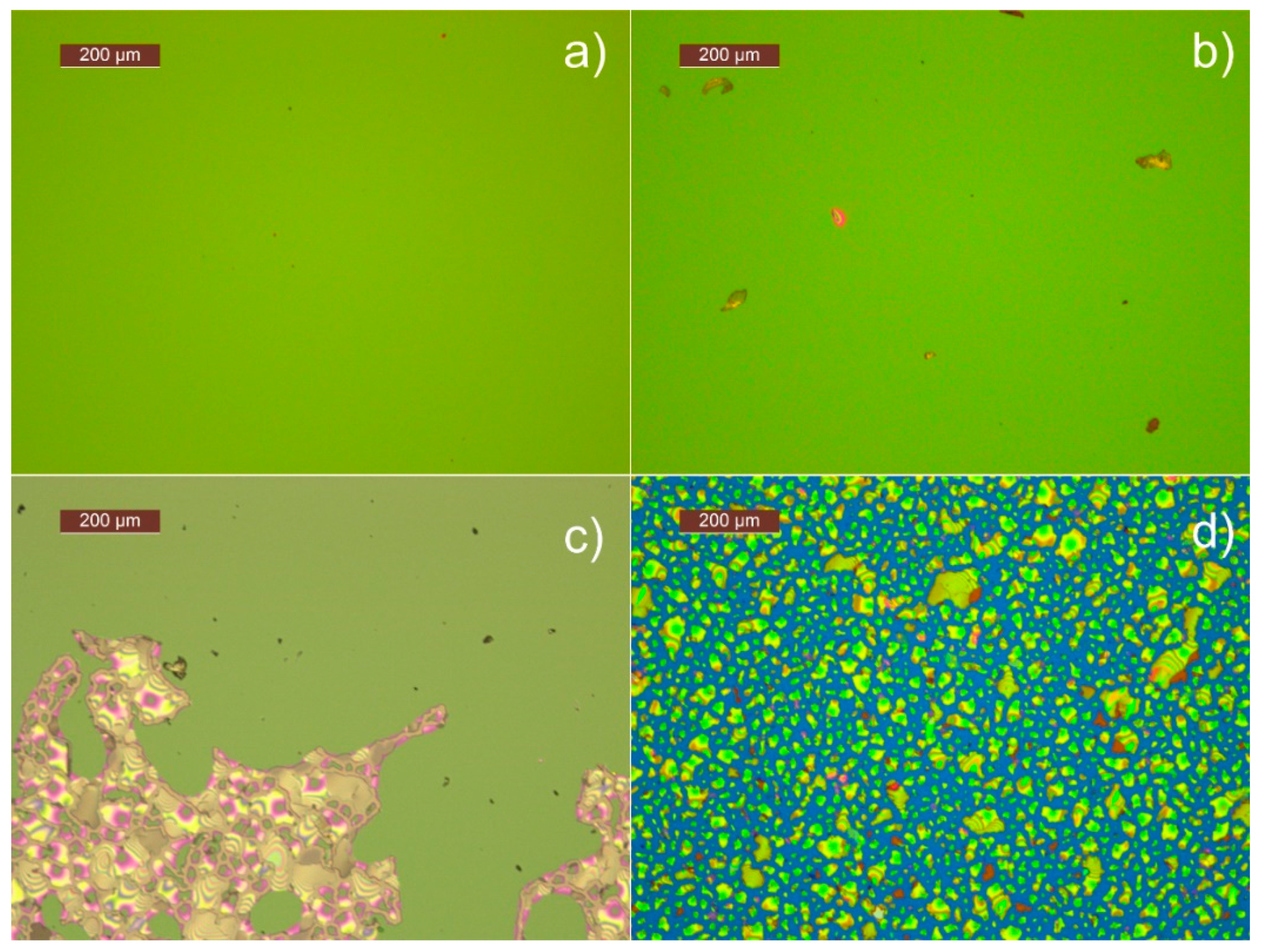
Figure 1. The state of the HfO2 films for different assisting source voltages (ad): 0, 250, 575, and 600 V, respectively. At low ion energies, only an increase in the large-scale defect concentration is observable (b); however, higher voltages lead to partial delamination or complete blistering (c,d).
Applsci 11 00189 g001
Figure 2. (a) The refractive index (n) and the extinction coefficient (k) at 633 nm as a function of the assist source voltage. The dashed lines are a 4th order polynomial fit and linear fit of the data, respectively. (b) Grazing incidence XRD on the HfO2 layers produced by different assisting beam voltage.
Applsci 11 00189 g002
Figure 3. (a) Calculated film stress for Si-substrates coated with 480 nm HfO2 at 100 °C as function of the beam voltage of the assisting ion beam source. The dashed line is a spline fit of the data. (b) Fitted stress curves as a function of beam voltage of the assisting ion beam source for 100 nm as well as 480 nm HfO2 films.
Applsci 11 00189 g003
Figure 4. The laser-induced damage (LIDT) curves for low- (0.5 GPa), moderate (1.5 GPa), and high-stress (3 GPa) specimens.
Applsci 11 00189 g004
Figure 5. Damage sites for (a) low- and (b) high-stress samples.
Applsci 11 00189 g005
Table 1. Summary of the deposition parameters for the sputtering of the HfO2 layers.
SeriesLayer ThicknessAssisting Ion Beam Source
[nm]Uassist [V]Iassist [mA]
A48000
250, 450100
550, 575150
590160
600166
650183
700200
B10000
450100
550150
600166
Publisher’s Note: MDPI stays neutral with regard to jurisdictional claims in published maps and institutional affiliations.