Article

A Directly Modulated Laterally Coupled Distributed Feedback Laser Array Based on SiO2 Planarization Process

1
Beijing National Research Centre for Information Science and Technology, Department of Electronic Engineering, Tsinghua University, Beijing 100084, China
2
Center for Flexible Electronics Technology, Tsinghua University, Beijing 100084, China
3
Flexible Intelligent Optoelectronic Device and Technology Center, Institute of Flexible Electronics Technology of THU, Jiaxing 314006, China
*
Authors to whom correspondence should be addressed.
Appl. Sci. 2021, 11(1), 221; https://doi.org/10.3390/app11010221
Submission received: 8 December 2020 / Revised: 19 December 2020 / Accepted: 25 December 2020 / Published: 29 December 2020
(This article belongs to the Special Issue Novel and Highly Efficient Semiconductor-Based Light Sources)

Abstract

:
Low-cost and high-speed single-mode semiconductor lasers are increasingly required as wide-band access fiber communication expands in recent years. Here, a high-speed laterally coupled distributed feedback (LC-DFB) laser array is achieved based on a SiO2 planarization process. The device exhibits low threshold currents of about 12 mA and high slope efficiencies over 0.26 W/A. Stable single mode operation and high-speed performance are realized with side mode suppression ratios (SMSR) over 45 dB, and 3-dBe bandwidths exceed 14 GHz for all four channels. Such a high-speed and process simple LC-DFB laser array shows great potential to the low-cost fiber communication networks.

1. Introduction

High-speed optical communication develops rapidly with the rapid increase of the amount of data. Low-cost and high-performance laser sources, such as distributed feedback (DFB) laser sources, are urgently needed. Various high-speed DFB lasers were demonstrated [1,2], but most of them require at least one epitaxial regrowth step after grating definition and thus have complicated process and high fabrication costs.
Laterally coupled (LC) DFB lasers use surface gratings beside the ridge waveguide to select longitudinal mode; thus, they circumvent the complex regrowth step and have the potential for low-cost fiber communication applications. LC-DFB lasers with good static performance, e.g., side mode suppression ratio (SMSR), were reported [3,4,5,6]. However, there are only a few reports about the high frequency performance, e.g., modulation bandwidth [7,8,9]. It is actually a trade-off between the single mode performance and the modulated bandwidth, and it is especially challenging to achieve a high modulation bandwidth for LC-DFB lasers, which often suffer from a low coupling coefficient and thus have a long cavity to select longitudinal mode.
In this paper, a high-speed LC-DFB laser array with deep and planar lateral gratings is demonstrated. We have developed a SiO2 planarization process to simplify the fabrication. The array exhibits low threshold currents of about 12 mA, high slope efficiencies over 0.26 W/A and high SMSRs over 45 dB. The 3-dBe small-signal modulation bandwidths exceed 14 GHz for all four channels under injection currents of 100 mA. Such an LC-DFB laser array is very promising for applications of high-speed and low-cost optical communication.

2. Device Structure, Design and Fabrication Methods

Figure 1a depicts the schematic of the proposed LC-DFB laser array in which laterally coupled gratings are along both sides of the ridge waveguide to provide both lateral optical confinement and longitudinal feedback. A 2-μm-thick SiO2 dielectric layer supports the planar electrodes and passivates the side wall of ridge waveguides. A p-type electrode pad with a diameter of 100 μm introduces a pad capacitance C of 0.18 pF.
The intrinsic modulation speed of DMLs is limited by the relaxation oscillation frequency ( f r ). The f r is given by [10].
f r = ( Γ ν g a η i q V ) ( I I t h ) 2 π = D ( I I t h )
where Γ is the active region optical confinement factor, ν g is the group velocity, a = g / N [11] is the differential gain, η i is the internal quantum efficiency, and I and I t h are the bias current and the threshold current, respectively. q is the elementary charge, and V is the active volume. The D factor D = 1 / 2 π ( Γ ν g a η i ) / ( q V ) describes the slope of f r on the square root of the bias current above the threshold [12].
Strained multi-quantum wells (MQWs) were designed for high speed modulations which considered the improving of the differential gain a [13]. The epitaxial structure is the same as Li, A.K., which consists of five periods of 5-nm-thick InGaAlAs quantum-well and 8.5-nm-thick InGaAlAs barrier [14]. The optical confinement factor of the active region Γ is also an important parameter for f r . The relationship of the coupling coefficient κ and Γ versus the ridge width are calculated by the finite element analysis (FEA) method as shown in Figure 1b. The optical confinement factor Γ increases with the width of the waveguide, yet a narrow waveguide is needed for an LC-DFB to increase the grating coupling coefficient κ. A narrow waveguide would result in more power leakage out of the waveguides, thus decreasing Γ . However, it enhances the optical field in the grating region and increases κ . The strength of the grating’s feedback is described by the normalized coupling coefficient (κL). The cavity length is inverse to κ when κL is a constant. The f r is proportional to the κ and Γ by Equation (1). The ridge width is designed as 1.2 μm considering a compromise between κ and Γ . Figure 1c shows the variation of κ versus duty cycle γ assuming a ridge width of 1.2 μm and a grating order of 3. A duty cycle of 0.9 is designed to obtain a higher κ taking the etching broadening effect into account.
To fabricate the deep lateral gratings, the pattern was formed by electron beam lithography (EBL) on 400-nm-thick HSQ photo-resist. Deep lateral gratings were formed by inductively coupled plasma (ICP) etching with CH4/H2/Ar gas mixture. Finally, diluted hydrochloric acid solution was adopted to smooth the side wall of lateral gratings, whose microscope image captured by scanning electron microscope (SEM) is shown in Figure 2a. The lateral gratings along the 1.2-μm-wide strips have pitches of 599.7, 602, 604 and 606.7 nm, a duty factor ~0.75 and a grating depth ~1.75 μm, which results in the coupling coefficient κ ~ 30 cm−1 according to the finite element analysis (FEA) simulation, as shown in Figure 1c.
After the process of the deep gratings and waveguides, a planarization process of silica was adopted instead of a benzocyclobutene (BCB) planarization process described in the article of Li, A.K. The process was significantly simplified as shown in Figure 3. A 2-μm-thick SiO2 supporting layer was deposited by PECVD, whose surface topography is shown in Figure 2b. SiO2 on top of the ridge waveguide was removed by CHF3 ICP after self-alignment exposure, as shown in Figure 2c. Then Ti/Pt/Au p-type electrodes and Ti/Au n-type electrodes were deposited, respectively. Laser chips with a cavity length of ~350 μm were cleaved out of the wafer. High reflection (HR) film with reflectivity of 98.66% and anti-reflection (AR) film with reflectivity of 0.37% were deposited on two ends of lasers respectively by evaporation after annealing to increase the output power of the facet.

3. Results and Discussion

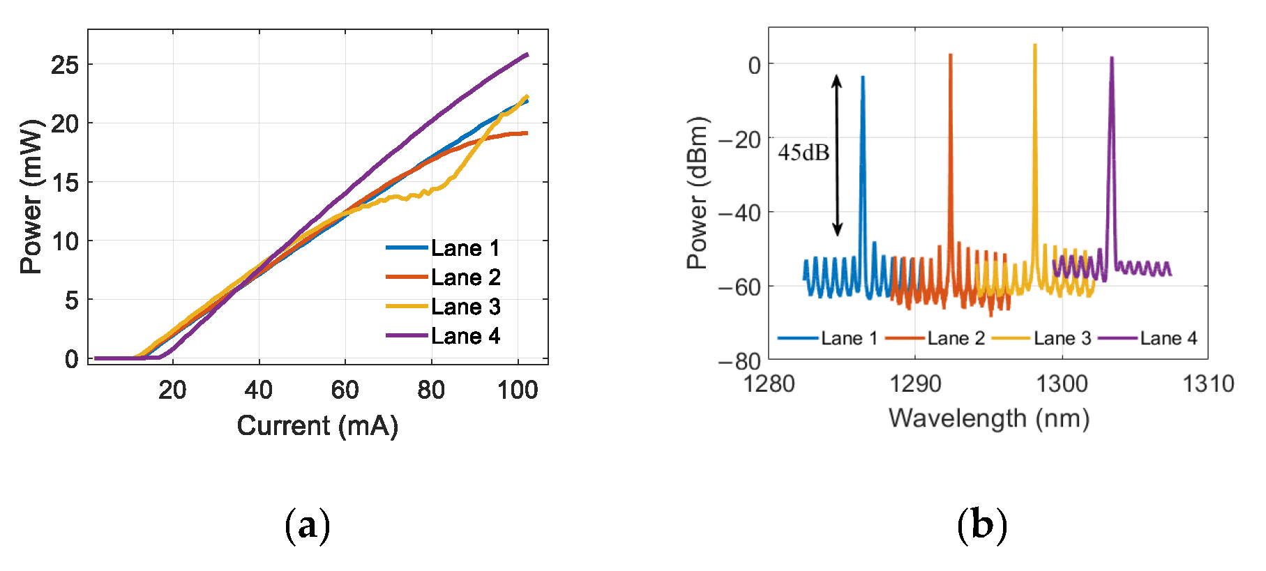
The lasing characteristics were tested at 10 °C under continuous-wave conditions. Figure 4a shows the typical fiber coupled output power as a function of injection currents for a four-channel LC-DFB laser array. The threshold currents are about 12 mA. Excellent slope efficiencies of above 0.26 W/A are achieved for all channels. The output power is about 20 mW at an injection current of 100 mA. Such excellent output power performance for LC-DFB lasers is attributed to the combination of a good epitaxy of AlGaInAs wafer and HR-AR facet coated. The four-channel wavelengths range from 1286 nm to 1303 nm with a channel spacing of about 1 THz, as shown in Figure 4b. An average SMSR exceeding 50 dB is obtained, which is comparable to that of conventional DFB lasers, indicating the good longitudinal mode selectivity of deep and planar lateral gratings.
The DML array is p-side up soldered onto a copper block to improve the thermal characteristics. The p-type electrode is bonded to a AlN microstrip transmission line by gold wires through a matching resistor of 35 Ω . The 3-dBe bandwidths of the small-signal modulation response shown in Figure 5 exceed 14 GHz for all four channels. A bandwidth of about 18 GHz is obtained on lane 3 under an injection current of 100 mA. To our knowledge, this is the best small-signal modulation performance for LC-DFB lasers. The frequency response of the laser can be fitted as follows [15], in which the junction capacitance is taken into account:
| H ( f ) | = | f r 2 ( f r 2 f 2 ) 2 + ( γ 2 π f ) 2 | | 1 1 + f / f P N | | 1 1 + ( f / f R C ) 2 |
Here γ is the damping factor. The f P N and f R C are the cut-off frequencies caused by the junction capacitance, the contact capacitance and the series resistance. Figure 6a shows the relationships between f r and the square root of the bias currents above the threshold for four channels. The D factors of the four-channel lasers are 1.56, 1.6, 1.49 and 1.23 GHz/mA1/2, respectively. The values of the four-channel differential gain a are obtained from the D factors, as shown in Figure 6b. The differential gain tends to decrease with the increase of the lasing wavelength. Generally, a lasing wavelength shorter than the material peak gain provides a larger differential gain. The maximum appears at the 5 nm detuned grating wavelength to longer wavelengths with respect to the material peak gain, which is about 1285 nm.

4. Conclusions

A high-speed LC-DFB laser array based on a SiO2 planarization process is demonstrated. Each channel exhibits a low threshold current of about 12 mA and a high slope efficiency over 0.26 W/A. Stable single mode operation is demonstrated with SMSRs over 45 dB. The small-signal 3-dBe bandwidths exceed 14 GHz for all four channels under injection currents of 100 mA. The high modulation bandwidth benefits from high differential gain, and it can be further improved with a shorter cavity. Such results imply that the LC-DFB laser array can combine high efficiency slopes, high SMSRs, high modulation bandwidths and a simple fabrication process, and it shows great potential to low-cost optical communication.

Author Contributions

Conceptualization, J.W. and Y.L.; data curation, Q.W.; formal analysis, Q.W.; funding acquisition, Y.L.; investigation, Q.W. and J.W.; methodology, Q.W. and C.S.; project administration, Y.L.; resources, C.S. and Y.H.; supervision, Y.L.; validation, B.X., Z.H., L.W., H.L. and J.Y.; visualization, Q.W.; writing—original draft, Q.W.; writing—review and editing, Q.W. and J.W. All authors have read and agreed to the published version of the manuscript.

Funding

This research was funded by the National Key Research and Development Program (Grant No. 2017YFA0205800); the Science Challenge Project (Grant No. TZ2016003); the National Natural Science Foundation of China (Grant No. 51561165012, 51561145005, 61574082, 61621064, 61822404, 61875104, 61904093, 61927811); Tsinghua University Initiative Scientific Research Program (Grant No. 20161080068, 20161080062); the China Postdoctoral Science Foundation (Grant No. 2018M640129, 2019T120090) and the Collaborative Innovation Centre of Solid-State Lighting and Energy-Saving Electronics.

Institutional Review Board Statement

Not applicable.

Informed Consent Statement

Not applicable.

Data Availability Statement

The data that support the plots within this paper and other findings of this study are available from the corresponding author upon reasonable request.

Conflicts of Interest

The authors declare no conflict of interest.

References

  1. Nakahara, K.; Wakayama, Y.; Kitatani, T.; Taniguchi, T.; Fukamachi, T.; Sakuma, Y.; Tanaka, S. Direct Modulation at 56 and 50 Gb/s of 1.3-μm InGaAlAs Ridge-Shaped-BH DFB Lasers. IEEE Photonics Technol. Lett. 2014, 27, 534–536. [Google Scholar] [CrossRef]
  2. Liu, G.; Zhao, G.; Sun, J.; Gao, D.; Lu, Q.; Guo, W. Experimental demonstration of DFB lasers with active distributed reflector. Opt. Express 2018, 26, 29784–29795. [Google Scholar] [CrossRef] [PubMed]
  3. Kim, H.-C.; Wiedmann, J.; Matsui, K.; Tamura, S.; Arai, S. 1.5-m-wavelength distributed feedback lasers with deeply etched first-order vertical grating. Jpn. J. Appl. Phys. 2001, 40, L1107. [Google Scholar] [CrossRef]
  4. Tolstikhin, V.I.; Watson, C.D.; Pimenov, K.; Moore, R.; Logvin, Y.; Wu, F. Laterally coupled DFB lasers for one-step growth photonic integrated circuits in InP. IEEE Photonics Technol. Lett. 2009, 21, 621–623. [Google Scholar] [CrossRef]
  5. Telkkälä, J.; Viheriälä, J.; Bister, M.; Karinen, J.; Melanen, P.; Dumitrescu, M.; Guina, M. Narrow linewidth 1.55 µm laterally-coupled DFB lasers fabricated using nanoimprint lithography. In Proceedings of the IPRM 2011-23rd International Conference on Indium Phosphide and Related Materials, Institute of Electrical and Electronics Engineers, Berlin, Germany, 22 May 2011; pp. 1–4. [Google Scholar]
  6. Tang, S.; Hou, L.; Chen, X.; Marsh, J.H. Multiple-wavelength distributed-feedback laser arrays with high coupling coefficients and precise channel spacing. Opt. Lett. 2017, 42, 1800–1803. [Google Scholar] [CrossRef] [PubMed] [Green Version]
  7. Schreiner, R.; Schweizer, H. High-frequency operation of 1.57-μm laterally coupled distributed feedback lasers with self-aligned Ohmic contacts and nickel surface gratings. IEEE J. Select Top Quantum Electron. 2003, 9, 1179–1182. [Google Scholar] [CrossRef]
  8. Afzal, S.; Schnabel, F.; Scholz, W.; Reithmaier, J.P.; Gready, D.; Eisenstein, G.; Vallone, M. 1.3-μm Two-Section DBR Lasers Based on Surface Defined Gratings for High-Speed Telecommunication. IEEE Photonics Technol. Lett. 2011, 23, 411–413. [Google Scholar] [CrossRef]
  9. Uusitalo, T.; Virtanen, H.; Bardella, P. Dumitrescu, M. Analysis of the photon–photon resonance influence on the direct modulation bandwidth of dual-longitudinal-mode distributed feedback lasers. Opt. Q. Electron. 2017, 49, 46. [Google Scholar] [CrossRef]
  10. Coldren, L.A.; Corzine, S.W.; Masanovic, M.L. A Phenomenological Approach to Diode Lasers. In Diode Lasers and Photonic Integrated Circuits, 2nd ed.; John Wiley & Sons, Inc.: Hoboken, NJ, USA, 1995; p. 73. [Google Scholar]
  11. Coldren, L.A.; Corzine, S.W.; Masanovic, M.L. Dynamic Effects. In Diode Lasers and Photonic Integrated Circuits, 2nd ed.; John Wiley & Sons, Inc.: Hoboken, NJ, USA, 1995; p. 258. [Google Scholar]
  12. Matsuo, S.; Kakitsuka, T. Low-operating-energy directly modulated lasers for short-distance optical interconnects. Adv. Opt. Photonics 2018. [Google Scholar] [CrossRef]
  13. Liu, G.; Chuang, S.L. High-speed modulation of long-wavelength In(1−x)GaxAsyP(1−y) and In(1−x−y)Gax AlyAs strained quantum-well lasers. IEEE J. Quantum Elect. 2001, 37, 1283–1291. [Google Scholar] [CrossRef]
  14. Li, A.; Wang, J.; Sun, C.; Wang, Y.; Yang, S.; Xiong, B.; Luo, Y.; Hao, Z.B.; Han, Y.J.; Wang, L.; et al. 1.3 μm 10-Wavelength Laterally Coupled Distributed Feedback Laser Array with High-Duty-Ratio Gratings. Phys. Status Solid 2018, 215, 1800490. [Google Scholar] [CrossRef] [Green Version]
  15. Olshansky, R.; Hill, P.; Lanzisera, V.; Powzainik, W. Frequency response of 1.3 µm InGaAsP high speed semiconductor lasers. IEEE J. Quantum Electron. 1987, 23, 1410–1418. [Google Scholar] [CrossRef]
Figure 1. (a) Schematic of the structure of the laterally coupled distributed feedback (LC-DFB) laser array with deep and planar lateral gratings. (b) κ (blue line) and Γ (red line) versus the ridge width with the third order gratings and a duty factor of 0.5. (c) κ as a function of the duty cycle γ on third order gratings with a ridge width of 1.2 μm.
Applsci 11 00221 g001
Figure 2. (a) SEM image of the as-etched waveguide and lateral gratings. (b) Surface topography of the SiO2 supporting layer. (c) SEM image of the waveguide and lateral gratings after removing SiO2 on top of the current injection region.
Applsci 11 00221 g002
Figure 3. The comparison diagram of (a) BCB planarization process and (b) SiO2 planarization process.
Applsci 11 00221 g003
Figure 4. (a) Fiber coupled output power as a function of injection currents (L-I) of the LC-DFB laser array with the operating temperature at 10 °C. (b) The lasing spectra under injection currents of 100 mA at 10 °C.
Applsci 11 00221 g004
Figure 5. Small-signal frequency responses of the LC-DFB laser array with injection currents of 100 mA at 10 °C.
Applsci 11 00221 g005
Figure 6. (a) The relationship between the relaxation oscillation frequency f r and the square root of the bias current above the threshold, where the solid dots and lines are the experimental data and fitting results, respectively. (b) The relationship between the values of four-channel differential gain and lasing wavelengths.
Applsci 11 00221 g006
Publisher’s Note: MDPI stays neutral with regard to jurisdictional claims in published maps and institutional affiliations.