Article

Solution-Processed Memristor Devices Using a Colloidal Quantum Dot-Polymer Composite

1
School of Advanced Materials Science and Engineering, Sungkyunkwan University, Suwon 16419, Korea
2
Department of Advanced Materials, Kyonggi University, Suwon 16227, Korea
*
Authors to whom correspondence should be addressed.
These authors contributed equally to this work.
Appl. Sci. 2021, 11(11), 5020; https://doi.org/10.3390/app11115020
Submission received: 7 April 2021 / Revised: 27 May 2021 / Accepted: 27 May 2021 / Published: 28 May 2021
(This article belongs to the Special Issue Colloidal Quantum Dot Based Electric and Optoelectronic Devices)

Abstract

:
In this study, we demonstrate solution-processed memristor devices using a CdSe/ZnS colloidal quantum dot (CQD)/poly(methyl methacrylate) (PMMA) composite and their electrical characteristics were investigated. Particularly, to obtain stable memristive characteristics with a large current switching ratio, the concentration of CdSe/ZnS QDs in the PMMA matrix was optimized. It was found that with the CdSe/ZnS QD concentration of 1 wt%, the memristor device exhibited a high current switching ratio of ~104 and a retention time over 104 s, owing to the efficient charge trapping and de-trapping during the set and reset processes, respectively. In addition, we investigated the operational stability of the device by carrying out the cyclic endurance test and it was found that the memristor device showed stable switching behavior up to 400 cycles. Furthermore, by analyzing the conduction behavior of the memristor device, we have deduced the possible mechanisms for the degradation of the switching characteristics over long switching cycles. Specifically, it was observed that the dominant conduction mechanism changed from trap-free space charge-limited current conduction to trap charge-limited current conduction, indicating the creation of additional trap states during the repeated operation, disturbing the memristive operation.

1. Introduction

Recently, memristors have received significant interest for next-generation electronics such as neuromorphic computing systems, owing to their potential advantages such as high energy efficiency, good scalability, and compatibility with conventional complementary metal-oxide-semiconductor fabrication processes [1,2,3,4,5,6,7,8,9,10]. Particularly, memristors are considered as the fourth fundamental non-linear circuit element linking charge and magnetic flux [11]. In the memristor device, the electrical resistance state can be changed according to the history of the external stimulation, such as the voltage pulses, allowing the emulation of learning behavior and various neuromorphic functions. To realize the memristor device, various material systems have been investigated including ferroelectrics [12], ferromagnetics [13], and phase-changing materials [4,14]. In addition, organic/inorganic hybrid materials have received much attention recently due to their wide tunability in electrical properties, good mechanical flexibility, low-temperature process, and large-area scalability [15,16]. Moreover, since the organic/inorganic hybrids can be deposited by a simple solution process, the use of sophisticated vacuum deposition processes can be omitted, enabling the realization of cost-effective and area-scalable neuromorphic systems.
In the case of organic/inorganic hybrid-based memristors, it is claimed that the inorganic components such as the metallic or semiconducting nanoparticles play an important role in regulating the resistance state by acting as charge storage or charge trapping centers [17,18]. For the inorganic component, colloidal quantum dots (CQDs) can be a good candidate since they are solution processable and their bandgap can be tuned by adjusting the size of the QDs [19,20]. Particularly, when the QDs are embedded in an insulating polymer with a large bandgap over 3 eV [21], effective charge trapping can be expected at the QDs due to the relatively small bandgap of the QDs. Moreover, the QD-polymer memristors can provide potential advantages such as good mechanical flexibility [22], high optical transparency, and low voltage operation for efficient energy consumption [20]. To date, although some research has been carried on QD-polymer-based memristors [23], there is still a need for optimizing the QD concentration since the trapping and de-trapping of charge carriers at the QDs largely affect the memristive characteristics. Furthermore, a study on the conduction mechanism is required to understand the dominant conduction mechanism of the QD-polymer-based memristors and the possible origin of the degradation mechanisms under repeated operations.
In this study, we demonstrate solution-processed memristor devices using a CdSe/ZnS QD-poly(methyl methacrylate) (PMMA) composite, and their electrical characteristics were investigated. Particularly, to obtain stable memristive characteristics, we optimized the concentration of CdSe/ZnS QDs in the PMMA matrix. The CdSe/ZnS QD:PMMA memristor with an optimized QD ratio exhibited decent memristive characteristics with a high current switching ratio up to ~104 and a relatively long retention time over 104 s. In addition, the operational stability of the device was investigated by performing the cyclic endurance test and it was found that the memristor devices showed stable switching behavior up to 400 cycles. Furthermore, by investigating the conduction behavior of the memristors, we have deduced the possible mechanisms for the degradation of the switching characteristics over long switching cycles. Particularly, by analyzing the I-V characteristics, we show that the dominant charge conduction mechanism changed from trap-free space charge-limited current (SCLC) conduction to trap charge-limited current (TCLC) conduction, indicating the creation of additional trap states during the repeated operation, disturbing the memristive operation.

2. Materials and Methods

For the fabrication of CdSe/ZnS QD-PMMA memristors, a PMMA powder (Mw ~ 996,000 g/mol, Sigma Aldrich, St. Louis, MO, USA) was first dissolved in toluene (Sigma Aldrich, 99.5%) at a concentration of 4 wt%. After a thorough stirring of the solution, colloidal CdSe/ZnS QDs (NSQDs-HOS-530, Nanosquare, Seoul, Korea) were added to the solution at a concentration of 1, 3 or 5 wt%. The size of CdSe/ZnS QDs with oleic acid ligands was around 6~8 nm with a ZnS shell thickness of 2~3 nm. After mixing the QDs, the solution was sonicated to uniformly disperse the CdSe/ZnS QDs in the solution. To fabricate the memristor device, a glass substrate with a 150 nm-thick indium-tin-oxide (ITO) was used. The ITO layer was used as the bottom electrode. The substrate was sonicated in isopropyl alcohol for 10 min and rinsed with deionized water. Then, an ultraviolet (UV)/ozone treatment was followed for 15 min to remove any organic residues and to enhance the wetting of the CdSe/ZnS QD-PMMA solution. On the ITO-coated glass substrate, the CdSe/ZnS QD-PMMA solution was spin-coated and the resulting assembly was dried on a hot plate for 20 min at ~110 °C to remove the residual solvent and to form a CdSe/ZnS QD-PMMA film. Next, a 150 nm-thick Al electrode was deposited by thermal evaporation as a counter electrode. The active area of the device was 3 × 3 mm2. Finally, to protect the device from the ambient gases during measurements, the device was encapsulated with a glass in a nitrogen ambient glove box. The current-voltage (I-V) characteristics, data retention, and the endurance characteristics of the memristors were analyzed using a semiconductor parameter analyzer (Agilent, Santa Clara, CA, USA, 4155C). The light absorption and the photoluminescence (PL) characteristics of the CdSe/ZnS QDs were analyzed using a UV/vis spectrophotometer (KLAB, Optizen pop) and a PL system equipped with a 500 W Xenon lamp as an excitation light source (PSI, Darsa-5000), respectively. Additionally, the cross-sectional structure of the device was observed using a high-resolution transmission electron microscope (HRTEM) (JEOL, JEM-2100F) to examine the dispersion of CdSe/ZnS QDs in the PMMA matrix.

3. Results

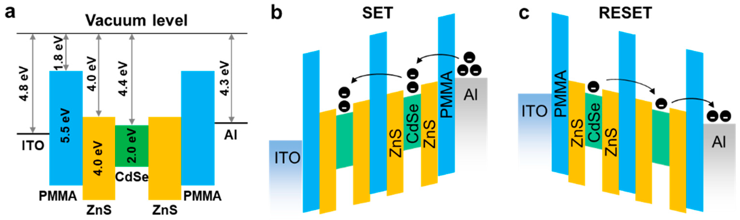
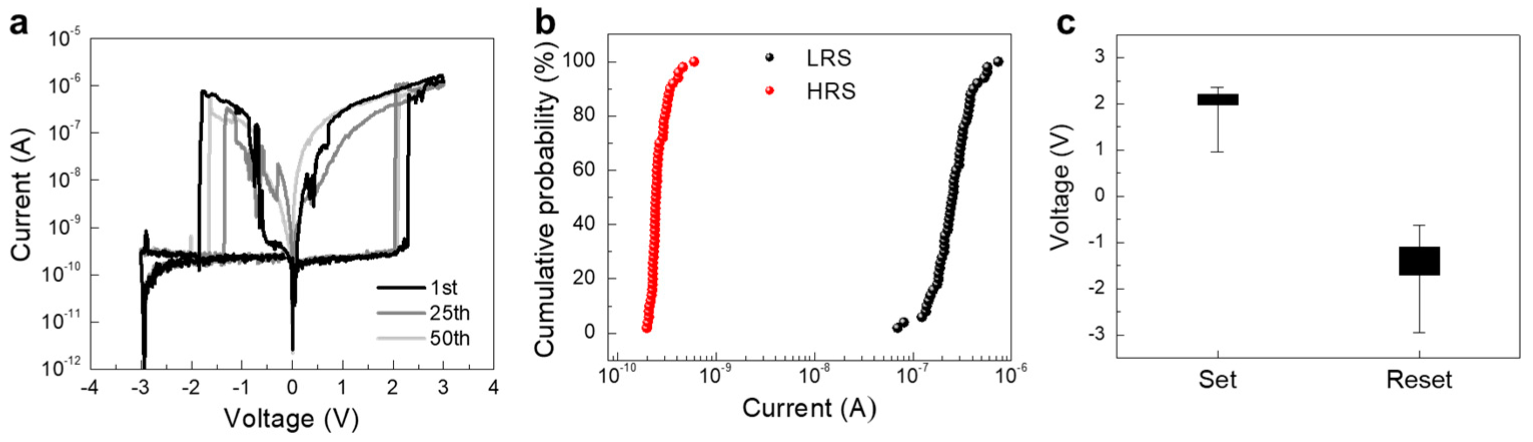
3.1. Device Structure and Electrical Characteristics

Figure 1a shows the device structure of the CdSe/ZnS QD-PMMA memristor device. The device has an asymmetric electrode structure with a high work-function ITO (Φ ~ 4.8 eV) used as a bottom electrode and a low work-function Al (Φ ~ 4.3 eV) used as a top electrode [24]. The CdSe/ZnS QD-PMMA layer, which is positioned between the ITO and Al electrodes, had an average thickness of 204.8 nm. As shown in Figure 1b, the CdSe/ZnS QDs were well dispersed in the PMMA matrix without noticeable agglomeration of the QD particles (QD concentration: 1 wt%). Figure 1c shows the light absorbance and normalized PL spectra of the CdSe/ZnS QDs, which were measured in the toluene solution. The CdSe/ZnS QDs showed an emission peak centered at around 530 nm, which corresponds to a bandgap of ~2.34 eV. Additionally, the full-width-half-maximum of the PL peak was ~34.5 nm, showing a narrow distribution of the QD size.
In the QD-polymer based memristors, electron trapping and de-trapping occurring at the QDs play the dominant role, affecting memory characteristics such as the set/reset voltages, memory margin, and the current switching ratio [25]. In particular, the large band offset between the polymer and the QDs allows effective electron trapping at the QDs. Since the charge trapping characteristics are mainly governed by the embedded CdSe/ZnS QDs, it is necessary to optimize the CdSe/ZnS QD concentration in the polymer matrix. To optimize the QD concentration, we varied the concentration of CdSe/ZnS QDs as 1, 3, and 5 wt%, which correspond to volume concentrations of 0.21, 0.63, and 1.05 v/v%, respectively. Typical I-V characteristics of CdSe/ZnS QD-PMMA memristor devices are shown in Figure 1d when the CdSe/ZnS QD concentration was 1 and 3 wt%. Clearly, in both devices, set and reset operations accompanying abrupt changes of resistance states were observed. Initially, upon sweeping the bias to the positive bias direction, the device was in a high-resistance state (HRS). Then, at around 2.5 to 3 V, a transition to a low-resistance state (LRS) was observed, which is regarded as the set process. Particularly, at around the set bias, the current variation was approximately ~104 and 102~103 for 1 wt% and 3 wt% devices, respectively, which are comparable to those of TiO2-based memristors [26]. The LRS maintained after the set process until a sufficient negative bias was applied (~−2 V); then, a transition from LRS to HRS was induced. Increasing the CdSe/ZnS QD concentration to 5 wt%, however, resulted in abnormal I-V behavior showing mostly either insulating or conducting characteristics. In particular, as shown in Figure 1e, the device with conducting behavior followed the Ohmic conduction mechanism (linear I-V) with a relatively large current level (>10−2 A), while the device with insulating behavior exhibited relatively low current levels (<10−7 A). Since the PMMA is an insulating polymer and only a weak electric field is applied to the device during the operation (<0.20 MV/cm), it is likely that the occurrence of conducting or insulating characteristics is due to the agglomeration of CdSe/ZnS QDs in PMMA. For instance, when the number of QD particles is low at a specific region, the device could operate similar to a metal-insulator-metal diode exhibiting insulating behavior. On the other hand, when the QDs are agglomerated in a restricted region, specific conductive pathways could be formed [27], resulting in a highly conducting state.

3.2. Operation Mechanism of CdSe/ZnS QD-PMMA Memristors

Concerning the set and reset processes, the operating mechanism can be described as follows. As shown in Figure 2a, due to the large difference between the lowest-unoccupied-molecular-orbital (LUMO) level of PMMA and the work function of Al, the PMMA is likely to act as a charge blocking layer. Additionally, the difference between the highest-occupied-molecular-orbital level of PMMA and the work function of ITO is large enough (ΔE~2.5 eV) to effectively block the hole injection from the ITO electrode. When a positive bias is applied to the ITO electrode, electrons start to inject from the Al electrode into the CdSe/ZnS QD-PMMA layer and trapped at the CdSe/ZnS QDs (Figure 2b). Here, due to the large difference between the LUMO level of PMMA and the conduction band minimum of CdSe/ZnS QDs (2.2 to 2.6 eV) [28], it is likely that the trapped electrons are well-confined in the QDs. Then, when a sufficiently high bias is applied, the electric field formed between the QDs is increased, and consequently, the electronic occupation probability of the QDs increases [25], leading to a shift of Fermi level toward the LUMO level of PMMA [25]. This, in fact, may generate conducting filaments in the CdSe/ZnS QD-PMMA layer, resulting in the LRS [29]. On the other hand, when a negative bias is applied to the ITO electrode, electrons are de-trapped from the CdSe/ZnS QDs and the device returns to the initial HRS, as shown in Figure 2c.
Obtaining uniform and stable switching characteristics is a prerequisite for realizing highly reliable memristor devices. To evaluate the operational stability of the CdSe/ZnS QD-PMMA memristors, the I-V characteristics were measured repeatedly for 50 times and the variation of the switching behavior was analyzed. Figure 3a shows the I-V curves obtained at the 1st, 25th, and 50th measurements. As displayed, the device exhibited stable switching characteristics during the repetitive operation with the current switching ratio in the range of 103~104. Figure 3b,c show the corresponding cumulative distribution of currents at LRS and HRS, and the variation of set/reset voltages, respectively. Particularly, the current at the LRS was in the range of 2.0~6.0 × 10⁻¹⁰ A, and at HRS, the current was in the range of 0.7~7.3 × 10⁻⁷ A. Additionally, the set and reset voltages were varied in the ranges of 2.09 ± 0.159 V and −1.26 ± 0.307 V, respectively. Nonetheless, these results show that the CdSe/ZnS QD-PMMA memristors exhibit relatively stable switching characteristics.

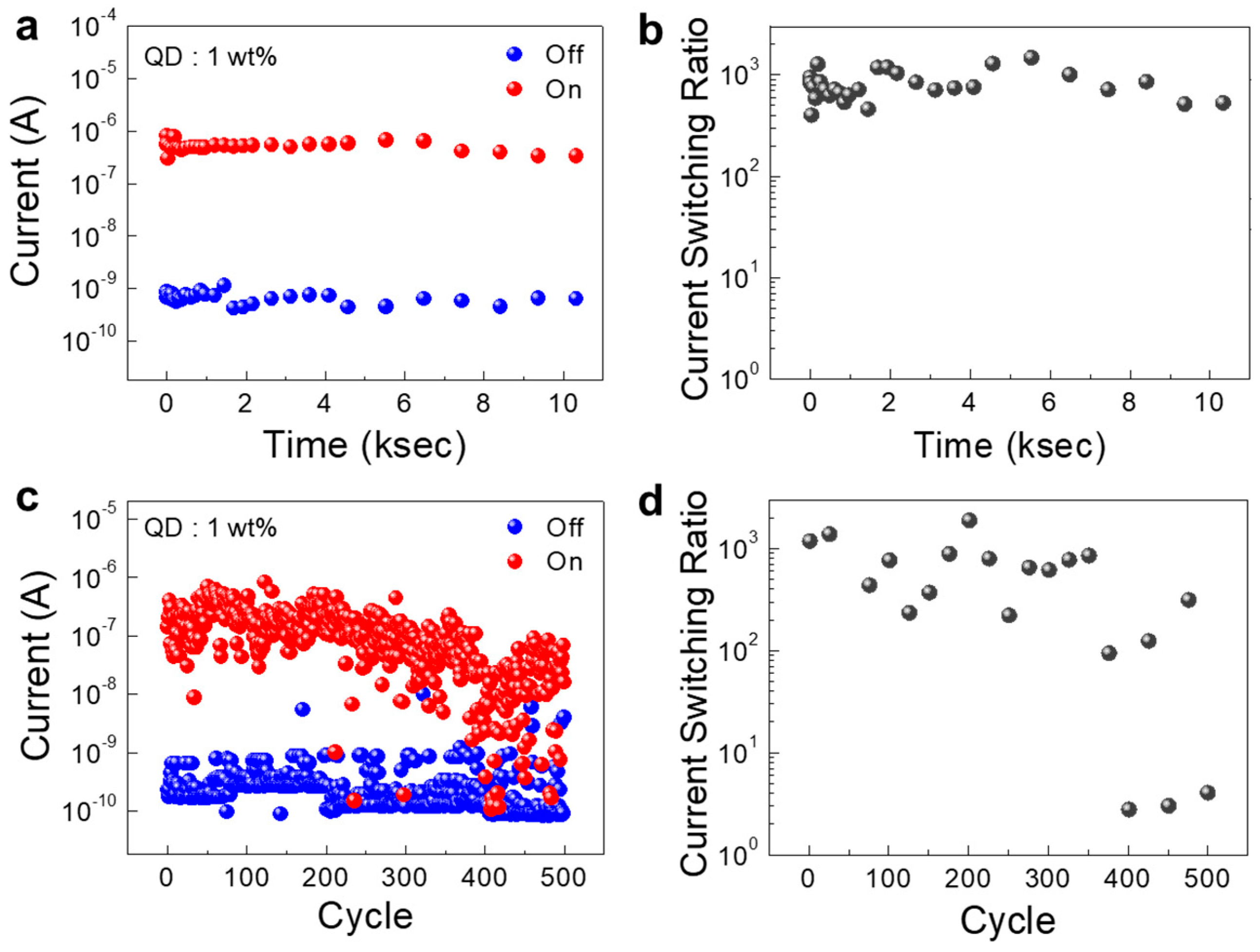
3.3. Operation Stability of CdSe/ZnS QD-PMMA Memristors

To further demonstrate the stable switching oepration of CdSe/ZnS QD-PMMA memristors, the data retention and the endurance characteristics were analyzed. Particularly, the data retention and the endurance characteristics are important for memristor devices because they reflect the reliability of memory functions. Additionally, since the switching between the LRS and HRS relies on the trapping and de-trapping of electrons at the CdSe/ZnS QDs, it is important to determine any undesired degradation of the device which may result in a loss of memory state. To evaluate the data retention characteristics of CdSe/ZnS QD-PMMA memristors, the device was programmed to either the LRS or HRS state using a Vbias of +3 V or −3 V, respectively, and the variation of the current level was traced with Vread of +1 V. Here, Vread was set to +1 V, which is lower than the typical set bias. Figure 4a shows the time-dependent current variation for LRS and HRS states up to ~10 ks. As displayed, the LRS and HRS states were well-maintained without a significant change in the current level. The corresponding current switching ratio variation is shown in Figure 4b, and up to ~10 ks, the switching ratio was maintained at around 103. These results indicate that the electrons trapped at the CdSe/ZnS QDs are energetically stable and the de-trapping and/or recombination of electrons rarely occurred during this period. Figure 4c shows the endurance measurement data in which the set and reset operations were repeatedly performed for up to 500 cycles. Here, the Vset and Vreset were +3 V and −3 V, respectively, and each Vset or Vreset was applied for 50 ms (Vread = +1 V). As shown in Figure 4c, the device exhibited relatively stable switching between LRS and HRS with the current switching ratio maintaining at ~103 (Figure 4d). We observed, however, that after around 400 cycles of set/reset switching, the device started to show occasional unstable operation with reduced switching ratios. This can be more clearly identified in Figure 4d, where the variation of the current switching ratio is displayed as a function of the cycle number. These results imply that the device may experience particial degradation, possibly owing to the change in the conduction mechanism.

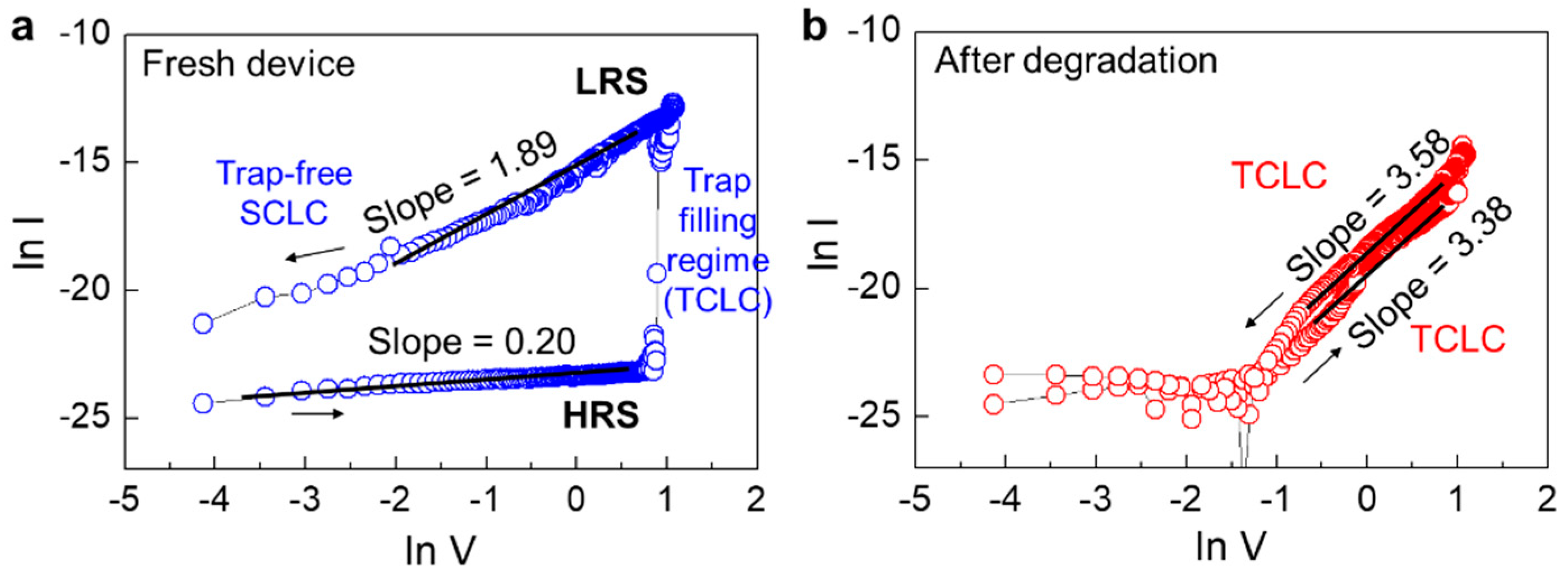
3.4. Degradation Mechanisms

To closely investigate the possible origin for the instability occurring at high-number cycles, the conduction mechanism change during the switching operation was analyzed in detail. Figure 5a,b show the ln I vs. ln V plots for the CdSe/ZnS QD-PMMA memristor before (fresh device) and after the degradation (device underwent 500 endurance cycles), respectively. The fresh device showed a clear difference in the conduction mechanism at HRS and LRS regions. Initially in the HRS region, the I-V curve followed I ∝ V0.2. Then, at around the set voltage (+2.3 V), the slope (α) becomes larger than 2, indicating a transition to the trap filling regime or the TCLC [30]. The presence of the TCLC regime is an indication that the traps are exponentially distributed in the forbidden gap [30], and at this stage, the injected electrons fill the trap levels. Followingly, after the set process, the dominant conduction mechanism changes to trap-free SCLC, showing the relation, I ∝ V1.89. Ideally, for the trap-free SCLC, the I-V is related by the following equation [17,31].
I 9 ε i μ V 2 8 d 3
where εi is the insulator permittivity, μ is the carrier mobility and d is the insulator thickness. As displayed in Figure 5a, the α value in the LRS region (1.89) is similar to that of the ideal case, suggesting that most of the traps are filled with the electrons during the set process. These transitions in conduction mechanism are in a good agreement with the operation mechanism described in Figure 2. After the degradation, however, the dominant conduction mechanisms and their transitions are significantly different from the fresh device. Figure 5b shows the ln I vs. ln V plot, which is measured after the degradation. Interestingly, the I-V characteristics were similar in both forward and reverse sweeps. For the forward and reverse sweeps, the corresponding α values were 3.38 and 3.58, respectively. Thus, the dominant conduction mechanism is considered as the TCLC, suggesting that during the repeated operation, additional traps are created in the CdSe/ZnS QD-PMMA layer, preventing the occurrence of trap-free SCLC behavior. Previously, it has been reported that electronic trap states can be created and eliminated in the CdSe CQDs [31]. Particularly, by doping and charging, atomic dimmers at the QD surface can be formed or broken, creating trap states within the bandgap [32]. Moreover, the oxidation of reactive metallic components in QD particles can be another possible reason for the creation of additional trap states. Nevertheless, from our observation, it is clear that the dominant conduction mechanism is changed after the degradation, possibly originating from the creation of additional trap states in the CdSe/ZnS QD-PMMA layer. Therefore, to obtain highly reliable QD-polymer-based memristors, surface-stabilized QDs and the prevention of oxidative reactions would be necessary.

4. Conclusions

In this paper, we demonstrated solution-processed CdSe/ZnS QD-PMMA-based memristors for potential memory and neuromorphic applications. The fabricated memristors exhibited a high retention time over 104 s and good stability, having an endurance cycle up to 400 times. Additionally, to understand the degradation mechanism, we investigated the conduction mechanism change before and after the degradation. It was determined that the dominant conduction mechanism changed from the trap-free SCLC mechanism to TCLC, suggesting that additional trap states are generated in the CdSe/ZnS QD-PMMA layer during the repeated operation, causing a permanent failure of the device.

Author Contributions

Conceptualization, M.K., J.K. and Y.-H.K.; methodology, M.K., S.O., J.K. and Y.-H.K.; formal analysis, M.K., S.O. and S.S.; investigation, M.K. and S.O.; resources, J.K. and Y.-H.K.; data curation, M.K., J.K. and Y.-H.K.; writing—original draft preparation, M.K., S.O., J.K. and Y.-H.K.; writing—review and editing, J.K. and Y.-H.K.; visualization, M.K. and S.O.; funding acquisition, J.K. and Y.-H.K. All authors have read and agreed to the published version of the manuscript.

Funding

This study was supported by the National Research Foundation (NRF) of Korea, grant funded by the Korea Government (Ministry of Science and ICT; NRF-2017R1E1A1A01077189 and NRF-2019M3F3A1A02071601) and by the Ministry of Trade, Industry and Energy and Korea Institute for Advancement of Technology through the International Cooperative R&D program (P0011268).

Institutional Review Board Statement

Not applicable.

Informed Consent Statement

Not applicable.

Conflicts of Interest

The authors declare no conflict of interest.

References

  1. Jeong, D.S.; Kim, I.; Ziegler, M.; Kohlstedt, H. Towards artificial neurons and synapses: A materials point of view. RSC Adv. 2013, 3, 3169–3183. [Google Scholar] [CrossRef]
  2. Hu, S.G.; Liu, Y.; Liu, Z.; Chen, T.P.; Wang, J.J.; Yu, Q.; Deng, L.J.; Yin, Y.; Hosaka, S. Associative memory realized by a reconfigurable memristive Hopfield neural network. Nat. Commun. 2015, 6, 7522. [Google Scholar] [CrossRef] [Green Version]
  3. Pi, S.; Li, C.; Jiang, H.; Xia, W.; Xin, H.; Yang, J.J.; Xia, Q. Memristor crossbar arrays with 6-nm half-pitch and 2-nm critical dimension. Nat. Nanotechnol. 2019, 14, 35–39. [Google Scholar] [CrossRef] [PubMed]
  4. Ielmini, D.; Wong, H.S.P. In-memory computing with resistive switching devices. Nat. Electron. 2018, 1, 333–343. [Google Scholar] [CrossRef]
  5. Sheng, X.; Graves, C.E.; Kumar, S.; Li, X.; Buchanan, B.; Zheng, L.; Lam, S.; Li, C.; Strachan, J.P. Low-Conductance and Multilevel CMOS-Integrated Nanoscale Oxide Memristors. Adv. Electron. Mater. 2019, 5, 1800876. [Google Scholar] [CrossRef]
  6. Jang, B.C.; Nam, Y.; Koo, B.J.; Choi, J.; Im, S.G.; Park, S.-H.K.; Choi, S.-Y. Memristive Logic-in-Memory Integrated Circuits for Energy-Efficient Flexible Electronics. Adv. Funct. Mater. 2018, 28, 1704725. [Google Scholar] [CrossRef]
  7. Lipatov, A.; Li, T.; Vorobeva, N.S.; Sinitskii, A.; Gruverman, A. Nanodomain Engineering for Programmable Ferroelectric Devices. Nano Lett. 2019, 19, 3194–3198. [Google Scholar] [CrossRef]
  8. Krestinskaya, O.; Ibrayev, T.; James, A.P. Hierarchical Temporal Memory Features with Memristor Logic Circuits for Pattern Recognition. IEEE TCAD 2018, 37, 1143–1156. [Google Scholar] [CrossRef]
  9. Wang, Z.; Joshi, S.; Savel’ev, S.E.; Jiang, H.; Midya, R.; Lin, P.; Hu, M.; Ge, N.; Strachan, J.P.; Li, Z.; et al. Memristors with diffusive dynamics as synaptic emulators for neuromorphic computing. Nat. Mater. 2017, 16, 101–108. [Google Scholar] [CrossRef] [Green Version]
  10. Lanza, M.; Wong, H.-S.P.; Pop, E.; Ielmini, D.; Strukov, D.; Regan, B.C.; Larcher, L.; Villena, M.A.; Yang, J.J.; Goux, L.; et al. Recommended methods to study resistive switching devices. Adv. Elect. Mater. 2019, 5, 1800143. [Google Scholar] [CrossRef] [Green Version]
  11. Strukov, D.B.; Snider, G.S.; Stewart, D.R.; Williams, R.S. The missing memristor found. Nature 2008, 453, 80–83. [Google Scholar] [CrossRef] [PubMed]
  12. Sharma, P.; Zhang, Q.; Sando, D.; Lei, C.H.; Liu, Y.; Li, J.; Nagarajan, V.; Seidel, J. Nonvolatile ferroelectric domain wall memory. Sci. Adv. 2017, 3, e1700512. [Google Scholar] [CrossRef] [PubMed] [Green Version]
  13. Kent, A.D.; Worledge, D.C. A new spin on magnetic memories. Nat. Nanotechnol. 2015, 10, 187–191. [Google Scholar] [CrossRef]
  14. Wuttig, M.; Bhaskaran, H.; Taubner, T. Phase-change materials for non-volatile photonic applications. Nat. Photonics 2017, 11, 465–476. [Google Scholar] [CrossRef]
  15. Wu, C.; Kim, T.W.; Choi, H.Y.; Strukov, D.B.; Yang, J.J. Flexible three-dimensional artificial synapse networks with correlated learning and trainable memory capability. Nat. Commun. 2017, 8, 752. [Google Scholar] [CrossRef] [PubMed] [Green Version]
  16. van de Burgt, Y.; Melianas, A.; Keene, S.T.; Malliaras, G.; Salleo, A. Organic electronics for neuromorphic computing. Nat. Electron. 2018, 1, 386–397. [Google Scholar] [CrossRef]
  17. Son, D.I.; Kim, T.W.; Shim, J.H.; Jung, J.H.; Lee, D.U.; Lee, J.M.; Park, W.I.; Choi, W.K. Flexible Organic Bistable Devices Based on Graphene Embedded in an Insulating Poly(methyl methacrylate) Polymer Layer. Nano Lett. 2010, 10, 2441–2447. [Google Scholar] [CrossRef]
  18. Sun, Y.; Wen, D.; Bai, X.; Lu, J.; Ai, C. Ternary Resistance Switching Memory Behavior Based on Graphene Oxide Embedded in a Polystyrene Polymer Layer. Sci. Rep. 2017, 7, 3938. [Google Scholar] [CrossRef]
  19. Li, X.; Zhao, Y.-B.; Fan, F.; Levina, L.; Liu, M.; Quintero-Bermudez, R.; Gong, X.; Quan, L.N.; Fan, J.; Yang, Z.; et al. Bright colloidal quantum dot light-emitting diodes enabled by efficient chlorination. Nat. Photonics 2018, 12, 159–164. [Google Scholar] [CrossRef]
  20. Ma, Z.; Ooi, P.C.; Li, F.; Yun, D.Y.; Kim, T.W. Electrical Bistabilities and Conduction Mechanisms of Nonvolatile Memories Based on a Polymethylsilsesquioxane Insulating Layer Containing CdSe/ZnS Quantum Dots. J. Electron. Mater. 2015, 44, 3962–3966. [Google Scholar] [CrossRef]
  21. Nayak, D.; Choudhary, R.B. Augmented optical and electrical properties of PMMA-ZnS nanocomposites as emissive layer for OLED applications. Opt. Mater. 2019, 91, 470–481. [Google Scholar] [CrossRef]
  22. Koo, B.M.; Sung, S.; Wu, C.; Song, J.-W.; Kim, T.W. Flexible organic synaptic device based on poly (methyl methacrylate):CdSe/CdZnS quantum-dot nanocomposites. Sci. Rep. 2019, 9, 9755. [Google Scholar] [CrossRef]
  23. Zhou, Z.; Mao, H.; Wang, X.; Sun, T.; Chang, Q.; Chen, Y.; Xiu, F.; Liu, Z.; Liu, J.; Huang, W. Transient and flexible polymer memristors utilizing full-solution processed polymer nanocomposites. Nanoscale 2018, 10, 14824–14829. [Google Scholar] [CrossRef]
  24. Son, D.-I.; Park, D.-H.; Ie, S.-Y.; Choi, W.-K.; Choi, J.-W.; Li, F.; Kim, T.-W. Single active-layer structured dual-function devices using hybrid polymer–quantum dots. Nanotechnology 2008, 19, 395201. [Google Scholar] [CrossRef] [PubMed]
  25. Kim, D.H.; Wu, C.; Park, D.H.; Kim, W.K.; Seo, H.W.; Kim, S.W.; Kim, T.W. Flexible Memristive Devices Based on InP/ZnSe/ZnS Core–Multishell Quantum Dot Nanocomposites. ACS Appl. Mater. Interfaces 2018, 10, 14843–14849. [Google Scholar] [CrossRef] [PubMed]
  26. Alibart, F.; Zamanidoost, E.; Strukov, D.B. Pattern classification by memristive crossbar circuits using ex situ and in situ training. Nat. Commun. 2013, 4, 2072. [Google Scholar] [CrossRef] [PubMed] [Green Version]
  27. Kim, D.H.; Kim, W.K.; Woo, S.J.; Wu, C.; Kim, T.W. Highly-reproducible nonvolatile memristive devices based on polyvinylpyrrolidone: Graphene quantum-dot nanocomposites. Org. Electron. 2017, 51, 156–161. [Google Scholar] [CrossRef]
  28. Shim, J.H.; Jung, J.H.; Lee, M.H.; Kim, T.W.; Son, D.I.; Han, A.N.; Kim, S.W. Memory mechanisms of nonvolatile organic bistable devices based on colloidal CuInS2/ZnS core–shell quantum dot—Poly(N-vinylcarbazole) nanocomposites. Org. Electron. 2011, 12, 1566–1570. [Google Scholar] [CrossRef]
  29. Ko, S.H.; Yoo, C.H.; Kim, T.W. Electrical Bistabilities and Memory Stabilities of Organic Bistable Devices Utilizing C60Molecules Embedded in a Polymethyl Methacylate Matrix with an Al2O3 Blocking Layer. J. Electrochem. Soc. 2012, 159, G93–G96. [Google Scholar] [CrossRef]
  30. Son, D.I.; Park, D.H.; Choi, W.K.; Cho, S.H.; Kim, W.T.; Kim, T.W. Carrier transport in flexible organic bistable devices of ZnO nanoparticles embedded in an insulating poly(methyl methacrylate) polymer layer. Nanotechnology 2009, 20, 195203. [Google Scholar] [CrossRef]
  31. Ling, Q.-D.; Liaw, D.-J.; Zhu, C.; Chan, D.S.-H.; Kang, E.-T.; Neoh, K.-G. Polymer electronic memories: Materials, devices and mechanisms. Prog. Polym. Sci. 2008, 33, 917–978. [Google Scholar] [CrossRef]
  32. Voznyy, O.; Thon, S.M.; Ip, A.H.; Sargent, E.H. Dynamic Trap Formation and Elimination in Colloidal Quantum Dots. J. Phys. Chem. Lett. 2013, 4, 987–992. [Google Scholar] [CrossRef] [PubMed]
Figure 1. (a) Device structure and an optical image of solution-processed CdSe/ZnS QD-PMMA memristors. (b) Cross-sectional TEM images of the CdSe/ZnS QD-PMMA memristor. The inset shows the structure of CdSe/ZnS QDs with oleic acid as the ligand. (c) Light absorption and photoluminescence (PL) characteristics of CdSe/ZnS QDs. (d) Current-voltage (I-V) characteristics of CdSe/ZnS QD-PMMA memristors with QD concentrations of 1 wt% and 3 wt%, and (e) 5 wt%.
Applsci 11 05020 g001
Figure 2. (a) An energy band diagram of the CdSe/ZnS QD-PMMA memristor. The change in the energy band diagram of the device during (b) set, and (c) reset process.
Applsci 11 05020 g002
Figure 3. (a) I-V characteristics of CdSe/ZnS QD-PMMA memristors during a cyclic test (50 cycles) (QD: 1 wt%). (b) The variation of LRS and HRS currents during the cyclic test. (c) The distribution of set and reset voltages during the cyclic test.
Applsci 11 05020 g003
Figure 4. (a) The data retention characteristics of the CdSe/ZnS QD-PMMA memristor (QD: 1wt%). The LRS and HRS states were programmed with biases of +3 V and −3 V, respectively. Additiaonally, the Vread was +1 V. (b) The variation of current switching ratio during the data retention test up to 104 s. (c) The endurance cyclic test data of the CdSe/ZnS QD-PMMA memristor (500 cycles). The LRS and HRS states were programmed with biases of +3 V and −3 V, respectively. Additionally, the Vread was +1 V. (d) The variation of current switching ratio during the endurance test.
Applsci 11 05020 g004
Figure 5. (a) Current-voltage (I-V) curves of the CdSe/ZnS QD-PMMA memristor, (a) fresh device, and (b) after degradation.
Applsci 11 05020 g005
Publisher’s Note: MDPI stays neutral with regard to jurisdictional claims in published maps and institutional affiliations.

