Abstract
The degradation effect of a field-programmable gate array becomes a significant issue due to the high density of logic circuits inside the field-programmable gate array. The degradation effect occurs because of the rapid technology scaling process of the field-programmable gate array while sustaining its performance. One parameter that causes the degradation effect is the delay occurrence caused by the hot carrier injection and negative bias temperature instability. As such, this research proposed a multipoint detection technique that detects the delay occurrence caused by the hot carrier injection and negative bias temperature instability degradation effects. The multipoint detection technique also assisted in signaling the aging effect on the field-programmable gate array caused by the delay occurrence. The multipoint detection technique was also integrated with a method to optimize the performance of the field-programmable gate array via an automatic clock correction scheme, which could provide the best clock signal for prolonging the field-programmable gate array performance that degraded due to the degradation effect. The delay degradation effect ranged from 0° to 360° phase shifts that happened in the field-programmable gate array as an input feeder into the multipoint detection technique. With the ability to provide closed-loop feedback, the proposed multipoint detection technique offered the best clock signal to prolong the field-programmable gate array performance. The results obtained using the multipoint detection technique could detect the remaining lifetime of the field-programmable gate array and propose the best possible signal to prolong the field-programmable gate array’s performance. The validation showed that the multipoint detection technique could prolong the performance of the degraded field-programmable gate array by 13.89%. With the improvement shown using the multipoint detection technique, it was shown that compensating for the degradation effect of the field-programmable gate array with the best clock signal prolonged the performances.
1. Introduction
Field-programmable gate arrays (FPGAs) are eminently utilized to develop the latest complementary metal oxide semiconductor (CMOS) technology due to their high volume density, scalability, and ability to cope with the highest performance demands for digital and mixed-mode analog applications. However, after the rapid downscaling in FPGAs, the device encounters challenges, including increased noise sensitivity, manufacturing variability, and reliability concerns [1,2,3,4]. These factors escalate the degradation of the chip performance, which eventually reduces the lifespan of the product. Numerous reports elaborate on delays that occur in FPGAs, which are detrimental to chip performance [5,6,7,8,9,10]. The optimization of delays has been studied by using key testing parameters, such as lookup tables (LUTs) and algorithm analysis [11,12]. L. Bauer et al. studied the dependency of application types with fault delay [13]. The prediction of interconnect delays was studied by V. Manohararajah et al. [14]. It was deduced that the timing model is beneficial for the physical synthesis flow of an FPGA design [15,16].
It has been reported that the delay is the effect of a negative bias temperature instability (NBTI), which is a critical factor of FPGA degradation [17,18,19]. S. Chakravarthi et al. [20] developed a framework that caused a delay of less than 500 ms. Previous studies primarily concentrated on the NOR gate chains, which are found to reduce delay degradation [21]. The effects of delay on switching activity were discovered by D. Alnajjar et al. [22], who reported on the analysis of the reduction of the circuit speed. Meanwhile, M. Cho et al. [23] believed that the delay component is a temperature-activated process in irradiated devices. S. Cha et al. [24] observed that the delay is caused by an increase in the current and subsequent redistribution of the voltage. The nominal delay degradation for the ISCAS Benchmark indicates that the delay degradation in semiconductor devices can be as low as 617 ps [25].
Seven output ranges of a phase-detection aging sensor with a lifetime prediction table for different FPGAs manufacturers are proposed to guide system designers and industrial players through simulation and experimental validation. After that, an automatic clock correction method was proposed and validated through experiments to stabilize the system’s performance with the best clock signal for the entire FPGA system to counter the aging degradation and maintain the system’s performance.
This paper is organized as follows. First, Section 2 describes the lifetime reliability sensing in FPGAs and Section 3 describes the methodology of analyzing aging sensors with multiple point detection. Then, Section 4 compares multiple types of delay frequencies, which was validated through the experimental work presented in Section 5. Finally, the conclusion is presented in Section 6.
2. Lifetime Reliability Sensing in FPGAs
One of the first effective aging sensors developed was that proposed by C. Leong et al. [26], which detects delays in circuits. However, the method is unable to characterize the delay using different amounts of phase delay. Meanwhile, the aging sensors that were proposed by A. Amouri et al. [27] place the aging sensor in a critical path to avoid late transitions occurring in the circuit. The aging sensor [28,29] and FPGA chips were reprogrammed to reduce the late transition effects caused by NBTI [30] and hot carrier injection (HCI). Meanwhile, M. Valdes-Pena proposed an aging sensor without determining a specific delay range [31]. Due to the limitations listed above, an enhanced aging detection system for particular ranges of phase delays is needed to effectively detect aging in FPGAs. This work proposed a lifetime prediction method such that it implements multiple phase detection.
The FPGA lifetime prediction technique proposed in this work uses the aging sensor detection circuit, which implements the multiple-phase delay capability using a clock generator. The method employs a sensor detector with seven phase delay ranges, consequently estimating the delay occurring in the chip. This information is eventually used to obtain the remaining lifetime of the FPGA while operating with a critical level indicator for replacement.
Lifetime Reliability at the Transistor Level
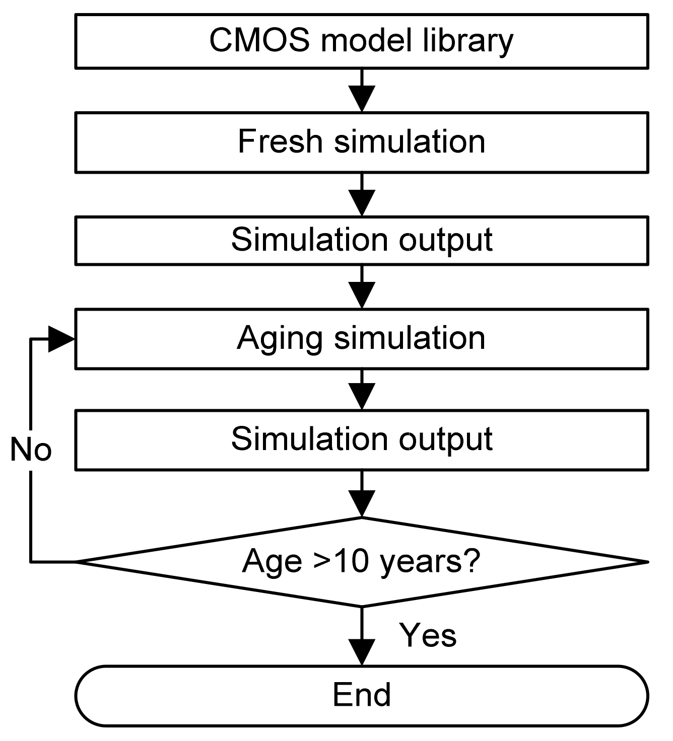
M. Ebrahimi et al. discovered the importance of lifetime reliability at the transistor level [32]. The importance of lifetime reliability was supported by G. Sai et al., who found that aging sensor detection is caused by multiple path delays generated at the transistor level [33]. The Eldo simulator tool was used in this work to predict the lifetime reliability in a 23-stage ring oscillator [34,35,36]. The simulation flow using the Eldo simulator is shown in Figure 1. The 45 nm high-power model for positive metal oxide semiconductor (PMOS) and negative metal oxide semiconductor (NMOS) transistors from the predictive technology model (PTM) [37] was used in the 23-stage ring oscillator. The ring oscillator circuit was simulated as a new circuit without an aging property to obtain the oscillation frequency. The new simulation was conducted as a reference point for the zero-degradation effect. The behavioral characteristics of the ring oscillator circuit were verified through the simulation output. The Eldo simulator then employed an advanced reliability model, which took the HCI and NBTI of CMOS devices into account in order to simulate 10 years of aging effects in the circuit. These aging simulations were conducted for the first year until ten years of aging circuit to determine the trend of the device degradation. The models used in this work were based on reaction–diffusion theory [38] and were multimode energy driven [39].
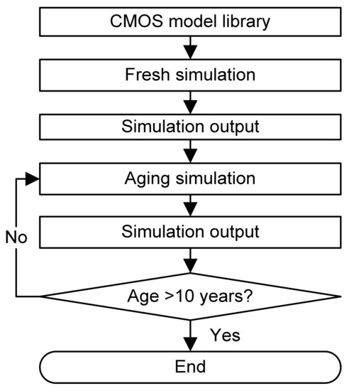
Figure 1.
Simulation flow of the Eldo simulator for fresh and aging devices.
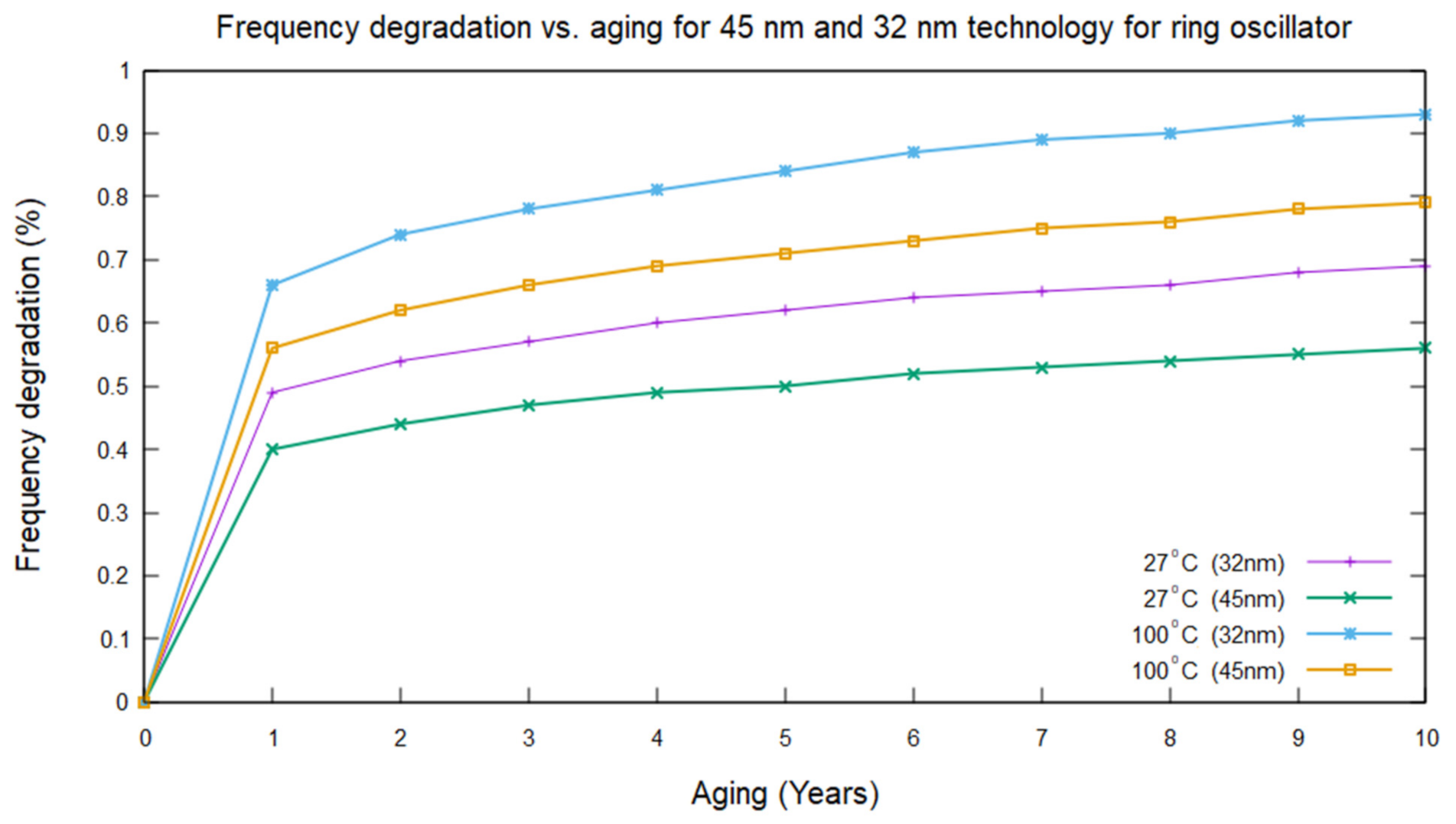
Figure 2 shows the frequency degradations for 45 nm and 32 nm technologies on a ring oscillator for 27 °C and 100 °C for up to 10 years of aging, which were obtained from the Eldo simulator. This frequency degradation shows that the frequency increased after aging due to the HCI and NBTI mechanisms at 27 °C and 100 °C, respectively [40]. Yoohwan Kim et al. found that the NBTI effect is a dominant factor when the temperature is high, and the effect can be suppressed for lower temperatures [41,42]. Hui Zhang et al. reported that under stressed conditions of PMOS transistor exposed to a gate voltage of 0 V to 2.5 V and a high temperature of 100 °C, new interface states of Si–SiO2 cause electric potential augmentation [40]. Furthermore, the threshold voltage causes a negative drift because of fixed charge and interface states caused by a positive hole capture. A reaction–diffusion model was well explained by Wenping Wang [43], including the principle of the NBTI effect, which reported the breaking of the Si–H bond in the Si–SiO2 interface into interface traps [44,45]. It was shown that these findings support this work due to frequency variations that were caused by the HCI and NBTI degradations.
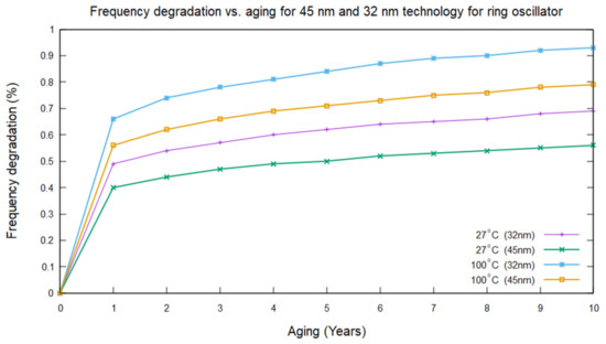
Figure 2.
Frequency degradation versus aging for 45 nm and 32 nm technology ring oscillators at 27 °C and 100 °C caused by HCI and NBTI, respectively.
D. Sengupta and S. Sapatnekar obtained a threshold voltage shift due to NBTI [46] as given in Equation (1):
where is a constant that depends on the process, voltage, and temperature (PVT); is the effective stress time after the elapsed time between and The effective stress time for PMOS devices after NBTI stress with a LOW input signal depends on the stress probability value of the device. Therefore, Equation (2) was obtained using CurveExpert® (Chattanooga, TN, USA) [47] software to calculate the degradation caused by NBTI for a high temperature of 100 °C for a 45 nm technology node:
Equation (2) can be used to calculate an unknown frequency degradation that is not plotted in Figure 2. As was deduced from Equation (2), the percentage of frequency degradation against new devices for 5 years and 6 months was equal to 0.723% frequency degradation due to the NBTI effect.
The HCI degradation mechanism is more influential in NMOS than PMOS transistors [48]. HCI occurs when carriers inside the channel are subjected to the adjacent electric field, producing sufficient energy and momentum to break the barriers surrounding the dielectric [46]. The carriers with adequate energy for the HCI stress will result in interface-state generation at the Si–SiO2 interface [49]. Furthermore, D. Sengupta and S. Sapatnekar produced an equation of the threshold voltage degradation due to the HCI [46], as given in Equation (3):
where and are the process dependent parameters, is a vertical field, q is the electronic charge, is the trap generation energy, is the hot electron mean free path, is the lateral electrical field, and g is effective stressing time. The adequate stressing time caused by HCI aging depends on the number of switching events of the transistor. It can be calculated using where AF is the activity factor of the transistor, is the clock frequency, and t is the elapsed time. Therefore, D. Sengupta and S. Sapatnekar combined the degradation effect of the NBTI and HCI onto a shift in delay for logic gates in detail [46], as stated in Equation (4):
where and . By using the CurveExpert® (Chattanooga, TN, USA) [47] software, the frequency degradation due to the HCI at 27 °C could be calculated using Equation (5) for a 45 nm technology node:
As was deduced from Equation (5), the frequency degradation caused by the HCI for 8 years and 3 months was equal to 0.542% frequency degradation compared to new devices.
In summary, the results indicate that the HCI and NBTI mainly caused the degradation effect, which is supported by C.Q. Liu et al.’s study, which reveals that the delay degradation effect due to the HCI and NBTI led to device aging [50]. However, most studies in the open literature have not explicitly examined the 45 nm technology node. Therefore, this simulation work using the Eldo simulator mainly focused on reliability concerns due to the HCI and NBTI degradation effect of a 23-stage ring oscillator for a 45 nm technology node.
3. The Design Process for an Aging Sensor with Multiple Points of Frequency Detection
Figure 3 presents the proposed flow of aging sensor detection. The aging sensor detector has two main inputs, which are the clock (Clk) and voltage (Vi); the clock skew effect is negligible [51,52]. This detection circuit will produce seven ranges of phase point detection ranging from 0°/360° to 300° with a 50° resolution. Phase point detection is a technique that segregates the detection process of the delay signal into several types of frequency detections. Each detection process ranging from 0 to 49° represents level 0, while the phase detection range of 50–99° represents level 50, and so forth. The total delay time for level 0 was from 0 s to 1.39 ns, and level 50 was from 1.39 ns to 2.78 ns. Therefore, the detection process was applicable only if the frequency of Vi was less than the frequency of the Clk such that it produced a successful detection.

Figure 3.
The schematic diagram for an aging sensor detector.
The Clk was synchronized to the clock of the FPGA circuit using a clock generator that provided a stable clock for the entire system. The input signal originated from an external clock, and the output produced was a synchronous clock called clk_cntrl, which triggered the Clock Delay and circuit under test (CUT) modules. The Clk may originate from the various FPGA manufacturers with different intellectual properties (IPs). The Xilinx FPGA used in this work has a reset input and locked outputs that are used for initialization purposes. There is also an indicator called a clocking wizard (CW) signal that is fully stable. The Xilinx FPGA board provides an IP that requires 69 clock cycles to stabilize the clock. For the proposed aging sensor circuit, the programmer requires the CW to conduct a frequency synthesis and phase alignment to manipulate the frequency and duty cycles of the synchronized clock. Based on this CW specification, two clock inputs served as the primary and secondary clocks, respectively, ranging from 10 MHz to 700 MHz. The maximum outputs produced were seven clock outputs with frequencies ranging from 5 to 700 MHz and phase degrees between 0 and 360°. The CW initial setup provides the desired and actual frequency for input and output frequency configurations [53]. This initial setup is essential for the accuracy of the design for the multiple-point phase degrees chosen. For the 40 nm Virtex-6 FPGA board, the maximum output capabilities of the CWs can produce up to seven different frequencies [53]. However, the CW configurations for other FPGA manufacturers have varying limitations and settings. The CW can be rearranged in series or parallel or a combination of series and parallel for better phase-detection ranges to cater to this matter.
For the proposed aging sensor, the duty cycles were set to 50%. Therefore, only a single clock with the same frequency is used for the input and output of this clock generator circuit. The clock delay module uses a separate CW to generate seven different output phase delays sequentially. It used clk_cntrl as the input and clk_x at the output, where x represents the phase shift frequencies. The phase shift frequencies were set to 0°/360°, 50°, 100°, 150°, 200°, 250°, and 300°. All shifting in the phases acts after the clk_cntrl signal. The CUT and the clock delay modules subsequently feed their respective signal into the comparator module. The comparator module consequently obtain the correct correlation between the signals it received from the CUT module with the phase shift frequencies fed from the clock delay module. Each correlated phase shift frequency corresponds to a particular range of the remaining lifetime.
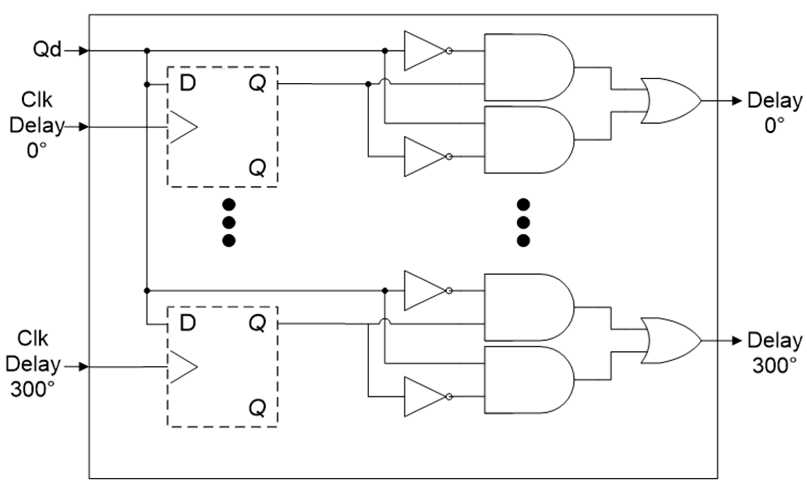
The CUT module consists of a Vi input, a clocking input (clk_cntrl), and an output (Qd). A D flip-flop is used to load a single bit of data into the FPGA in this work. The process of this module works as either positive gate triggered (PGT) or negative gate triggered (NGT), depending on the design requirement. The output of this CUT module is an input to the comparator module, which is the subsequent module shown in Figure 4. Within the comparator module, Qd is fed into two distinct sets of logic circuit elements; a group of memory elements from the CUT included the delay called Clk_Delay_x and another CUT set with the original signal input Vi. Signals from these two elements were then compared to detect whether any phase difference had occurred. A phase difference implies the occurrence of a delay. For example, if a phase difference between Qd and Clk_Delay_x is detected, Delay_x produces the output HIGH. The Delay_x output and Clk_Delay_x was fed into the last module called the phase shift detector module to identify the range in which the phase delay occurred.
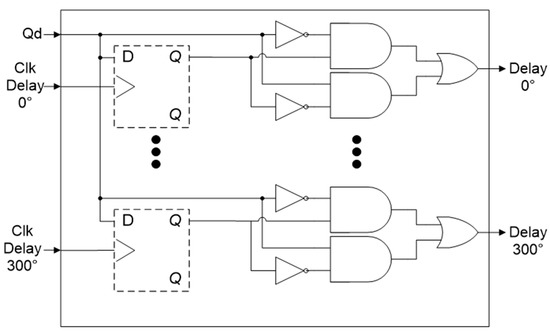
Figure 4.
Comparator module.
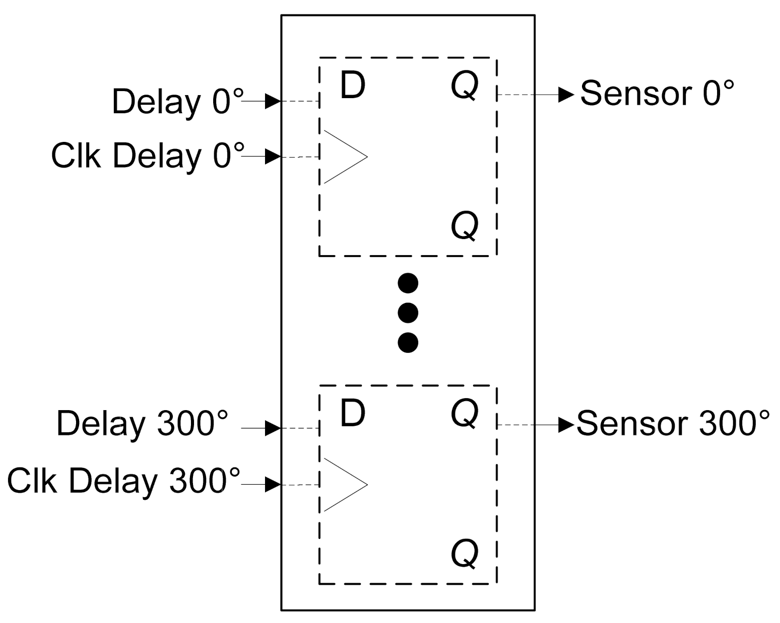
Figure 5 presents the phase shift detector module used to indicate the specific range of delays. The input signals for this module were fed from the comparator and clock delay modules. The Delay_300 signal must be paired with a clock called Clk_Delay_300 to determine whether the circuit detected the occurrence of a delay. The same applied to the other delays and clock signals for 0°, 50°, 100°, 150°, 200°, and 250°.
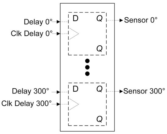
Figure 5.
Phase shift detector module.
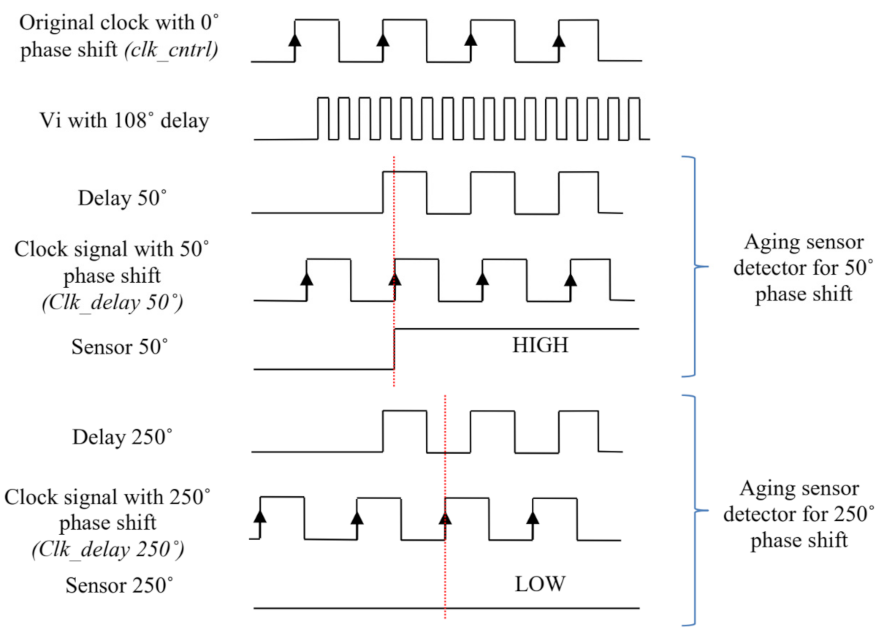
Figure 6 shows an example of the timing diagram obtained from the phase shift detector module for the delay detection of 50° and 250°. Initially, the synchronized clock clk_cntrl was fed to the CUT and clock delay modules. Next, the output produced from the CUT module Qd was compared with different phase shifts inside the comparator module. Then, the injected delay on the input signal Vi with a delay of 108° phase shift is illustrated for the detection process of the phase shift detector module. Finally, the Delay_x obtained from the Comparator circuit module was checked and tested using seven types of Clk_Delay for this injected delay signal. Therefore, the sensor types for each phase shift were HIGH for sensor 50° and LOW for sensor 250°.
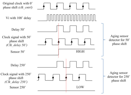
Figure 6.
Timing diagram to detect the phase delay for an aging signal.
3.1. Aging Detection Process
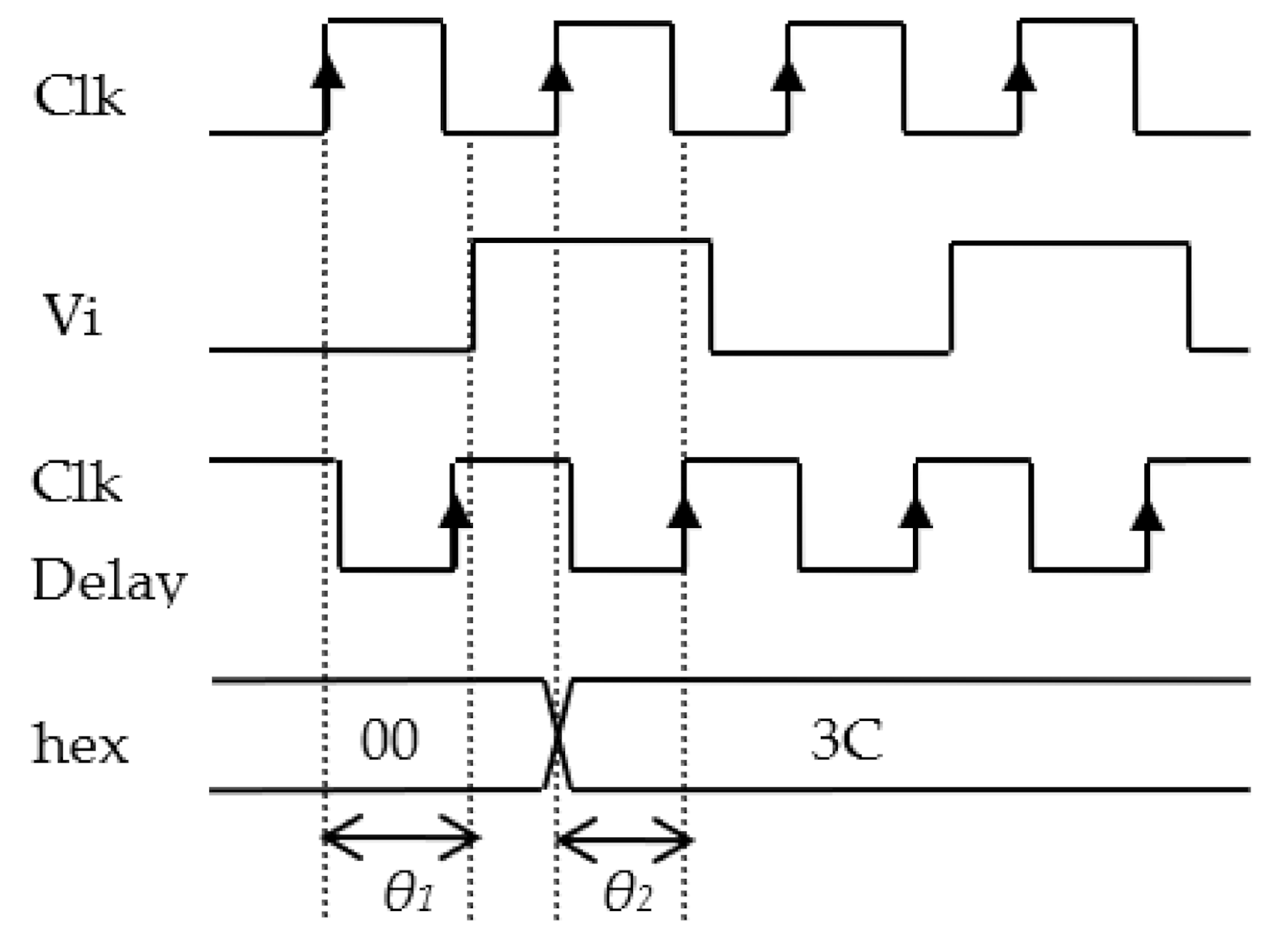
The process for detecting the delay is illustrated in Figure 7. The clock signal frequency is initially set for the system to be operated on a PGT or NGT, depending on the system requirement. The Vi is subsequently injected with a random delay signal to test the aging detection circuit. In the Verilog coding, the injected delay signal is present in the time unit using the ‘#’ symbol. For example, ‘#3′ equals three time units, equal to a 10.8° phase difference from the original signal. This injected delay signal signified the degradation caused by the variation of the threshold voltage, carrier mobility, NBTI, and HCI, as discussed in the previous section. Therefore, when the aging sensor detects the adjacent injected delay signals, these injected delay signals will fall in the same phase delay range and produce an identical output category. As shown in Figure 7, the Vi signal was preset with a delay of 220° for θ1 and a Clk_Delay of 200° for θ2.
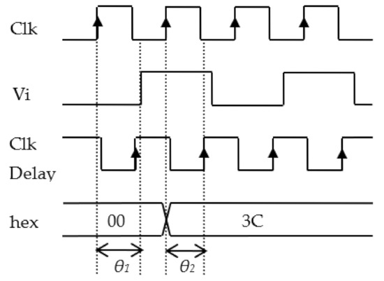
Figure 7.
Timing diagram to detect the phase delay.
Consequently, both θ values will be compared with the Vi signal independent of whether it exceeds the Clk_Delay frequency. To obtain an aging value, θ1 should be greater than θ2. For example, the 220° delay (Vi signal mentioned above) exceeded the 200° delay, which subsequently caused the delay detection to go HIGH. The output triggered a hex output signal as a reference value. The hex output signal is a data representation that is based on seven detection points, as previously described in Figure 5. The results obtained were in binary format and converted to a hexadecimal format called hex for a more straightforward implementation for the following process. However, if the value of θ1 is less than or equal to θ2, the aging sensor will produce a value of 0, indicating the aging condition is null.
Table 1 illustrates a sample of the detection process for the aging of the circuit using a sample Vi with delays of 220° and 270°. For θ1 = 220°, the Clk_Delay values for 50°, 100°, and 150° were HIGH, while other frequencies were LOW, hence producing an output of 3C16. Conversely for θ1 = 270°, the value of hex was 3E16 due to the Clk_Delay being HIGH for θ2 equal to 50°, 100°, 150°, 200°, and 250°.

Table 1.
Sample aging detection process.
3.2. Proposed Automatic Clock Correction
The delay degradation on the FPGA is continuously affected [54,55]. Therefore, it is crucial to correct the circuit automatically. Although the correction does not fully recover the chip, it is essential to maintain the efficiency and stability to provide a correct output.
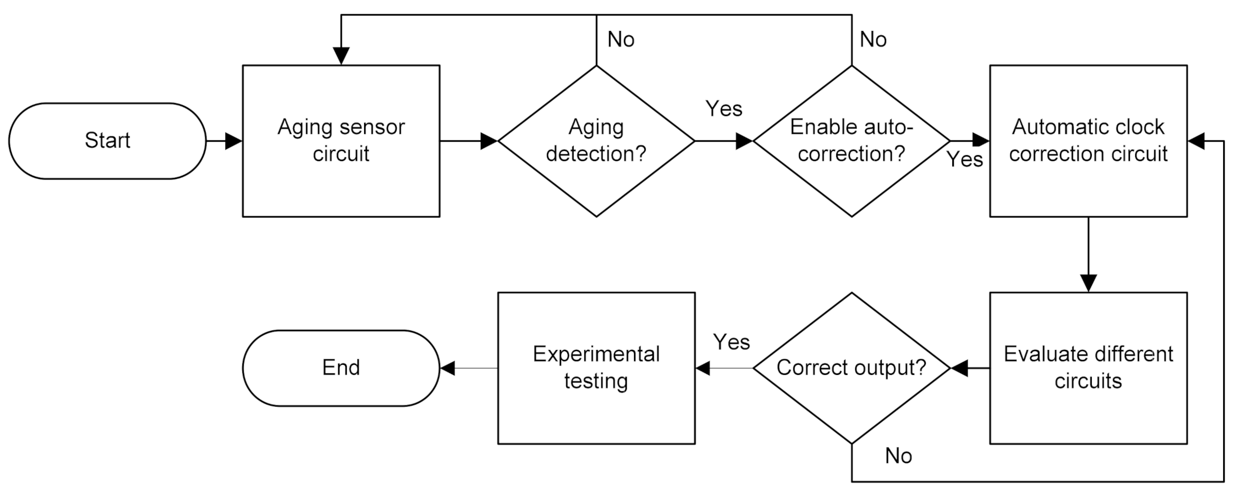
Automatic clock synchronization is a process of a centralized system that depends on the synchronized clock input. The clock synchronization is widely used in a wireless sensor network for correction purposes. Recent studies proposed several methodologies for performing clock correction, along with error correction for circuit design. M.G. Batarseh et al. digitized an analog signal and compared the signal to a reference value to maintain a near-zero error signal while focusing on the duty cycle obtained from the digital clock manager [56]. T. Anwar et al. supported this finding by developing a built-in error correction for the same clock cycles in FPGA cells [57]. Two clock correction algorithms called a Kalman filter and weighted-average-based NIST AT1 were investigated by A. Zenzinger et al. to detect failures and perform corrections from developed clock monitoring and a control unit [58]. This present work focused on automatic clock correction for an aging circuit, as shown in Figure 8. The circuit is illustrated in Figure 3 as a CUT module that aged or was injected with a substantial amount of delays was used to demonstrate the correction process. If aging is detected, the user can select either to enable the automatic clock correction input or not. The input signal then passes through the automatic clock correction circuit, which performs as a feedback circuit. The output waveform needs to be validated on the timing diagram to show that the correction process was made correctly. The output must indicate that there is no aging delay detected after a correction has been made. In order to validate this automated clock correction design, the proposed circuit was tested and evaluated experimentally for various types of combinational and sequential logic circuits, such as encoders, decoders, adders, and multiplexers.

Figure 8.
Flow chart for automatic clock correction.
A top module block diagram for the automated clock correction circuit is shown in Figure 9. The module consists of four inputs called Vi, enable, Clk, and rst and produces an output called out_as. First, the circuit is synchronized using a global clock that is fed with a standard clock signal Clk. The output of this global clock is fed into multiple clock generators, an automatic clock selector, the circuit under test, and enhanced phase shift detector modules. The combination of comparator and phase shift detector modules from Figure 3 are integrated into this enhanced phase shift detector module. Subsequently, the multiple clock generators module generates various types of stable clock signals, which were 0°/360°, 50°, 100°, 150°, 200°, 250°, and 300°. This module also has a reset signal rst for safety precautions and an input signal for the initialization process.

Figure 9.
Block diagram for automatic clock correction.
An automatic clock selector module selects the appropriate clock signal input according to the circuit specifications. By default, a phase of 0°/360° is set to trigger the circuit. This module consists of three inputs and produces a single output. The input signals originate from a previous module enable and a feedback signal from the top module output. The enable signal is used as an enable input to trigger the automatic clock correction. Meanwhile, the feedback signal provides the LUT values based on the detected signals from the corresponding seven detection points.
The CUT circuit can be substituted with various combinational logic circuits, such as encoders, decoders, and multiplexers. Thus, it is necessary to ensure that the number of bits used for inputs and outputs is the same for other modules. In addition, this automatic clock correction technique is applicable for any type of circuit, whether simple or complex. The Vi input signal is an input injected with delay signals. The rst input is used for the initialization process. The enhanced phase shift detector module consists of four inputs and a single output. The inputs Vi, clk, rst, and a reference signal from the CUT produce out_as with seven detection points. The input signal of Vi is compared with the reference signal to obtain the phase difference. This comparison is evaluated in terms of the point and phase that had caused the delay. Every bit of this enhanced phase shift detection is stored inside the memory element called hex, which is used as the feedback signal for correction purposes.
The lifetime of the FPGA can be extended by implementing this automated clock correction design via identifying the aging degradation followed by clock correction immediately. For example, if the remaining lifetime of the device is 12 months, it is possible to extend the lifetime for more than a year. In particular, the aging sensor detection process decayed the aging condition of the FPGA devices during the correction mode. The lifetime and automatic clock correction can be monitored based on the signal input called on. The input signal can be enabled periodically to reduce the delay degradation of the FGPA. For monitoring purposes, the switch can be turned off momentarily to view the remaining degradation. The delay cannot be eliminated; however, the usefulness of the device can be prolonged.
4. Comparison of Multiple Types of Delay Frequency
The aging sensor circuit, whose schematic is presented in Figure 3, produces a single output without aging and six outputs that indicate the delay that occurs at different clock frequencies and offer the aging status of the FPGA. The initial detection phase is from 0° and ends with 300° with intervals of 50° in between. All six of these phase delay detections will go HIGH if the CUT produces any form of delay. For example, if the CUT generates a delay of 108°, the indicators for 50° and 100° are to equal ‘1,’ while the indicators for 150°, 200°, 250°, and 300° will show a value of ‘0,’ as shown in Figure 10.

Figure 10.
Output result for the detection of θ1 = 108° of delay for voltage input Vi.
The design was tested using an exhaustive simulation test for all possible delays from 1.0° to 359°, as shown in Table 2. The results were created in binary and translated into hexadecimal values for more accessible analysis. For the delays between 1.0° and 50.0°, the output remained at 0016. The output only started to change when the delay was between 51.0° and 359.0°. The tabulated results show that when the delay occurred between 51.0° and 100.0°, the output value was 2016, while if the delay was between 201.0° and 250.0°, the output was 3C16, and so forth.

Table 2.
Output of aging detection using exhaustive test.
The simulation test discovered all possibilities of delay caused by the HCI and NBTI degradation effects that were monitored through critical path delay, interconnect delay, and propagation delay [59,60,61,62]. M. Sheng and J. Rose examined all these types of delays and found that the propagation delay on the FPGA is 41.3%, while the interconnect delay is58.7% [63]. These findings are supported by V. Manohararajah et al., who found that the interconnect delay was between 60 and 70% of the total delays [14], which leads to the lifetime degradation of the FPGA.
Based on the seven detection points of the delay degradation, the manufacturer of the FPGA provides a maximum lifespan of the FPGA as a reference purpose only [64] because the percentage utilization of the CLBs depends on the digital system developed. According to the Xilinx manufacturer of the Virtex-6, the lifetime for the 40 nm FPGA technology is 80 months [65]. Compared to other manufacturers, such as Altera and Lattice Semi, they reported that the lifetimes of their products Startix IV and ICE40L are around 36 months [66] and 24 months [67], respectively. Based on this information, the lifetime prediction was tabulated, as shown in Table 3. For example, if the delay detection was between 101° to 150°, the lifetime of the Xilinx FPGA will have 58.33% of its lifecycle remaining. In other words, the FPGA can be used for another 47 months. According to the desired lifetime specification, this calculation method will help the programmer replace the FPGA if necessary. The complete lifetime prediction calculated for each clock phase delay is shown in Table 3. The following formula was used to calculate the delay:
where %d is the percentage of delay and fd is the range of the phase delay. For example, if fd is between 101° and 150°, %d is equal to 41.67% by using the maximum value within this range, which is 150°. Subsequently, the following formula was used for calculating the remaining lifetime:
where Tr is the time remaining for the FPGA and LM is the maximum lifetime data provided by the FPGA manufacturer. For instance, with regard to the 40 nm Virtex-6 FPGA board with a %d of 41.67%, the LM is equal to 80 months; the calculated value of Tr is equal to 47 months.
%d = fd/360 × 100
Tr(months) = Lm − (%d × Lm)

Table 3.
Lifetime prediction for Xilinx, Altera, and Lattice Semi FPGAs.
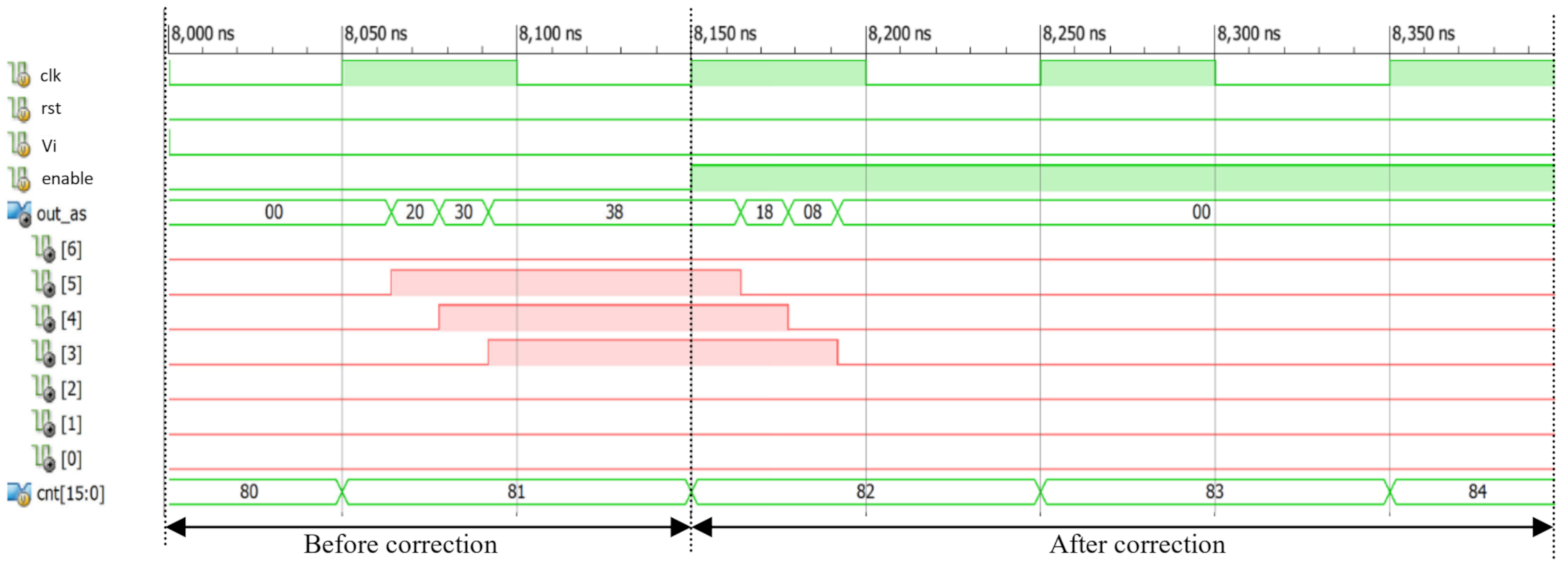
Figure 11 shows the output for the automatic clock correction aging sensor. For this proposed correction circuit, the enable input was set to 8150 . It is apparent from this figure that before the automatic clock correction was triggered for , the output waveform was in degradation mode. Interestingly, after , the out_as signals stabilized with no aging detected when enabled input was switched ON. These signals are highlighted in red.
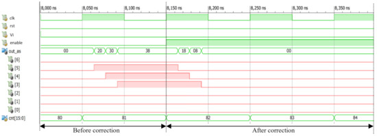
Figure 11.
Output result for detection with automatic clock correction.
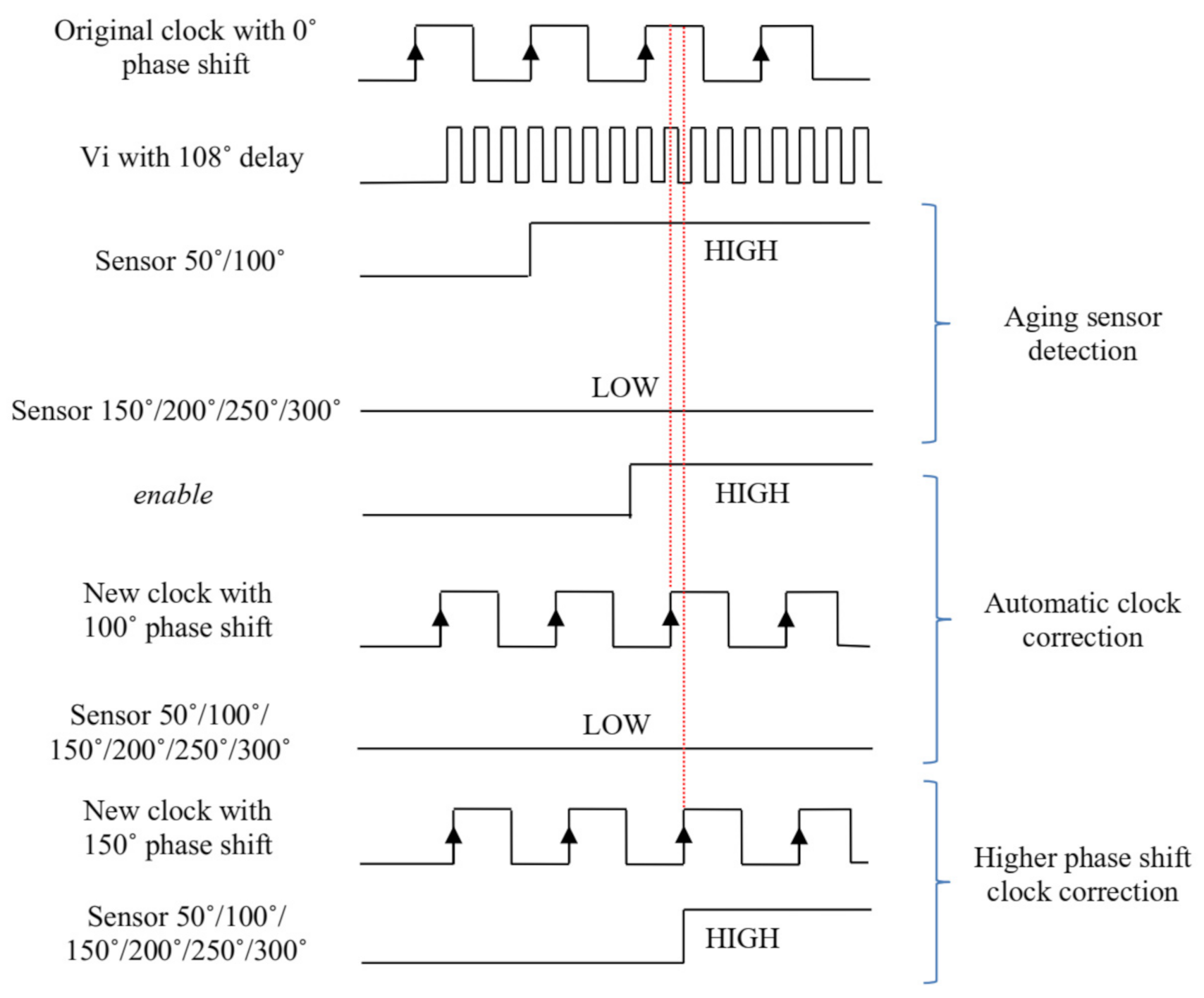
The automatic clock correction circuit was activated if the enable input was HIGH. During the activation period, the system will compensate for an appropriate clock signal input based on the occurrence of the delay. For example, based on the asterisk symbol (*) in Table 2, if the current delay phase was 108°, the clock signal for the system will automatically switch to 100°. Likewise, suppose the delay phase changes to 220° after several months or years. In this case, the clock signal will also automatically feed the system with 200°, which is as close to the delay phase without interruption by the user/programmer/designer. This process continues as long as the enable input remains HIGH for 360° delay degradation, covering all possibilities.
Figure 12 illustrates aging sensor detection and automatic clock correction processes with valid and invalid correction methods. Initially, the signal input Vi was injected with a 108° phase shift delay with the original clock input of a 0° phase shift. Since the 50° and 100° phase shifts of the aging sensors were less than the injected signal of the 108° phase shift, both of these sensors produced HIGH output signals. On the other hand, sensors 150°/200°/250°/300° had LOW output signals. The automatic clock correction was performed by triggering the enable input and a new clock signal of 100° phase shift was applied to the entire system. All aging sensors thus produced LOW output signals with a new clock signal used. If the new clock signal is higher than the signal input delay (Vi), all sensors will produce HIGH output signals. This invalid correction method is illustrated in Figure 12 with a clock signal with a 150° phase shift.
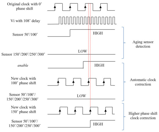
Figure 12.
Aging sensor detection and automatic clock correction with true and false correction processes.
Regarding the feedback signal obtained, the system performance was stable and did not degrade further. Therefore, the proposed automatic correction method can be beneficial for critical applications, such as medical, security, and satellite applications that require the system to be constantly stable. The design was tested for different sequential logic circuits, specifically T-Flip flops, JK Flip-flops, and ring counters, to verify that the design was applicable in various circuits. The testing method varied the number of bits used to cater for the signals for data, bytes, and words. It was observed that the proposed correction method could be considered as a guideline or a design consideration for system designers and industrial players to prolong the lifetimes of FPGA applications.
5. Experimental Validation
This section describes the validation process of simulation testing through experiments. After the simulation was implemented onto the FPGA board, the bit file was generated and downloaded onto the 40 nm Virtex-6 FPGA chip. The input and output configuration is shown in Table 4. First, the rst input was enabled for 1 s, followed by the Vi input signal. Subsequently, the automatic clock correction input called enable triggered the clock correction procedure for the entire FPGA system. This process was repeated for 100 random samples without a specific injected delay signal to validate the proposed design. The output observation on the 40 nm Virtex-6 ML605 FPGA board is shown in Figure 13. Figure 13a shows the initial setup for the experiment. Initially, all light-emitting diodes (LEDs) were in the OFF condition. Figure 13b shows that the rst input pin was enabled. This function was used to reset the entire FPGA system for preventive purposes. Figure 13c shows the input signal Vi as being enabled, which generated the random percentage delay aging to the multiple-point aging sensor module. For example, when the percentage delay was between and , the LEDs showed the values of . The LEDs were turned ON according to the aging detection, as stated earlier in Table 2. Finally, Figure 13d represents the automatic clock correction mode, whereby all LEDs were turned OFF and provided the best clock signal to the entire FPGA system.

Table 4.
Input and output configuration for the Virtex-6 ML605 FPGA board.
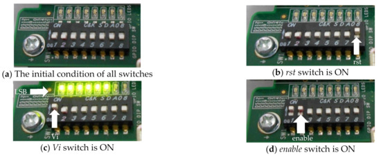
Figure 13.
Output result for the experiment on automatic clock correction.
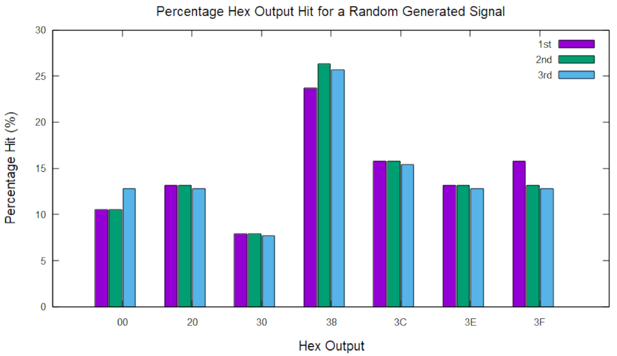
The percentages of hex output hits for the random signal generated for Vi are shown in Figure 14. The aging simulation was done for all possibilities of aging delays ranging from 1° to 359°, as illustrated in Figure 11. Furthermore, the exact design of the proposed aging sensor was embedded into FPGA, as described in Figure 13. The percentages of output hits were obtained through an experimental study. Initially, the Vi signal was randomly generated between 1° and 359° of aging with the delay signal. Then, this process was repeated and recorded with all potential aging signals generated. For the consistency verification of the aging sensor, the distribution of the measured seven hex outputs was repeated three times. From the chart, the coefficient of variation and standard variation were calculated to be 0.02% and 1.33%, respectively. Since the standard deviation was low, this implies that the data was close to the mean value, which verifies the reliability of the aging sensor proposed.

Figure 14.
Percentage hex output hit for the random generated signalfor three experiment repetitions.
Table 5 provides the mean percentage hit for different kinds of hex outputs, representing seven points of phase detection in line with the aging degradation based on the result obtained in Figure 14. The example stated earlier shows that the value of occupied approximately 13.90% of hits during the experimental testing. It shows that the design could be implemented for different aging processes. The results obtained covered all types of detection ranging from 0° to 360° according to the hex output.

Table 5.
Percentage of hex output hits for random delay signal generated.
As discussed earlier in Figure 2, the lifetime degradation was proportional to the delay degradation for the ring oscillator. It is known that the fundamental ring oscillator is constructed using CMOS, which is the same as the FPGA architecture. Therefore, Table 3 supports the idea that the percentage delay will increase due to the aging of the device according to the provided expected lifetime from the manufacturer. In addition, the experimental results show that the degradation in the FPGA was in line with CMOS degradation.
In summary, the evidence shows that the related degradation mechanism caused the FPGA to degrade while operating. The comparison of the aging sensor design with an automatic clock correction scheme is tabulated in Table 6. The proposed aging sensor with seven detection points could reduce the logic delay degradation on the 40 nm Virtex-6 FPGA. Thus, the experiment validated the result that the complexity of the multiple-point aging sensor with an automatic clock correction scheme is lower compared to other methods that use critical memory elements, several types of flip flops, and programmable delay circuits.

Table 6.
Comparison of aging sensor design with automated clock correction scheme.
6. Conclusions
Based on the simulation framework for the 40 nm technology node via a reliability simulator called the Eldo simulator, the effect of delay degradation on the FPGA was studied, along with aging sensor detection. The simulation results obtained from the Eldo simulator showed that the aging degradation over ten years shows a degradation trend of between 0.04 and 0.09% per year due to the NBTI degradation effect. Therefore, an aging sensor was implemented that detected seven points of aging degradation based on the phase shift delay. The results obtained from this aging sensor show that the degradation rate was 13.89% for each phase shift, which is in line with the NBTI degradation effect on the FPGA. For the optimization of the FPGA performance, the usage of the automatic clock correction scheme was vital to ensure that the output produced by the FPGA was consistently at the optimal level with a minimal delay effect. The experiment conducted on the 40 nm Virtex-6 FPGA also found that the coefficient of variation and standard deviation for the automatic clock correction scheme were 0.02% and 1.33%, respectively.
Therefore, the effect of the delay on the FPGA was mainly caused by the NBTI degradation effect, which can be translated into a lifetime prediction table that can help system designers and industrial users to replace the FPGA chip at the appropriate time. The data obtained were supported by several FPGA companies, such as Xilinx, Altera, and Lattice Semi. Based on the obtained results, it was shown that each FPGA had a different remaining lifetime due to the percentage utilization of the CLBs. Therefore, the delay retrieved from the FPGA had a performance shrinkage of about 13.89% for each 50° phase shift difference. This performance shrinkage showed that the effect of the NBTI on the 40 nm Virtex-6 FPGA occurred, although the technology size continues to shrink.
Author Contributions
A.J. designed and developed the aging sensor and wrote the original/revised drafts manuscript. N.S. and S.F.W.M.H. revised the manuscript and conducted data analysis of the research work. S.I.S. and Z.Z. verified data and conducted the statistical analysis. All authors have read and agreed to the published version of the manuscript.
Funding
This research received no external funding.
Institutional Review Board Statement
Not applicable.
Informed Consent Statement
Not applicable.
Data Availability Statement
Not applicable.
Acknowledgments
The authors would like to acknowledge the Faculty of Engineering at the University of Malaya and the Faculty of Electronics and Computer Engineering and Centre for Research and Innovation Management (CRIM) at the Universiti Teknikal Malaysia Melaka (UTeM) for financial support and technical contributions.
Conflicts of Interest
The authors declare no conflict of interest.
References
- Shamani, F.; Airoldi, R.; Ahonen, T.; Nurmi, J. FPGA implementation of a flexible synchronizer for cognitive radio applications. Conf. Des. Archit. Signal Image Process. DASIP 2015, 2015, 1–15. [Google Scholar] [CrossRef]
- Krasniewski, A. Evaluation of delay fault testability of LUT functions for improved efficiency of FPGA testing. Proc. Euromicro Symp. Digit. Syst. Des. 2001. [Google Scholar] [CrossRef]
- Lin, J.Y.; Chen, D.C.D.; Cong, J. Optimal simultaneous mapping and clustering for FPGA delay optimization. In Proceedings of the 43rd annual Design Automation, San Francisco, CA, USA, 24–28 July 2006; pp. 472–477. [Google Scholar] [CrossRef]
- Seng, K.P.; Lee, P.J.; Ang, L.M. Embedded intelligence on fpga: Survey, applications and challenges. Electronics 2021, 10, 895. [Google Scholar] [CrossRef]
- Fischer, T.; Amirante, E.; Huber, P.; Hofmann, K.; Ostermayr, M.; Schmitt-Landsiedel, D. A 65 nm test structure for SRAM device variability and NBTI statistics. Solid. State Electron. 2009, 53, 773–778. [Google Scholar] [CrossRef]
- Ghaderi, Z.; Ebrahimi, M.; Navabi, Z.; Bozorgzadeh, E.; Bagherzadeh, N. SENSIBle: A highly scalable sensor design for path-based age monitoring in FPGAs. IEEE Trans. Comput. 2017, 66, 919–926. [Google Scholar] [CrossRef]
- Tambara, L.A.; Kastensmidt, F.L.; Rech, P.; Frost, C. Decreasing FIT with diverse triple modular redundancy in SRAM-based FPGAs. In Proceedings of the IEEE International Symposium on Defect and Fault Tolerance in VLSI Systems, Amsterdam, The Netherlands, 1–3 October 2014; Volume 9, pp. 153–158. [Google Scholar] [CrossRef]
- Khaleghi, B.; Omidi, B.; Amrouch, H.; Henkel, J.; Asadi, H. Stress-aware routing to mitigate aging effects in SRAM-based FPGAs. In Proceedings of the FPL 2016 26th International Conference on Field Programmable Logic and Applications, Laussane, Switzerland, 29 August–2 September 2016. [Google Scholar] [CrossRef]
- Lee, K.; Wong, S.S. Fault-tolerant FPGA with column-based redundancy and power gating using RRAM. IEEE Trans. Comput. 2016, 2016, 409–414. [Google Scholar] [CrossRef]
- Wang, H.; Zhang, M.; Liu, Y. High-resolution digital-to-time converter implemented in an FPGA chip. Appl. Sci. 2017, 7, 52. [Google Scholar] [CrossRef]
- Srinivasan, S.; Mangalagiri, P.; Sarpatawi, K.; Xie, Y.; Vijaykrishnan, N. FLAW: FPGA Lifetime Awareness. In Proceedings of the 43rd ACM/IEEE Design Automation Conference, San Francisco, CA, USA, 24–28 July 2006; pp. 630–635. [Google Scholar]
- Maadi, M.; Bayram, B. Custom integrated circuit design for ultrasonic therapeutic CMUT array. Microsyst. Technol. 2015, 21, 875–891. [Google Scholar] [CrossRef]
- Bauer, L.; Braun, C.; Imhof, M.E.; Kochte, M.A.; Schneider, E.; Zhang, H.; Henkel, J.; Wunderlich, H.J. Test strategies for reliable runtime reconfigurable architectures. IEEE Trans. Comput. 2013, 62, 1494–1507. [Google Scholar] [CrossRef]
- Manohararajah, V.; Chiu, G.R.; Singh, D.P.; Brown, S.D. Predicting interconnect delay for physical synthesis in a FPGA CAD flow. IEEE Trans. Very Large Scale Integr. Syst. 2007, 15, 895–903. [Google Scholar] [CrossRef]
- Jaafar, A.; Soin, N.; Hatta, S.W.M. An educational FPGA design process flow using Xilinx ISE 13.3 project navigator for students. In Proceedings of the 2017 IEEE 13th International Colloquium on Signal Processing & Its Applications (CSPA), Penang, Malaysia, 10–12 March 2017. [Google Scholar] [CrossRef]
- Stott, E.; Cheung, P.; Sedcole, P. Fault tolerance and reliability in field-programmable gate arrays. IET Comput. Digit. Tech. 2010, 4, 196–210. [Google Scholar] [CrossRef]
- Zhang, H.; Bauer, L.; Kochte, M.A.; Schneider, E.; Wunderlich, H.-J.; Henkel, J. Aging resilience and fault tolerance in runtime reconfigurable architectures. IEEE Trans. Comput. 2017, 66, 957–970. [Google Scholar] [CrossRef]
- Moras, M.; Martin-Martinez, J.; Velayudhan, V.; Rodriguez, R.; Nafria, M.; Aymerich, X.; Simoen, E. Negative bias temperature instabilities in pMOSFETS: Ultrafast characterization and modelling. In Proceedings of the 2015 10th Spanish Conference on Electron Devices (CDE), Madrid, Spain, 11–13 February 2015. [Google Scholar] [CrossRef]
- Marquez-Viloria, D.; Castano-Londono, L.; Guerrero-Gonzalez, N. A modified knn algorithm for high-performance computing on fpga of real-time m-qam demodulators. Electronics 2021, 10, 627. [Google Scholar] [CrossRef]
- Chakravarthi, S.; Krishnan, A.T.; Reddy, V.; Machala, C.F.; Krishnan, S. A comprehensive framework for predictive modeling of negative bias temperature instability. In Proceedings of the 2004 IEEE International Reliability Physics Symposium, Phoenix, AZ, USA, 25–19 April 2004; pp. 273–282. [Google Scholar]
- Tu, R.H.; Rosenbaum, E.; Chan, W.Y.; Li, C.C.; Minami, E.; Quader, K.; Ko, P.K.; Hu, C. Berkeley Reliability Tools-BERT. IEEE Trans. Comput. Des. Integr. Circuits Syst. 1993, 12, 1524–1534. [Google Scholar] [CrossRef]
- Alnajjar, D.; Konoura, H.; Ko, Y.; Mitsuyama, Y.; Hashimoto, M.; Onoye, T. Implementing flexible reliability in a coarse-grained reconfigurable architecture. IEEE Trans. Very Large Scale Integr. Syst. 2013, 21, 2165–2178. [Google Scholar] [CrossRef]
- Cho, M.; Roussel, P.; Kaczer, B.; Degraeve, R.; Franco, J.; Aoulaiche, M.; Chiarella, T.; Kauerauf, T.; Horiguchi, N.; Groeseneken, G. Channel hot carrier degradation mechanism in long/short channel n-FinFETs. IEEE Trans. Electron. Devices 2013, 60, 4002–4007. [Google Scholar] [CrossRef]
- Cha, S.; Liu, T.; Milor, L. Negative bias temperature instability and gate oxide breakdown modeling in circuits with die-to-die calibration through power supply and ground signal measurements. IEEE Trans. Very Large Scale Integr. Syst. 2017, 25, 2271–2284. [Google Scholar] [CrossRef]
- Kumar, S.V.; Kim, C.H.; Sapatnekar, S.S. An analytical model for negative bias temperature instability. Int. Conf. Comput. Aided Des. 2006, 493–496. Available online: http://ieeexplore.ieee.org/xpls/abs_all.jsp?arnumber=4110220 (accessed on 19 April 2014). [CrossRef]
- Leong, C.; Semião, J.; Teixeira, I.C.; Santos, M.B.; Teixeira, J.P.; Valdes, M.; Freijedo, J.; Rodríguez-Andina, J.J.; Vargas, F. Aging monitoring with local sensors in FPGA-based designs. In Proceedings of the 23rd International Conference on Field programmable Logic and Applications, Porto, Portugal, 2–4 September 2013. [Google Scholar] [CrossRef]
- Amouri, A.; Hepp, J.; Tahoori, M. Built-in self-heating thermal testing of FPGAS. IEEE Trans. Comput. Des. Integr. Circuits Syst. 2016, 35, 1546–1556. [Google Scholar] [CrossRef]
- Tahoori, M.B.; Kiamehr, S.; Firouzi, F.; Ebrahimi, M. Extending standard cell library for aging mitigation. IET Comput. Digit. Tech. 2015, 9, 206–212. [Google Scholar] [CrossRef]
- Chan, T.B.; Chan, W.T.J.; Kahng, A.B. On aging-aware signoff for circuits with adaptive voltage scaling. IEEE Trans. Circuits Syst. I Regul. Pap. 2014, 61, 2920–2930. [Google Scholar] [CrossRef][Green Version]
- Shah, S.; Yadav, A.P.; Beohar, N.; Vishvakarma, A. Process variations tolerant subthreshold Darlington pair based NBTI sensor circuit. IET Comput. Digit. Tech. 2018, 13, 243–249. [Google Scholar] [CrossRef]
- Valdes-Pena, M. Design and validation of configurable online aging sensors in nanometer-scale FPGAs. IEEE Trans. Nanotechnol. 2013, 12, 508–517. [Google Scholar] [CrossRef]
- Ebrahimi, M.; Navabi, Z. Selecting Representative critical paths for sensor placement provides early FPGA aging information. IEEE Trans. Comput. Des. Integr. Circuits Syst. 2019, 39, 2976–2989. [Google Scholar] [CrossRef]
- Sai, G.; Zwolinski, M.; Halak, B. A cost-efficient aging sensor based on multiple paths delay fault monitoring. In Ageing of Integrated Circuits; Springer: Cham, Switzerland, 2020. [Google Scholar]
- Christoph, R.; Andreas, A.; Happe, M.; Plessl, C. Exploration of ring oscillator design space for temperature measurements on FPGAs. In Proceedings of the 22nd International Conference on Field Programmable Logic and Applications (FPL), Oslo, Norway, 29–31 August 2012; pp. 559–562. Available online: http://ieeexplore.ieee.org/xpl/mostRecentIssue.jsp?punumber=6330714 (accessed on 16 January 2016).
- Shafiee, N.; Tewari, S.; Calhoun, B.; Shrivastava, A. Infrastructure circuits for lifetime improvement of ultra-low power IoT devices. IEEE Trans. Circuits Syst. I Regul. Pap. 2017, 64, 2598–2610. [Google Scholar] [CrossRef]
- Suh, J.; Member, S.; Suda, N.; Member, S.; Xu, C.; Hakim, N. Programmable analog device array (PANDA): A methodology for transistor-level analog emulation. IEEE Trans. Circuits Syst. I Regul. Pap. 2013, 60, 1369–1380. [Google Scholar] [CrossRef]
- Cao, Y.K. Predictive Technology Model. 2017. Available online: http://ptm.asu.edu/ (accessed on 30 July 2017).
- Mentor Graphics Corporation. Eldo® Platform User’s Manual; Mentor Graphics Corporation: Wilsonville, OR, USA, 2017. [Google Scholar]
- Fang, J.; Sapatnekar, S.S. Incorporating hot-carrier injection effects into timing analysis for large circuits. IEEE Trans. Very Large Scale Integr. Syst. 2014, 22, 2738–2751. [Google Scholar] [CrossRef]
- Zhang, H.; Liu, C.; Wang, T.; Zhang, H.; Zeng, C. Analysis of hot carrier and NBTI induced device degradation on CMOS ring oscillator. In Proceedings of the 3rd International Conference on Consumer Electronics, Communications and Networks, Xianning, China, 20–22 November 2013; pp. 141–144. [Google Scholar] [CrossRef]
- Kim, Y.; Shim, H.; Jin, M.; Bae, J.; Liu, C.; Pae, S. Investigation of HCI effects in FinFET based ring oscillator circuits and IP Blocks. In Proceedings of the IEEE International Reliability Physics Symposium (IRPS), Monterey, CA, USA, 2–6 April 2017; Volume 2131, pp. 2–5. [Google Scholar] [CrossRef]
- Singh, P.; Karl, E.; Sylvester, D.; Blaauw, D. Dynamic NBTI management using a 45 nm multi-degradation sensor degradation in ICs. IEEE Trans. Circuits Syst. I Regul. Pap. 2010, 1, 1–49. [Google Scholar]
- Wang, W. Circuit Aging in Scaled CMOS Design Modeling Simulation and Prediction; Arizona State University: Phoenix, AZ, USA, 2008. [Google Scholar]
- Hussin, H.; Soin, N.; Bukhori, M.F.; Wahab, Y.A.; Shahabuddin, S. New simulation method to characterize the recoverable component of dynamic negative-bias temperature instability in p-channel metal-oxide-semiconductor field-effect transistors. J. Electron. Mater. 2014, 43, 1207–1213. [Google Scholar] [CrossRef]
- Alimin, A.F.M.; Radzi, A.A.M.; Sazali, N.A.F.; Hatta, S.F.W.M.; Soin, N.; Hussin, H. Influence of design and process parameters of 32-nm advanced-process high-kp-MOSFETs on negative-bias temperature instability and study of defects. J. Electron. Mater. 2017, 46, 5942–5949. [Google Scholar] [CrossRef]
- Sengupta, D.; Sapatnekar, S. Estimating circuit aging due to BTI and HCI using ring-oscillator-based sensors. IEEE Trans. Comput. Des. Integr. Circuits Syst. 2017, 36, 1688–1701. [Google Scholar] [CrossRef]
- Hyams, D.G. CurveExpert software. 2010. Available online: http://www.curveexpert.net/ (accessed on 3 November 2017).
- Schlunder, C.; Aresu, S.; Georgakos, G. HCI vs. BTI? Neither one’s out. In Proceedings of the IEEE International Reliability Physics Symposium (IRPS), Anaheim, CA, USA, 15–19 April 2012; pp. 1–6. [Google Scholar]
- Bravaix, A.; Guerin, C.; Huard, V.; Roy, D.; Roux, J.M.; Vincent, E. Hot-carrier acceleration factors for low power management in DC-AC stressed 40 nm NMOS node at high temperature. In Proceedings of the IEEE International Reliability Physics Symposium, Montreal, QC, Canada, 26–30 April 2009; pp. 531–548. [Google Scholar]
- Liu, C.Q.; Cao, Y.; Chang, C.H. ACRO-PUF: A Low-power, reliable and aging-resilient current starved inverter-based ring oscillator physical unclonable function. IEEE Trans. Circuits Syst. I Regul. Pap. 2017, 64, 3138–3149. [Google Scholar] [CrossRef]
- Kohno, T.; Broido, A.; Claffy, K.C. Remote physical device fingerprinting. IEEE Trans. Dependable Secur. Comput. 2005, 2, 93–108. [Google Scholar] [CrossRef]
- Murdoch, S. Hot or not: Revealing hidden services by their clock skew. In Proceedings of the 13th ACM Conference on Computer and Communications Security 2006, Alexandria, VA, USA, 30 October–3 November 2006; pp. 27–36. [Google Scholar]
- Xilinx Corporation. LogiCORE IP Clocking Wizard; Version 3.2; Xilinx Corporation: San Jose, CA, USA, 2011. [Google Scholar]
- Floyd, L.; O’Reilly, M.; Mathewson, A. Delay simulation comparisons between A1/SiO2 and Cu/BCB multilevel interconnect. Microelectron. Eng. 1997, 33, 415–422. [Google Scholar] [CrossRef]
- Steinlesberger, G.; Traving, M.; Engelhardt, M. Scaling of parasitics and delay times in the backend-of-line. Microelectron. Eng. 2003, 70, 7–12. [Google Scholar]
- Batarseh, M.G.; Al-Hoor, W.; Huang, L.; Iannello, C.; Batarseh, I. Window-masked segmented digital clock manager-FPGA-based digital pulsewidth modulator technique. IEEE Trans. Power Electron. 2009, 24, 2649–2660. [Google Scholar] [CrossRef]
- Anwar, T.; Lala, P.K.; Parkerson, J.P. A novel FPGA Architecture with built-in error correction. Instrum. Meas. Technol. Conf. 2007, 1–4. [Google Scholar] [CrossRef]
- Zenzinger, A.; Bartusch, T.; Kuehl, C.; Fischer, S.; Shrestha, A. Failure detection and correction for clock ensemble in space. In Proceedings of the 6th ESA Workshop on Satellite Navigation Technologies (Navitec 2012) & European Workshop on GNSS Signals and Signal Processing, Noordwijk, The Netherlands, 5–7 December 2012; pp. 1–8. [Google Scholar] [CrossRef]
- Qiao, F.; He, Y.; Ai, L.; Zhang, G.; Zhang, X. A comprehensive NBTI degradation model based on ring oscillator circuit. In Proceedings of the 12th IEEE International Conference on Solid-State and Integrated Circuit Technology (ICSICT), Guilin, China, 28–31 October 2014; Volume 2, pp. 1–3. [Google Scholar]
- Luo, Y.H.; Nayak, D.; Lee, J.; Gitlin, D.; Tsai, C.T. Reliability of strain-Si FPGA product fabricated by novel ultimate spacer process. In Proceedings of the IEEE International Integrated Reliability Workshop Final Report, South Lake Tahoe, CA, USA, 16 October–19 September 2006; pp. 175–178. [Google Scholar] [CrossRef]
- Sideris, I.; Pekmestzi, K. A column parity based fault detection mechanism for FIFO buffers. Integr. VLSI J. 2013, 46, 265–279. [Google Scholar] [CrossRef]
- Jaafar, A.; Soin, N.; Hatta, S.W.M.; Md, S.S.I. Delay performance due to thermal variation on field-programmable gate array via the adoption of a stable ring oscillator. IET Comput. Digit. Tech. 2019, 1–9. [Google Scholar] [CrossRef]
- Sheng, M.; Rose, J. Mixing buffers and pass transistors in FPGA routing architectures. In Proceedings of the 2001 ACM/SIGDA Ninth International Symposium on Field Programmable Gate Arrays; Association for Computing Machinery: New York, NY, USA, 2001; pp. 75–84. [Google Scholar] [CrossRef]
- Altera Corporation. Guaranteeing Silicon Performance with FPGA Timing Models. Altera Doc. 2010. Available online: https://www.altera.com/content/dam/altera-www/global/en_US/pdfs/literature/wp/wp-01139-timing-model.pdf (accessed on 28 January 2021).
- Xilinx Corporation. Xilinx Reliability Report; Xilinx Corporation: San Jose, CA, USA, 2015. [Google Scholar]
- Intel Corporation. Reliability Report 58. 2014. Available online: https://www.intel.co.jp/content/www/jp/ja/programmable/documentation/reliability-report.html?wapkw=reliability%20report (accessed on 18 May 2015).
- Lattice Semiconductor. Lattice Products Reliability Report. 2013. Available online: https://www.latticesemi.com/-/media/LatticeSemi/Documents/QualityAssurance/OZ/Product-Reliability-Monitor-Report.ashx?document_id=50307 (accessed on 18 May 2015).
Publisher’s Note: MDPI stays neutral with regard to jurisdictional claims in published maps and institutional affiliations. |
© 2021 by the authors. Licensee MDPI, Basel, Switzerland. This article is an open access article distributed under the terms and conditions of the Creative Commons Attribution (CC BY) license (https://creativecommons.org/licenses/by/4.0/).

