
Isomorphic Circuits of Independent Amplitude Tunable Voltage-Mode Bandpass Filters and Quadrature Sinusoidal Oscillators


Abstract
:1. Introduction
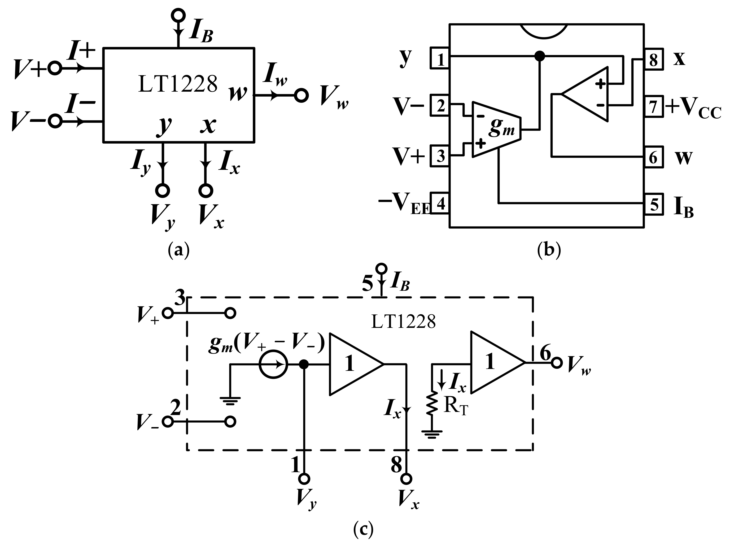
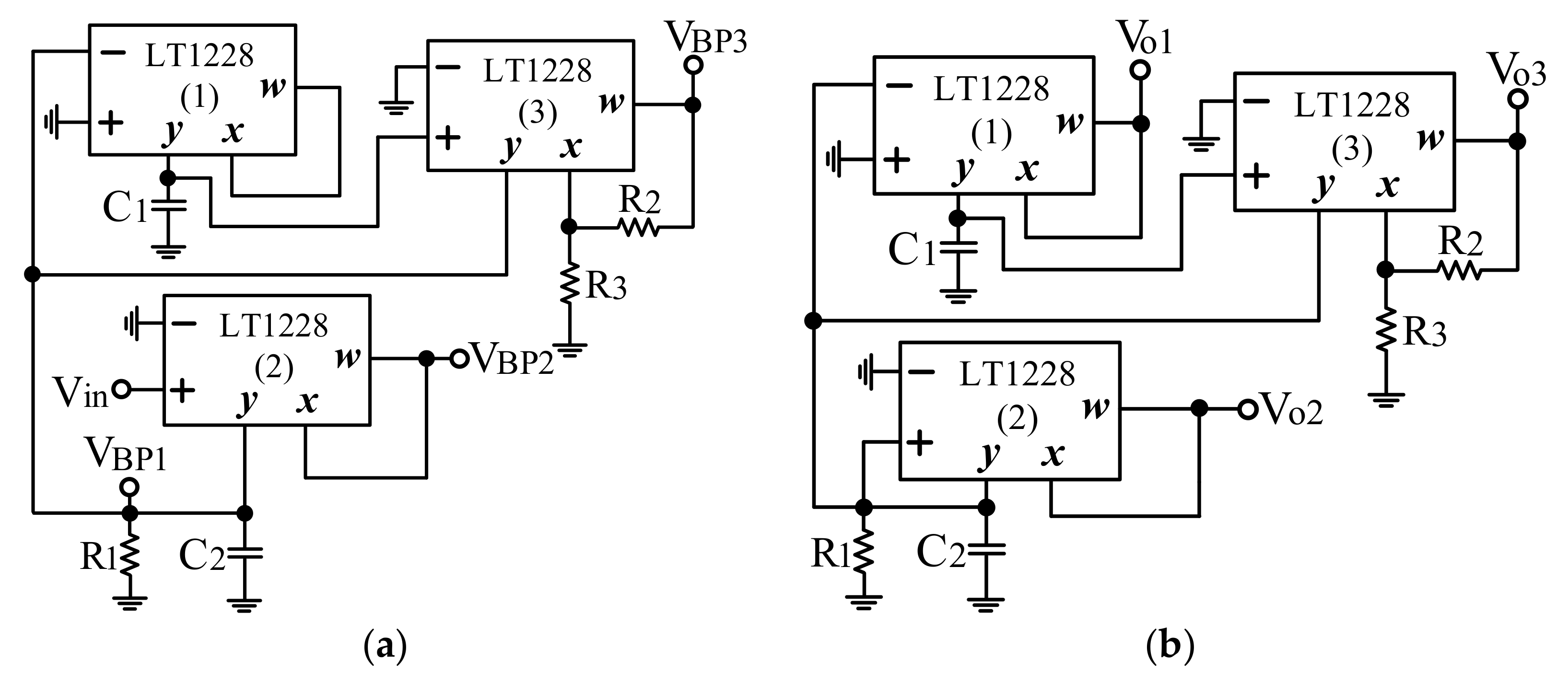
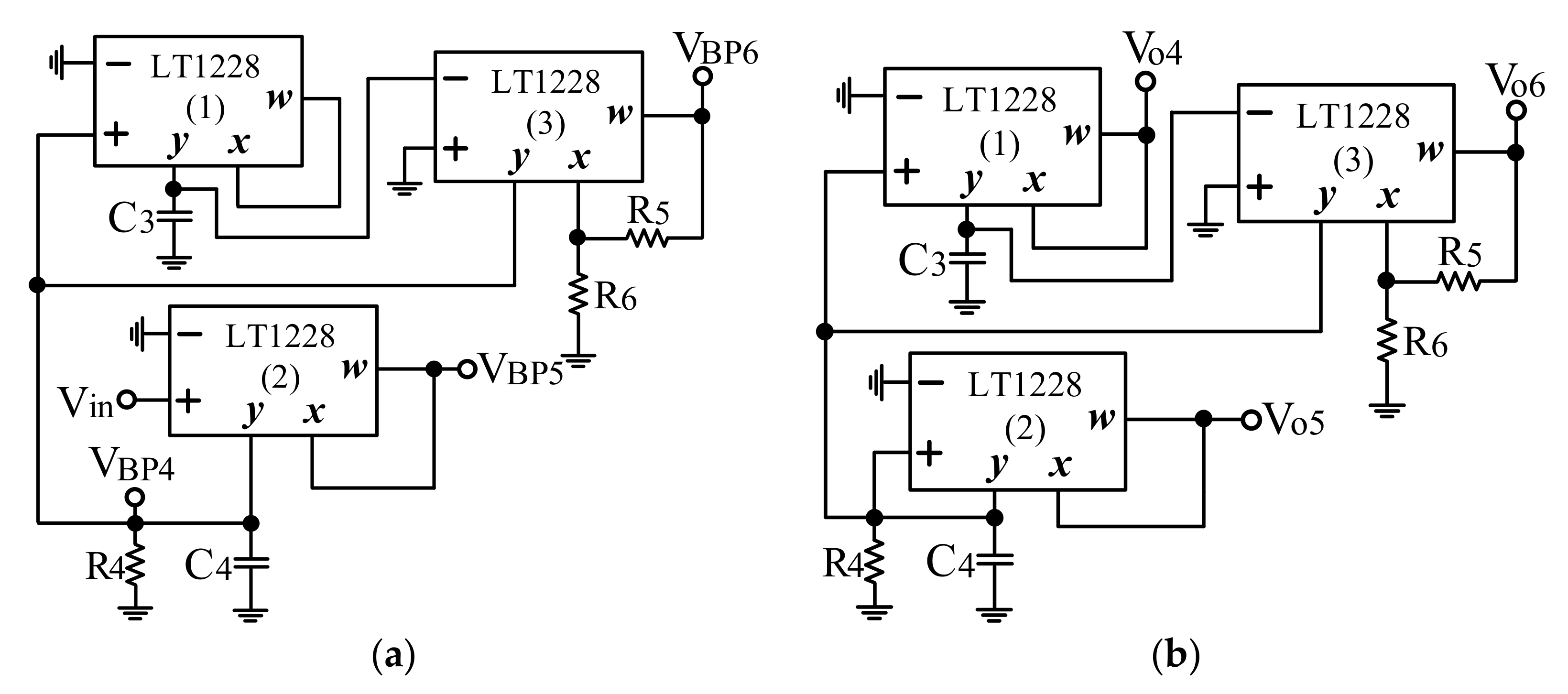
2. The Proposed Isomorphic Circuits
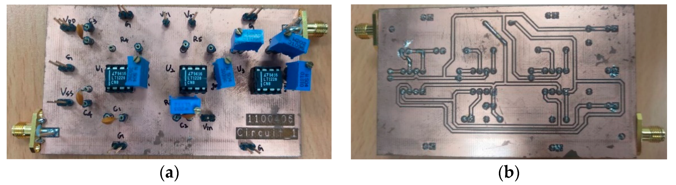
3. Simulation and Experimental Measurements
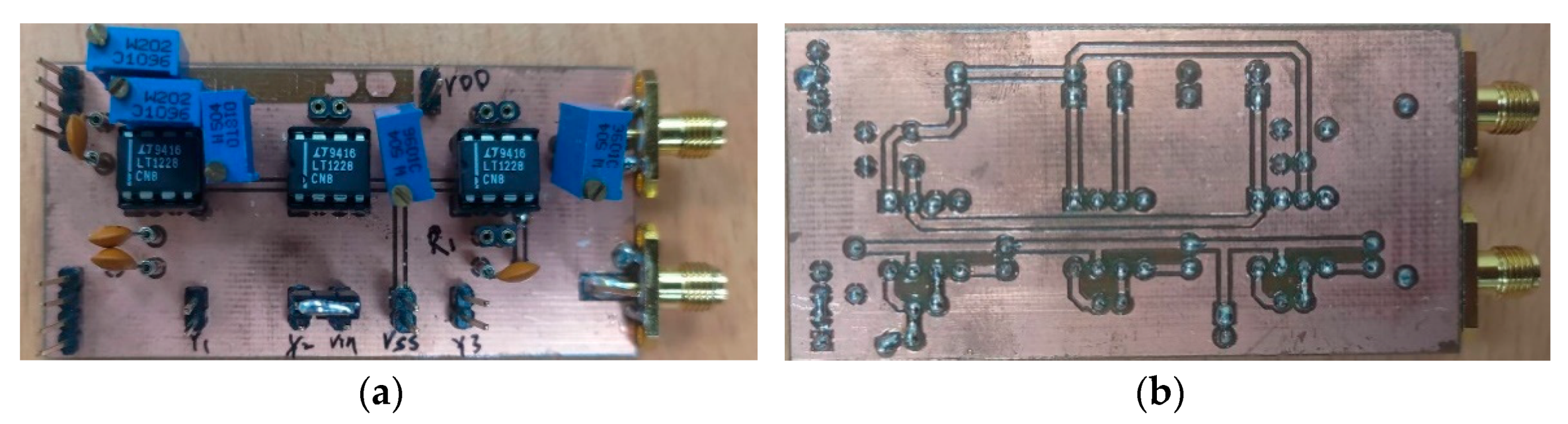
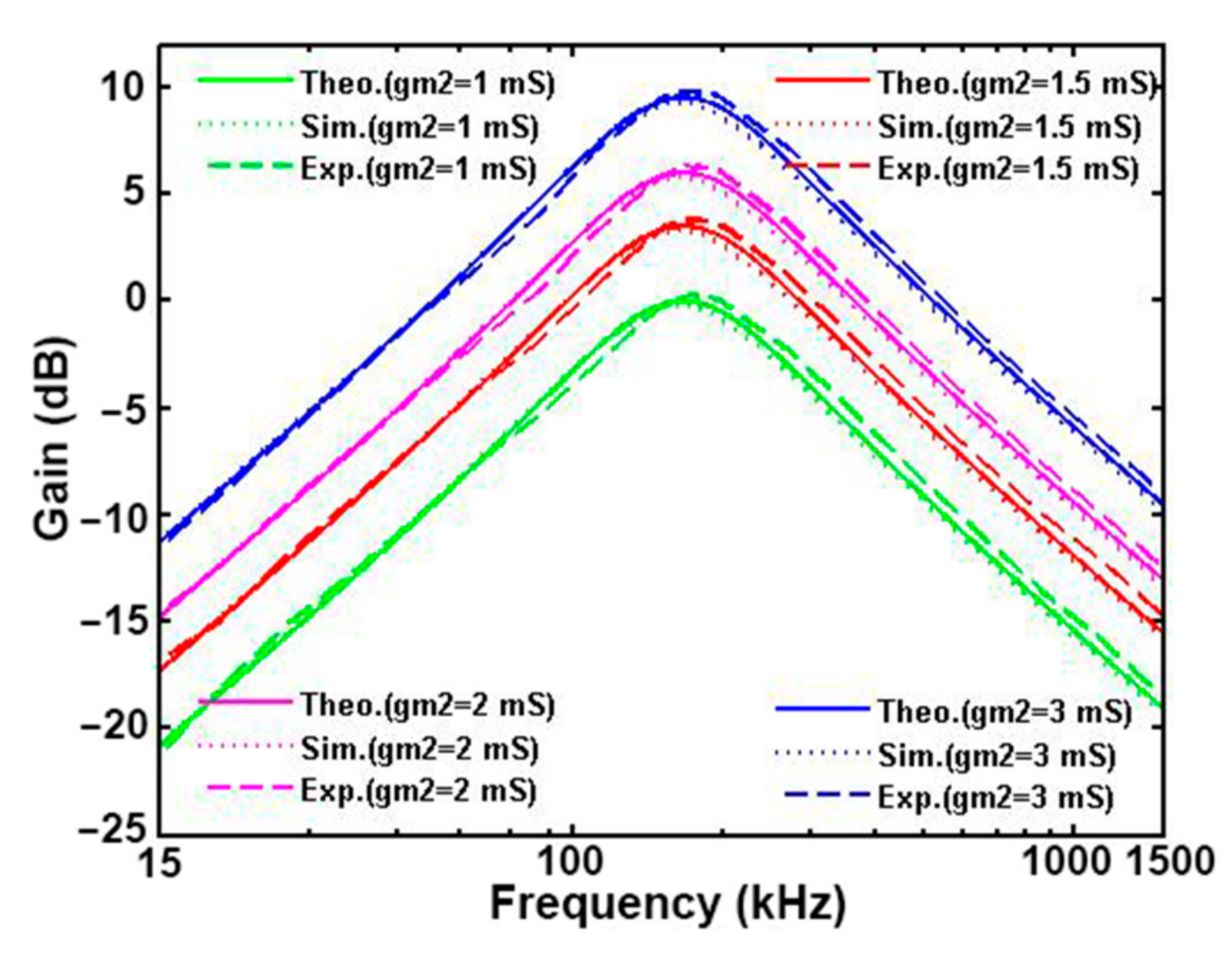
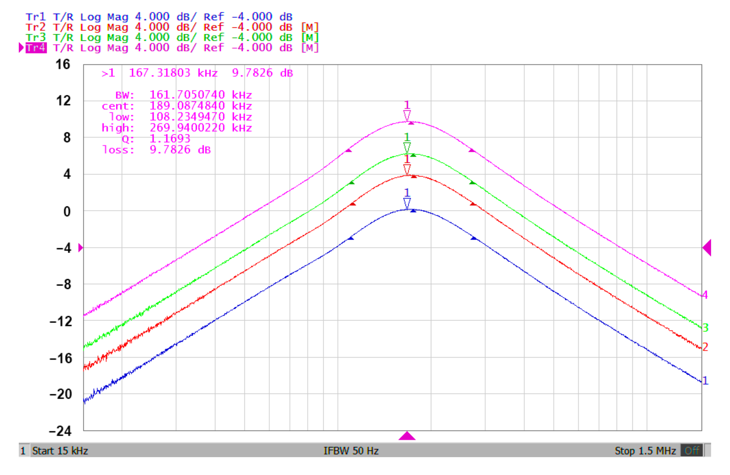
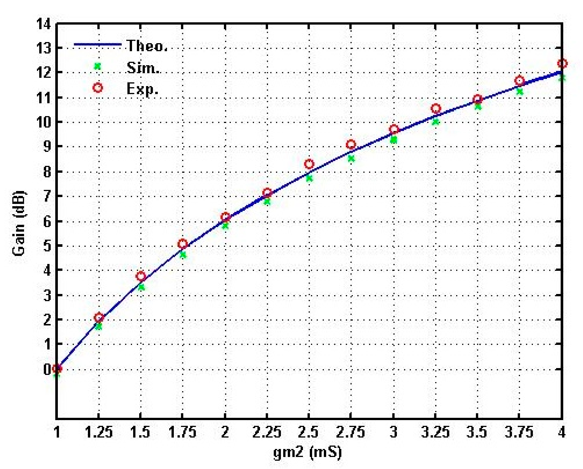
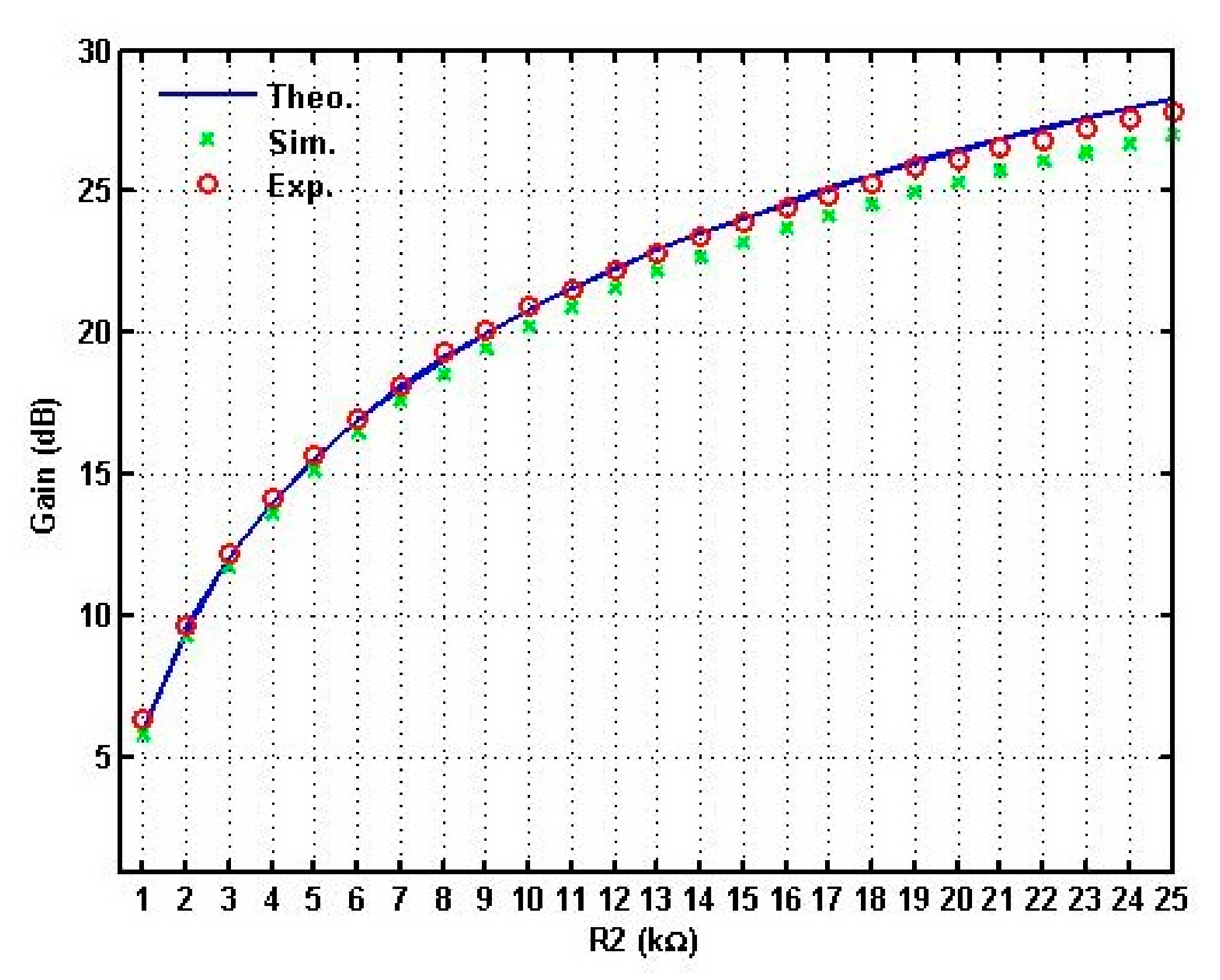
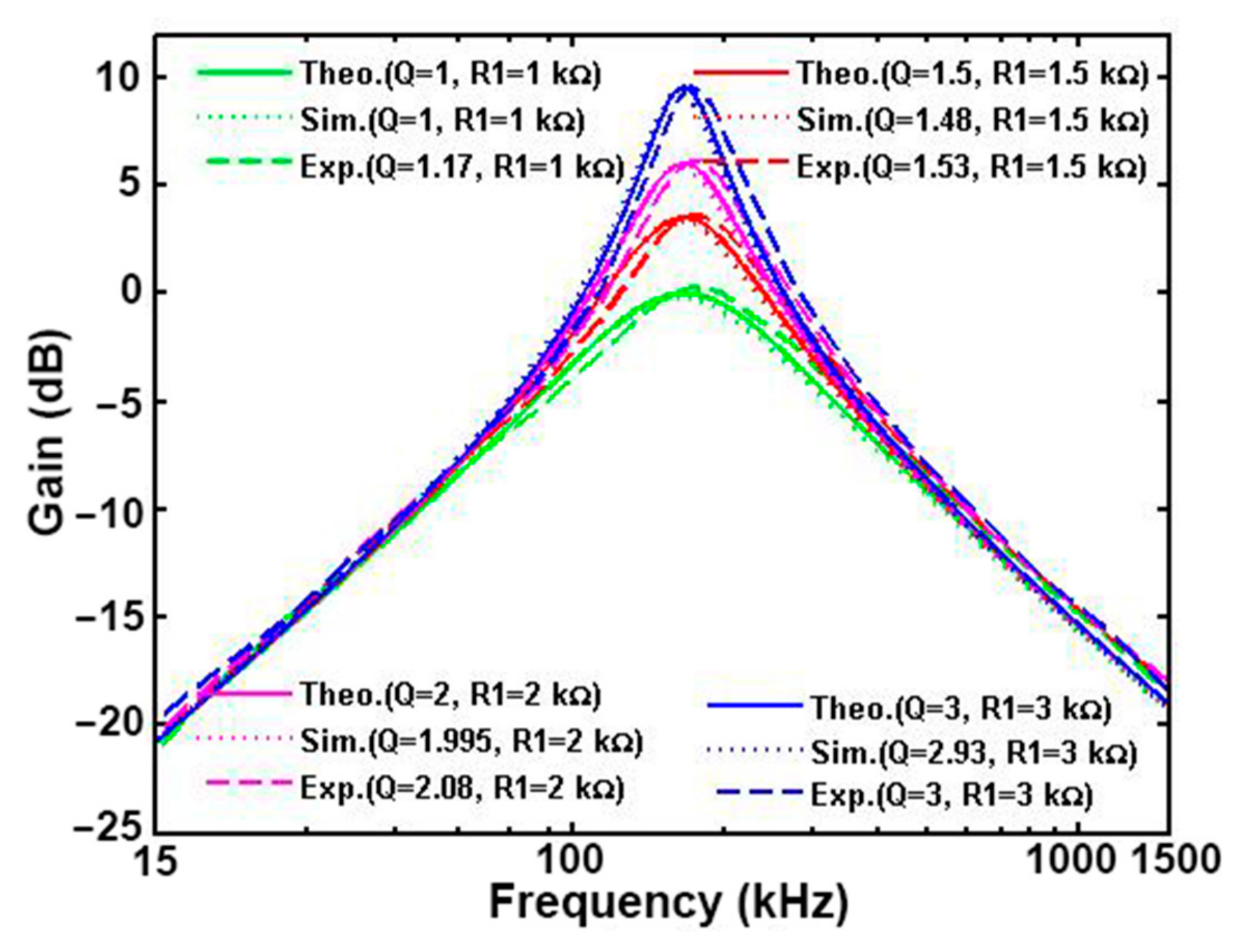
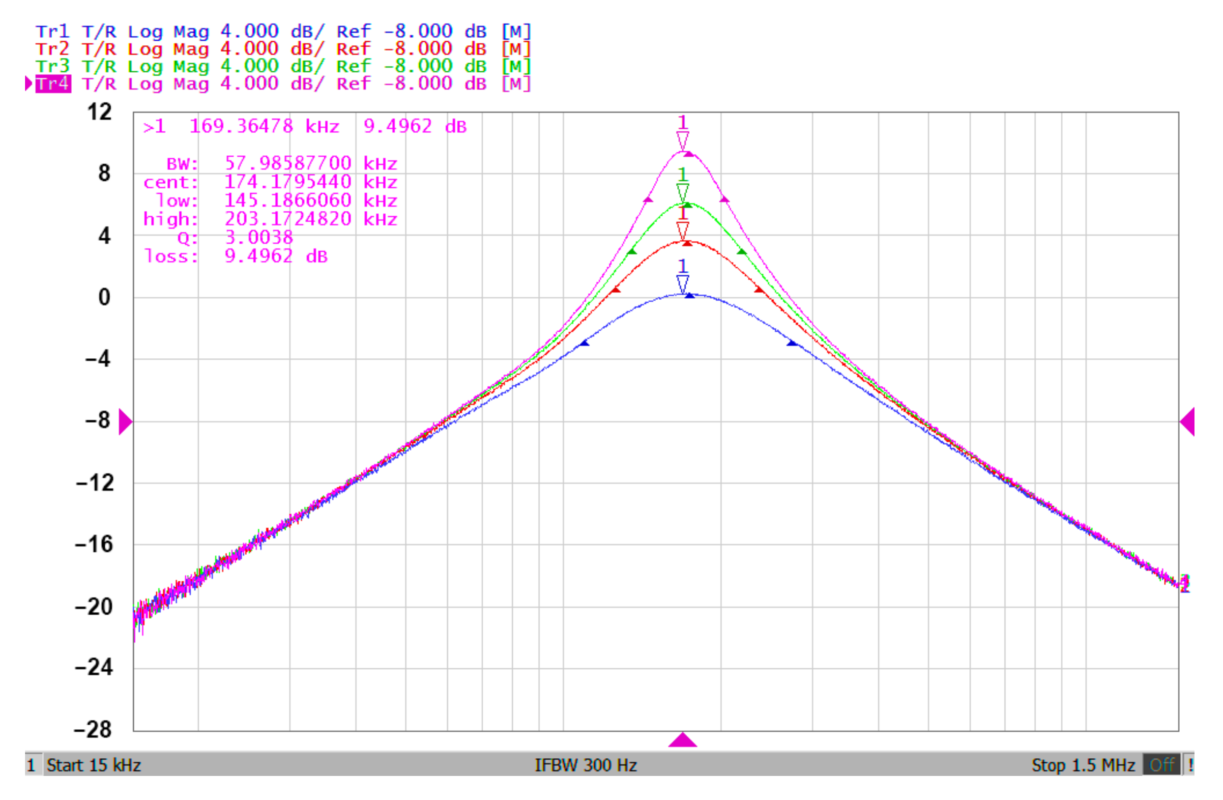
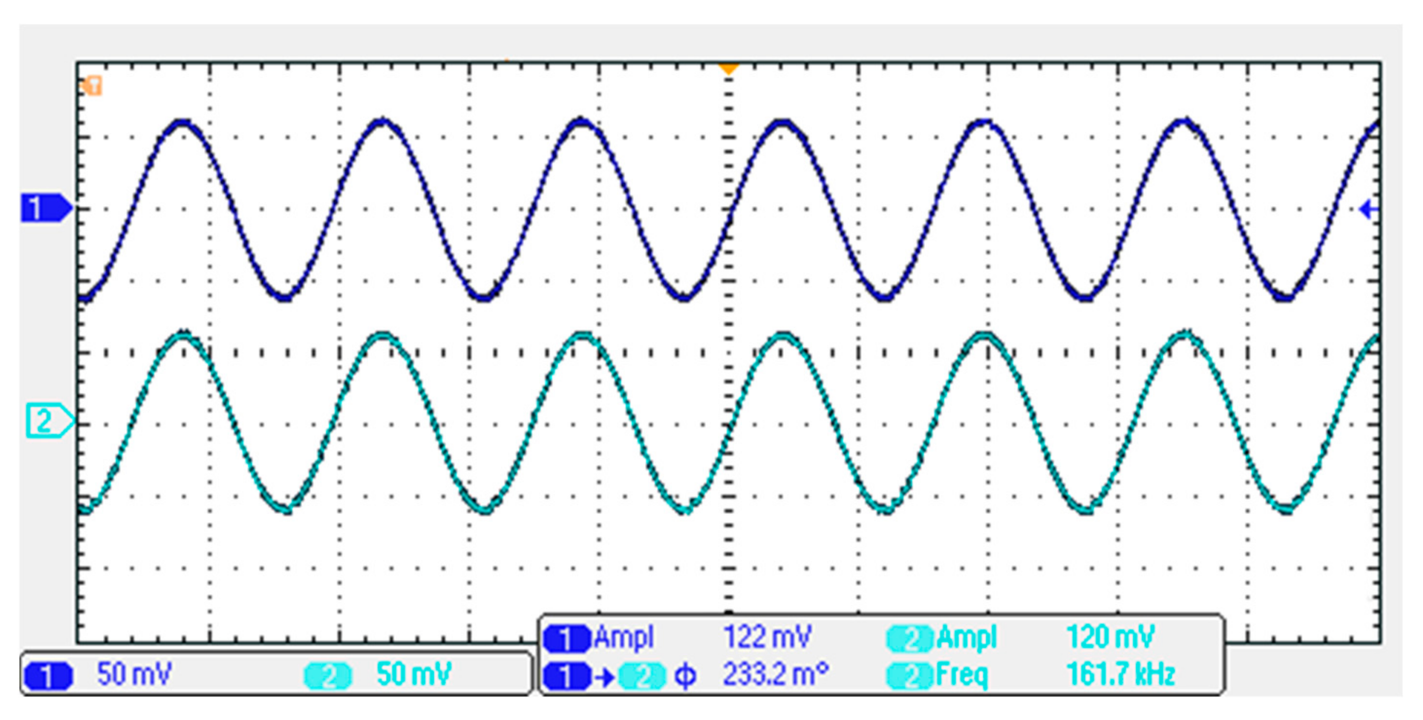
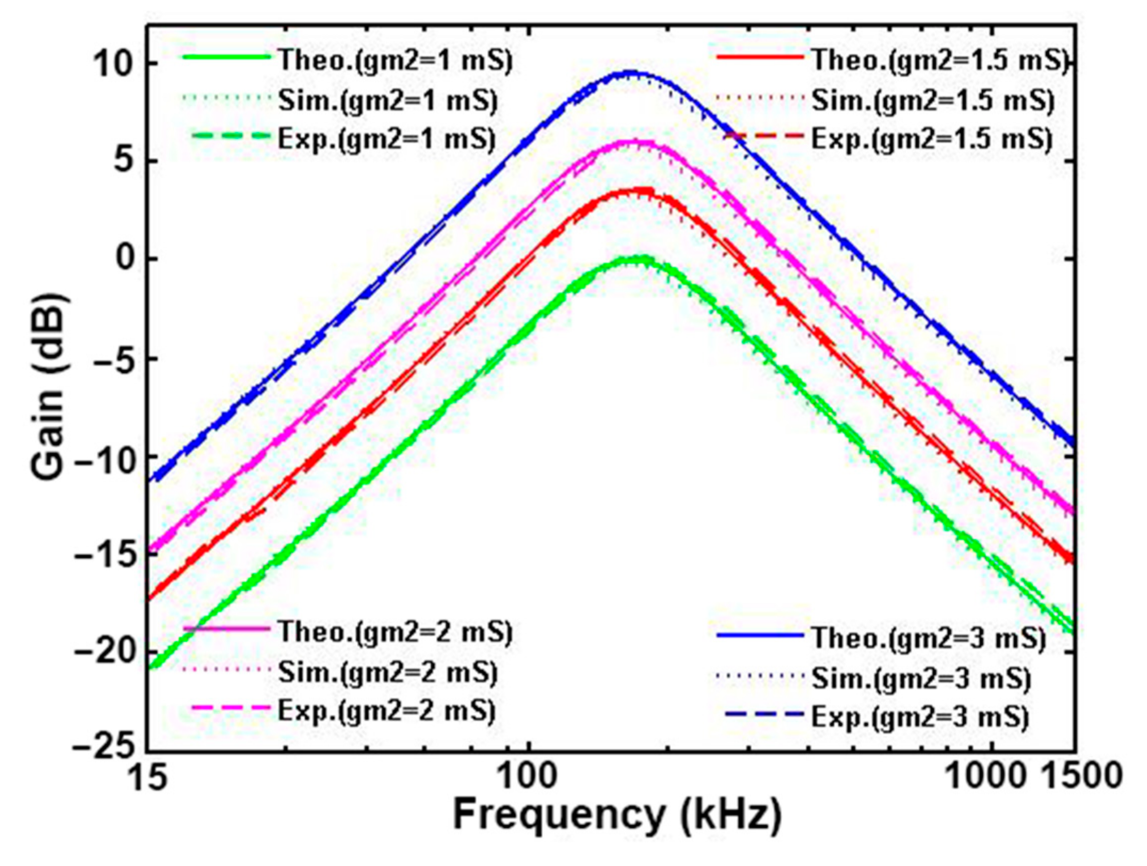
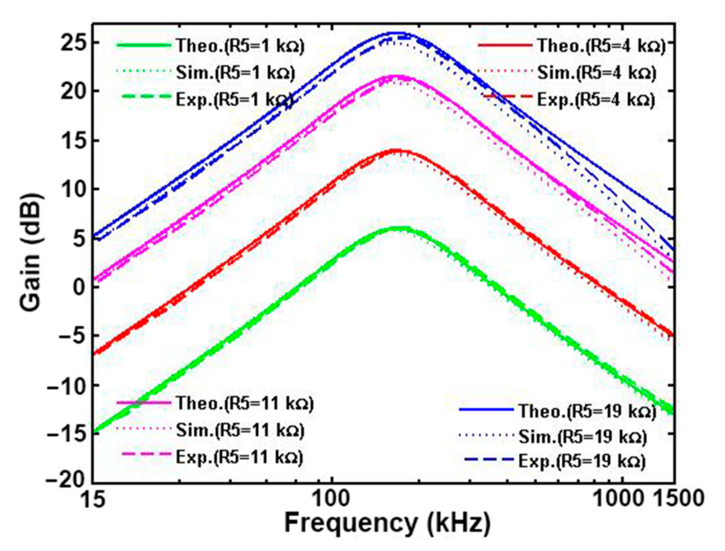
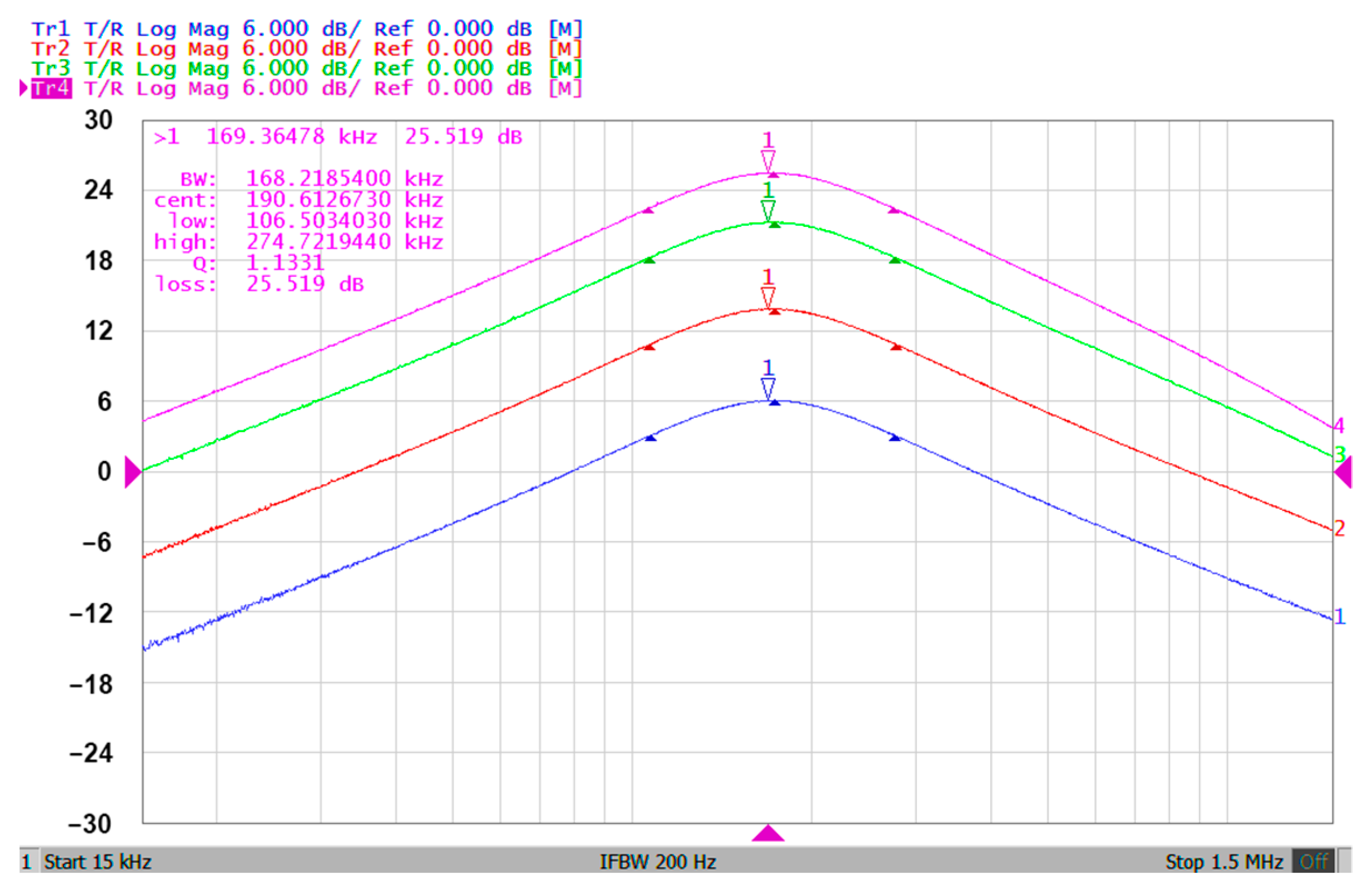
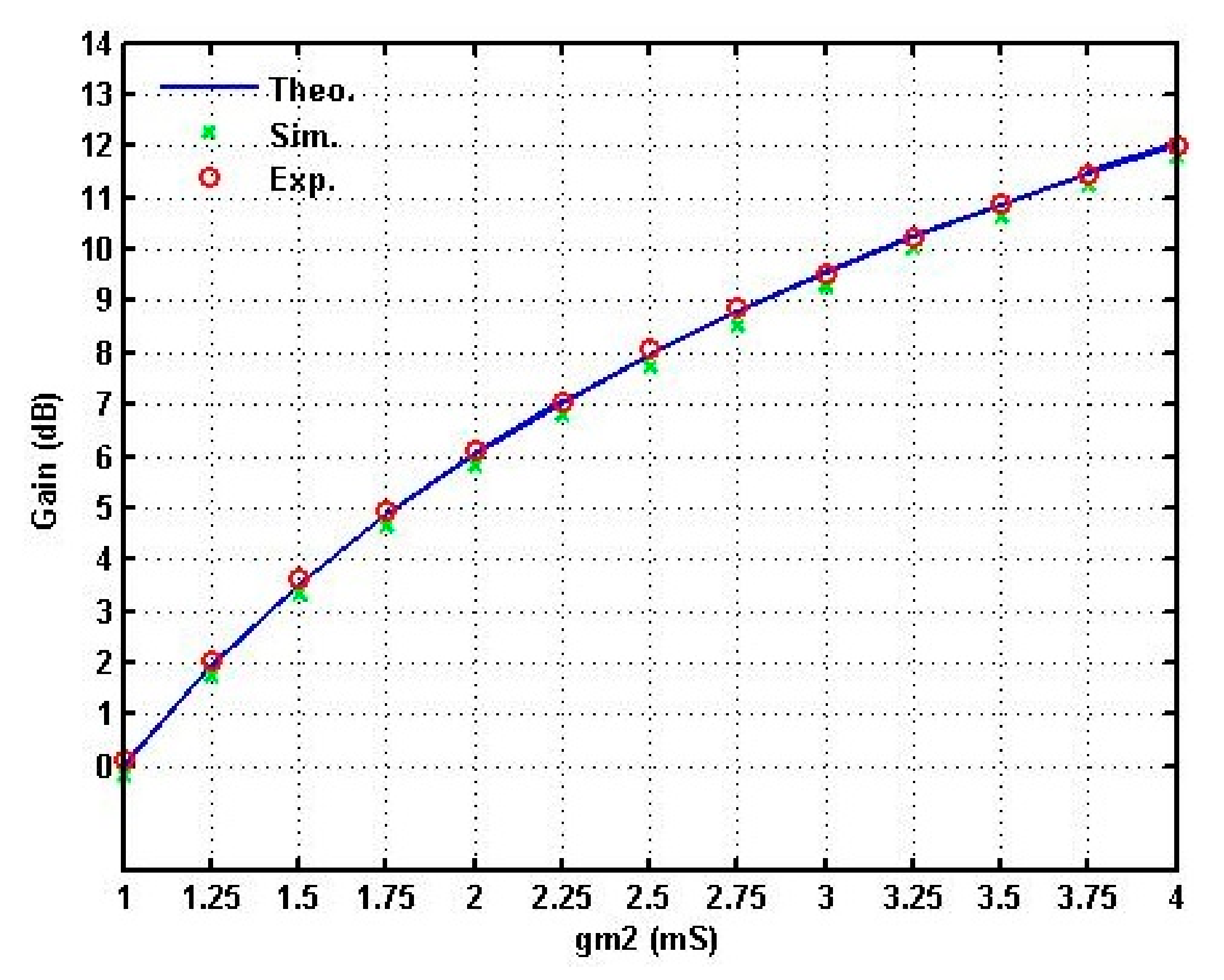
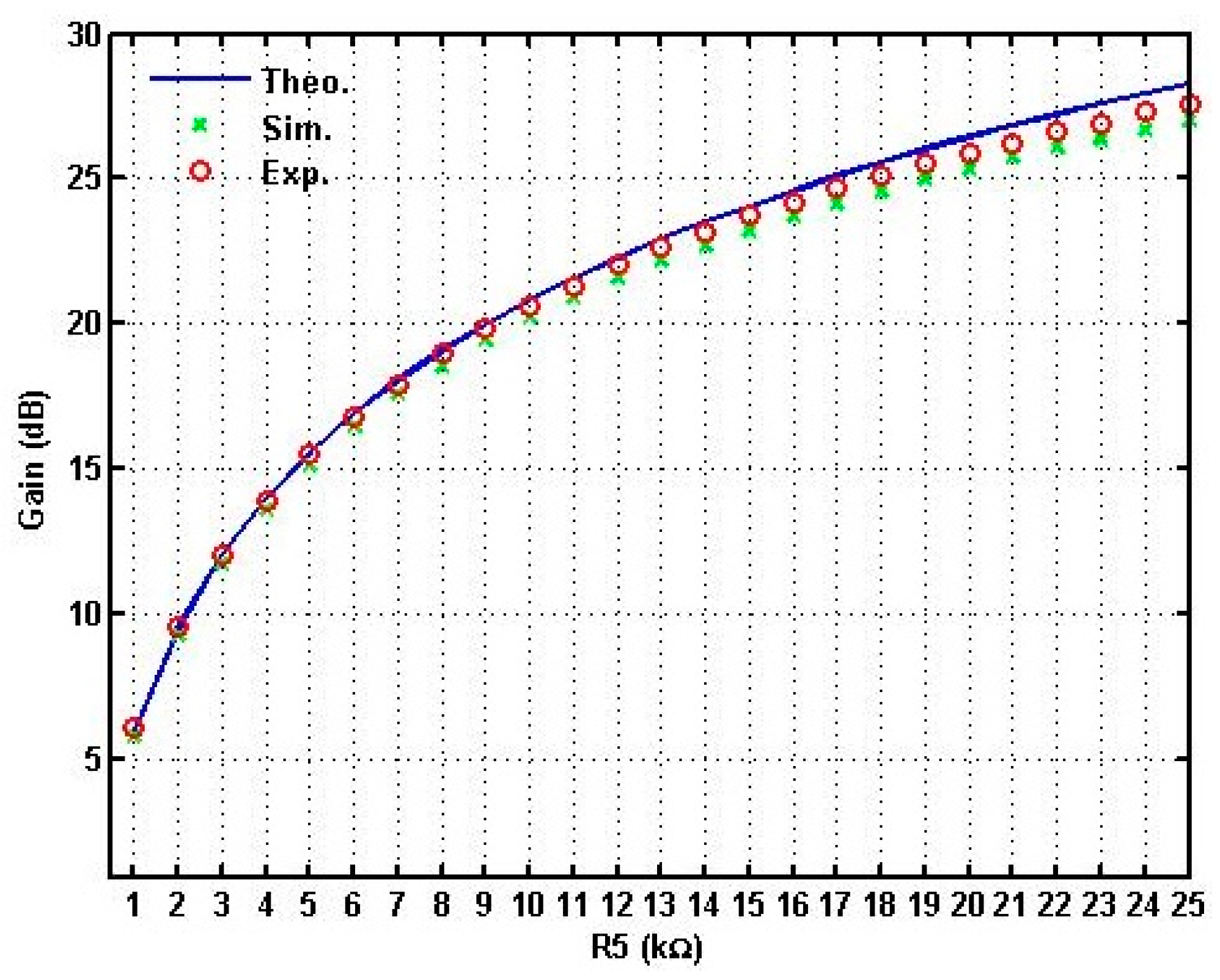
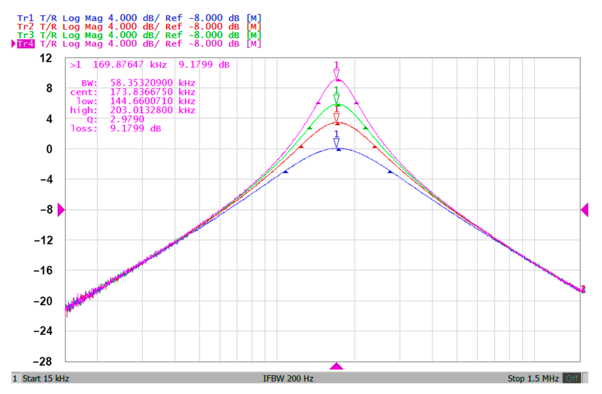
3.1. First Proposed Isomorphic Circuit Simulation and Experimental Results
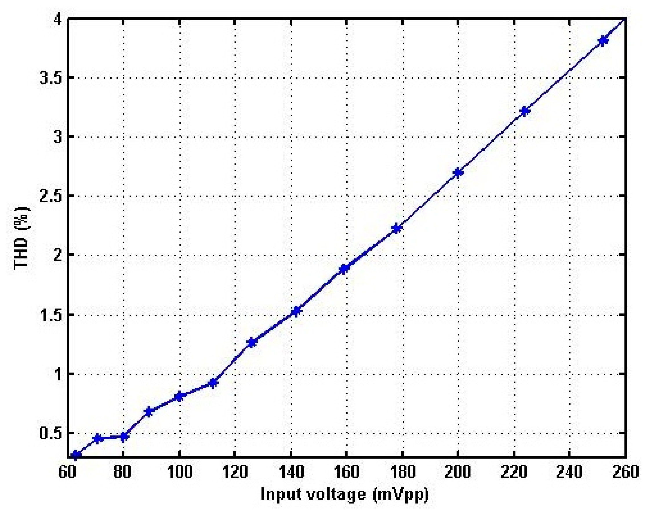
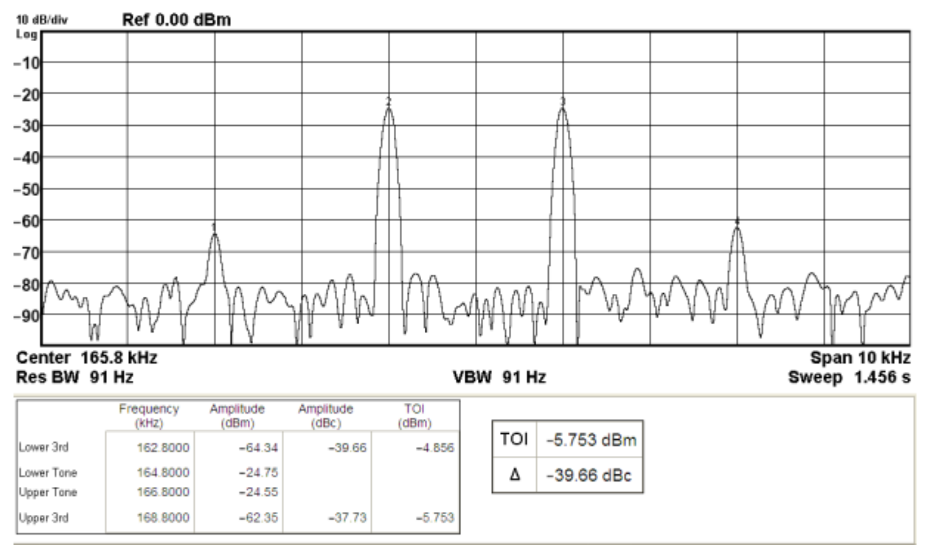
3.2. Second Proposed Isomorphic Circuit Simulation and Experimental Results
4. Concluding Remarks
Author Contributions
Funding
Institutional Review Board Statement
Informed Consent Statement
Data Availability Statement
Conflicts of Interest
References
- Olsak, M.; Vrba, K.; Matejicek, L. Electronically tunable high-order highpass filters with minimum of components. J. Electr. Eng. 2003, 54, 57–62. [Google Scholar]
- Siripongdee, S.; Jaikla, W. Electronically controllable grounded inductance simulators using single commercially available IC: LT1228. AEU-Int. J. Electron. Commun. 2017, 76, 1–10. [Google Scholar] [CrossRef]
- Siripongdee, S.; Jaikla, W. Universal filter using single commercially available IC: LT1228. In Proceedings of the 2016 the 3rd International Conference on Mechatronics and Mechanical Engineering, Kuala Lumpur, Malaysia, 28–30 November 2017; Volume 95, p. 14022. [Google Scholar]
- Rungsa, S.; Jantakun, A. Single commercially available IC: LT1228 based sinusoidal oscillator. Prz. Elektrotechniczny 2019, 95, 218–222. [Google Scholar] [CrossRef]
- Klungtong, S.; Thanapatay, D.; Jaikla, W. Three-input single-output voltage-mode multifunction filter with electronic controllability based on single commercially available IC. Act. Passiv. Electron. Compon. 2017, 2017, 5240751. [Google Scholar] [CrossRef]
- Chaichana, A.; Siripongdee, S.; Jaikla, W. Electronically adjustable voltage-mode first-order allpass filter using single commercially available IC. In Proceedings of the 2019 International Conference on Smart Materials Applications, Tokyo, Japan, 19–22 January 2019; p. 012009. [Google Scholar]
- Wai, M.P.P.; Chaichana, A.; Jaikla, W.; Siripongdee, S.; Suwanjan, P. One input voltage and three output voltage universal biquad filters with orthogonal tune of frequency and bandwidth. Int. J. Electr. Comput. Eng. 2021, 20, 2962–2973. [Google Scholar]
- Roongmuanpha, N.; Suesut, T.; Tangsrirat, W. Electronically tunable triple-input single-output voltage-mode biquadratic filter implemented with single integrated circuit package. Adv. Sci. Technol. Eng. Syst. J. 2021, 6, 1120–1127. [Google Scholar] [CrossRef]
- Wang, H.Y.; Tran, H.D.; Nguyen, Q.M.; Yin, L.T.; Liu, C.Y. Derivation of oscillators from biquadratic band pass filters using circuit transformations. Appl. Sci. 2014, 4, 482–492. [Google Scholar] [CrossRef]
- Tran, H.D.; Wang, H.Y.; Lin, M.C.; Nguyen, Q.M. Synthesis of cascadable DDCC-based universal filter using NAM. Appl. Sci. 2015, 5, 320–343. [Google Scholar] [CrossRef]
- Minaei, S.; Sayin, O.K.; Kuntman, H. A new CMOS electronically tunable current conveyor and its application to current-mode filters. IEEE Trans. Circuits Syst. I 2006, 53, 1448–1457. [Google Scholar] [CrossRef]
- Herencsar, N.; Koton, J.; Hanak, P. Universal voltage conveyor and its novel dual-output fully-cascadable VM APF application. Appl. Sci. 2017, 7, 307. [Google Scholar] [CrossRef]
- Sotner, R.; Jerabek, J.; Langhammer, L.; Dvorak, J. Design and analysis of CCII-based oscillator with amplitude stabilization employing optocouplers for linear voltage control of the output frequency. Electronics 2018, 7, 157. [Google Scholar] [CrossRef] [Green Version]
- Ullah, F.; Liu, Y.; Li, Z.; Wang, X.; Sarfraz, M.M.; Zhang, H. A bandwidth-enhanced differential LC-voltage controlled oscillator (LC-VCO) and superharmonic coupled quadrature VCO for K-band applications. Electronics 2018, 7, 127. [Google Scholar] [CrossRef] [Green Version]
- Safari, L.; Barile, G.; Ferri, G.; Stornelli, V. A new low-voltage low-power dual-mode VCII-based SIMO universal filter. Electronics 2019, 8, 765. [Google Scholar] [CrossRef] [Green Version]
- Márquez, A.; Pérez-Bailón, J.; Calvo, B.; Medrano, N.; Martínez, P.A. A CMOS self-contained quadrature signal generator for SoC impedance spectroscopy. Sensors 2018, 18, 1382. [Google Scholar] [CrossRef] [Green Version]
- Acosta, L.; Jimenez, M.; Carvajal, R.G.; Lopez-Martin, A.J.; Ramirez-Angulo, J. Highly linear tunable CMOS gm-C low-pass filter. IEEE Trans. Circuits Syst. I Regul. Pap. 2009, 56, 2145–2158. [Google Scholar] [CrossRef]
- Kumngern, M.; Aupithak, N.; Khateb, F.; Kulej, T. 0.5 V fifth-order butterworth low-pass filter using multiple-input OTA for ECG applications. Sensors 2020, 20, 7343. [Google Scholar] [CrossRef]
- Jaikla, W.; Khateb, F.; Kulej, T.; Pitaksuttayaprot, K. Universal filter based on compact CMOS structure of VDDDA. Sensors 2021, 21, 1683. [Google Scholar] [CrossRef]
- Psychalinos, C.; Kasimis, C.; Khateb, F. Multiple-input single-output universal biquad filter using single output operational transconductance amplifiers. AEU-Int. J. Electron. Commun. 2018, 93, 360–367. [Google Scholar] [CrossRef]
- Wang, S.F.; Chen, H.P.; Ku, Y.; Lin, Y.C. Versatile tunable voltage-mode biquadratic filter and its application in quadrature oscillator. Sensors 2019, 19, 2349. [Google Scholar] [CrossRef] [PubMed] [Green Version]
- Wang, S.F.; Chen, H.P.; Ku, Y.; Yang, C.M. Independently tunable voltage-mode OTA-C biquadratic filter with five inputs and three outputs and its fully-uncoupled quadrature sinusoidal oscillator application. AEU-Int. J. Electron. Commun. 2019, 100, 152822. [Google Scholar] [CrossRef]
- Jaikla, W.; Adhan, S.; Suwanjan, P.; Kumngern, M. Current/voltage controlled quadrature sinusoidal oscillators for phase sensitive detection using commercially available IC. Sensors 2020, 20, 1319. [Google Scholar] [CrossRef] [PubMed] [Green Version]
- Wang, S.F.; Chen, H.P.; Ku, Y.; Lee, C.L. Versatile voltage-mode biquadratic filter and quadrature oscillator using four OTAs and two grounded capacitors. Electronics 2020, 9, 1493. [Google Scholar] [CrossRef]
- LT1228–100 MHz Current Feedback Amplifier with DC Gain Control. Linear Technology Corporation Version Number D. 2012. Available online: http://www.linear.com/product/LT1228 (accessed on 1 October 2019).
- Koton, J.; Vrba, K.; Herencsar, N. Voltage-mode full-wave rectifier based on DXCCII. Analog Integr. Circuits Signal. Process. 2014, 81, 99–107. [Google Scholar] [CrossRef]
- Martin, R.S.; Tello, P.; Valencia, A.; Marzo, A. Experimental evaluation of distortion in amplitude modulation techniques for parametric loudspeakers. Appl. Sci. 2020, 10, 2070. [Google Scholar] [CrossRef] [Green Version]
- Alpaslan, H.; Yuce, E. DVCC+ based multifunction and universal filters with the high input impedance features. Analog Integr. Circuits Signal. Process. 2020, 103, 325–335. [Google Scholar] [CrossRef]


| Parameter | Figures 1 and 2 in [21] | Figures 1 and 4 in [22] | Figure 5 in [23] | First Proposed in This Work | Second Proposed in This Work |
|---|---|---|---|---|---|
| Number of active devices | 5 (OTA) | 5 (OTA) | 3 (LT1228) | 3 (LT1228) | 3 (LT1228) |
| Number of passive elements | 2 (2C) | 2 (2C) | 7 (2C, 5R) | 5 (2C, 3R) | 5 (2C, 3R) |
| Orthogonal tunability of ωo and Q | yes | yes | NA | yes | yes |
| High-input and low-output impedance of the filter | no | no | NA | yes | yes |
| Independent tunability of the filter amplitude | no | no | NA | yes | yes |
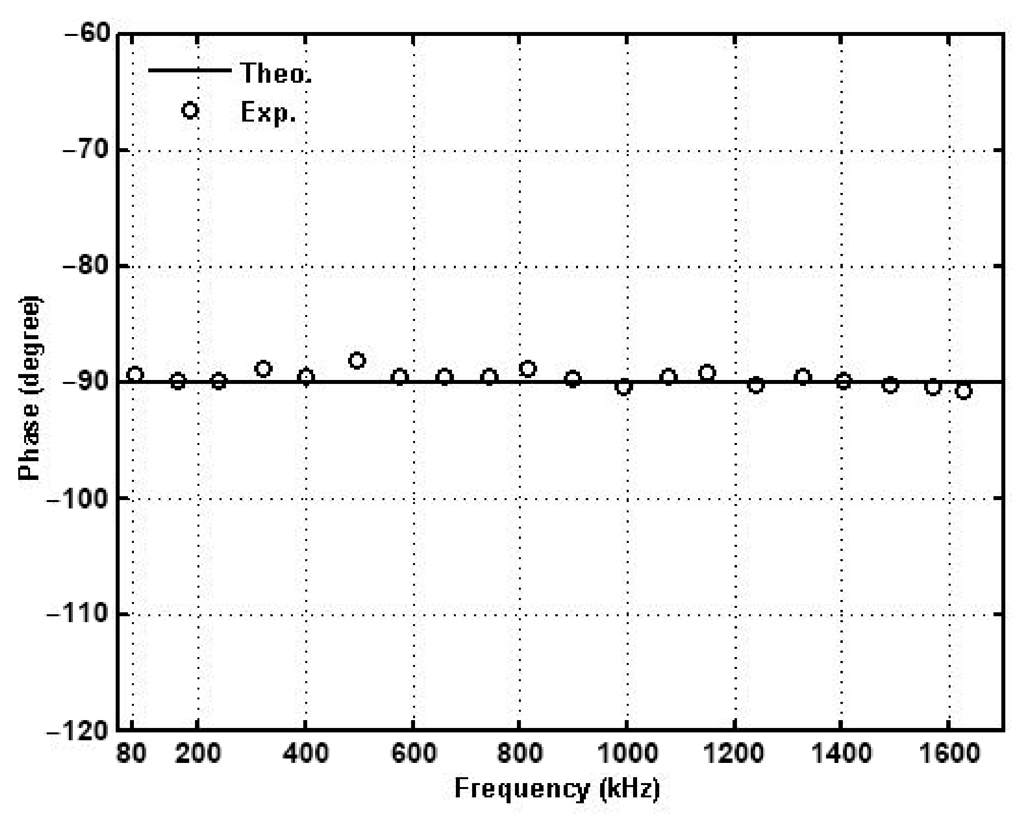
| Electronic and linear tune of oscillation frequency | no | yes | yes | yes | yes |
| Oscillator CO and FO with fully uncoupled electronic tuning law | no | yes | yes | yes | yes |
| Oscillator’s amplitude tunability | no | no | yes | yes | yes |
| Parameter | Figure 1 in [21] | Figure 1 in [22] | First Proposed in This Work | Second Proposed in This Work |
|---|---|---|---|---|
| Supply voltage | ±2 V | ±15 V | ±5 V | ±5 V |
| Measured power dissipation | 0.14 W | 1.2 W | 0.22 W | 0.22 W |
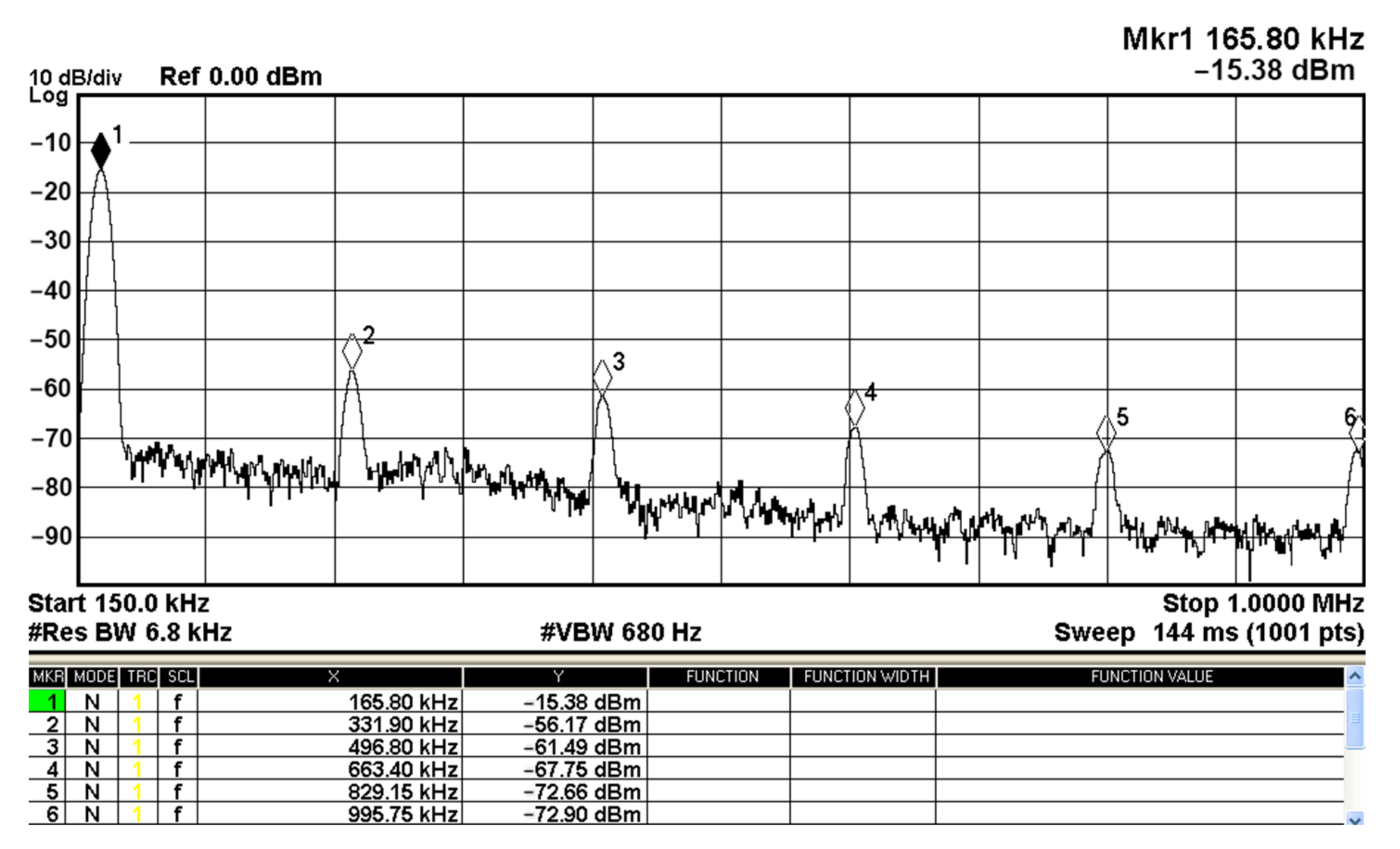
| Designed center frequency | 159.16 kHz | 217 kHz | 165.8 kHz | 165.8 kHz |
| Measured maximum operating voltage gain | 0 dB | 0 dB | 27.86 dB | 27.58 dB |
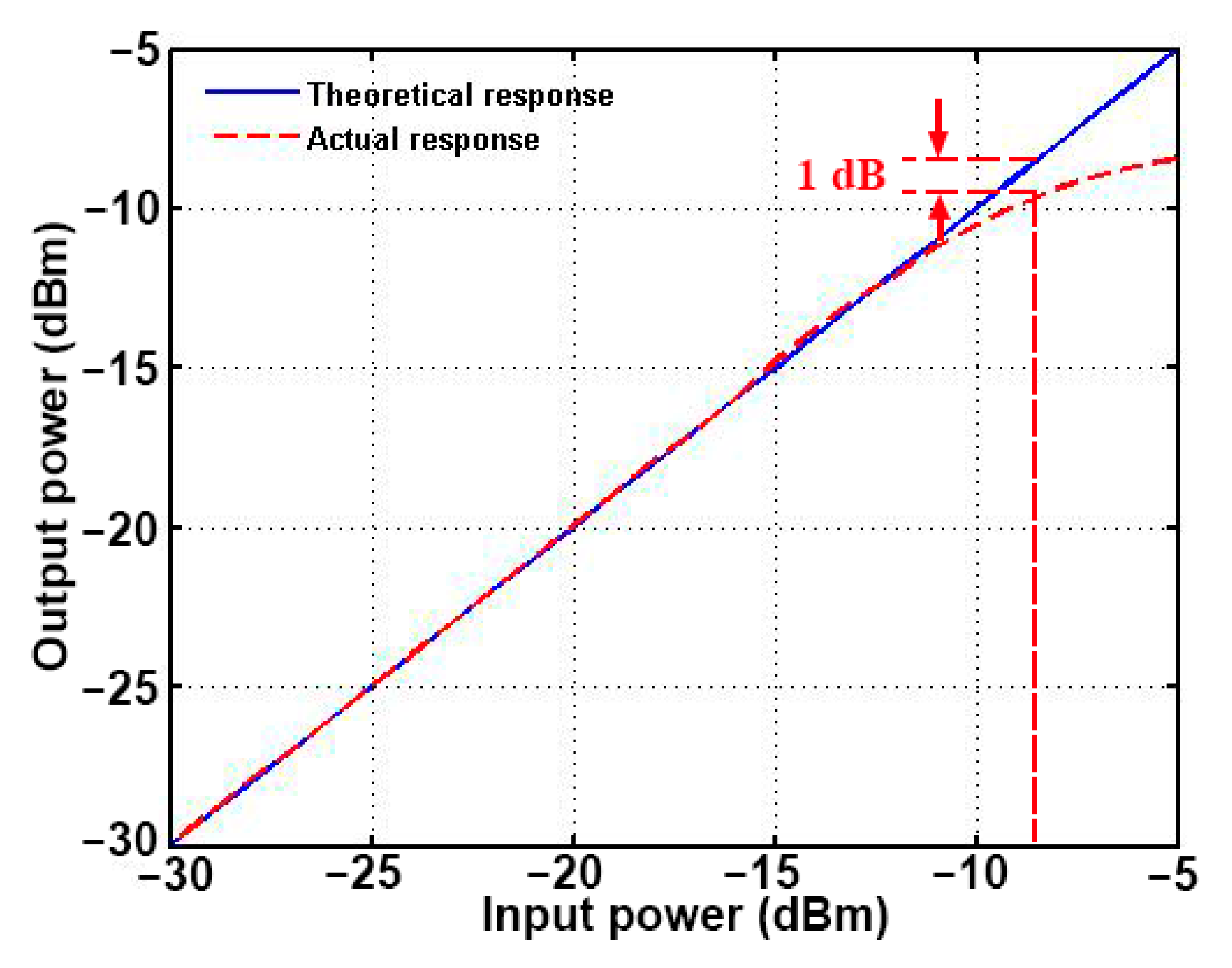
| Measured output P1dB (dBm) | −14.6 | NT | −11.4 | −9.77 |
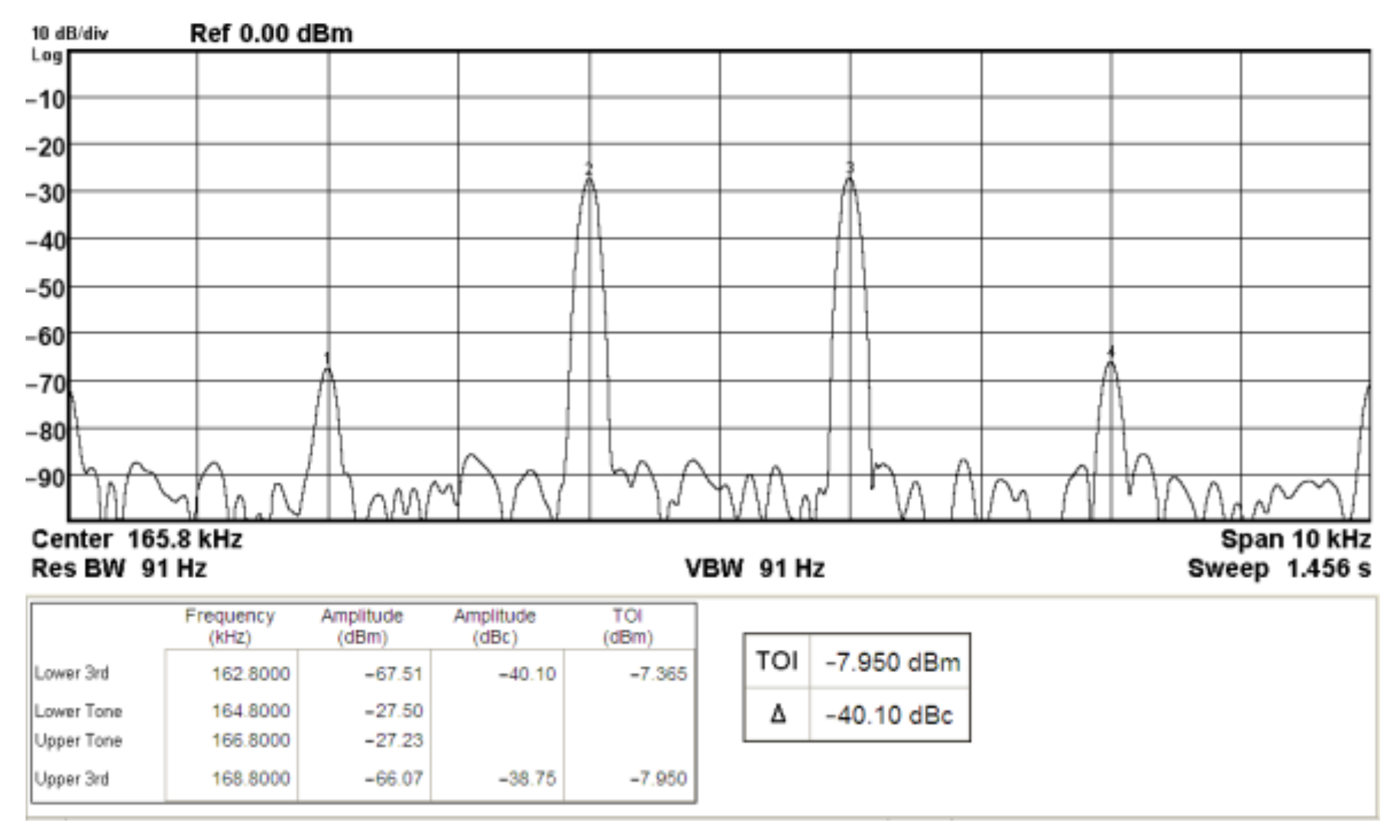
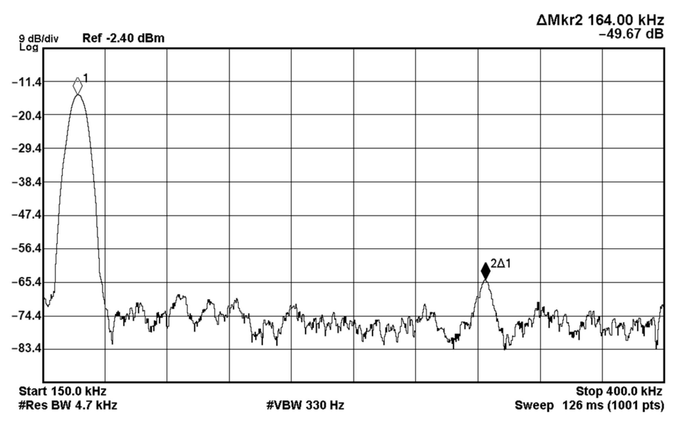
| Measured IMD3 (dBc) | −42.86 | −31.16 | −40.1 | −39.66 |
| Measured third-order intercept point (dBm) | −5.47 | NT | −7.95 | −5.753 |
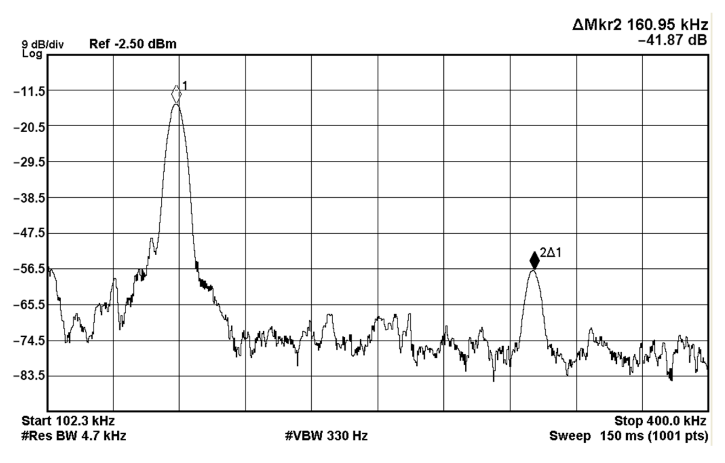
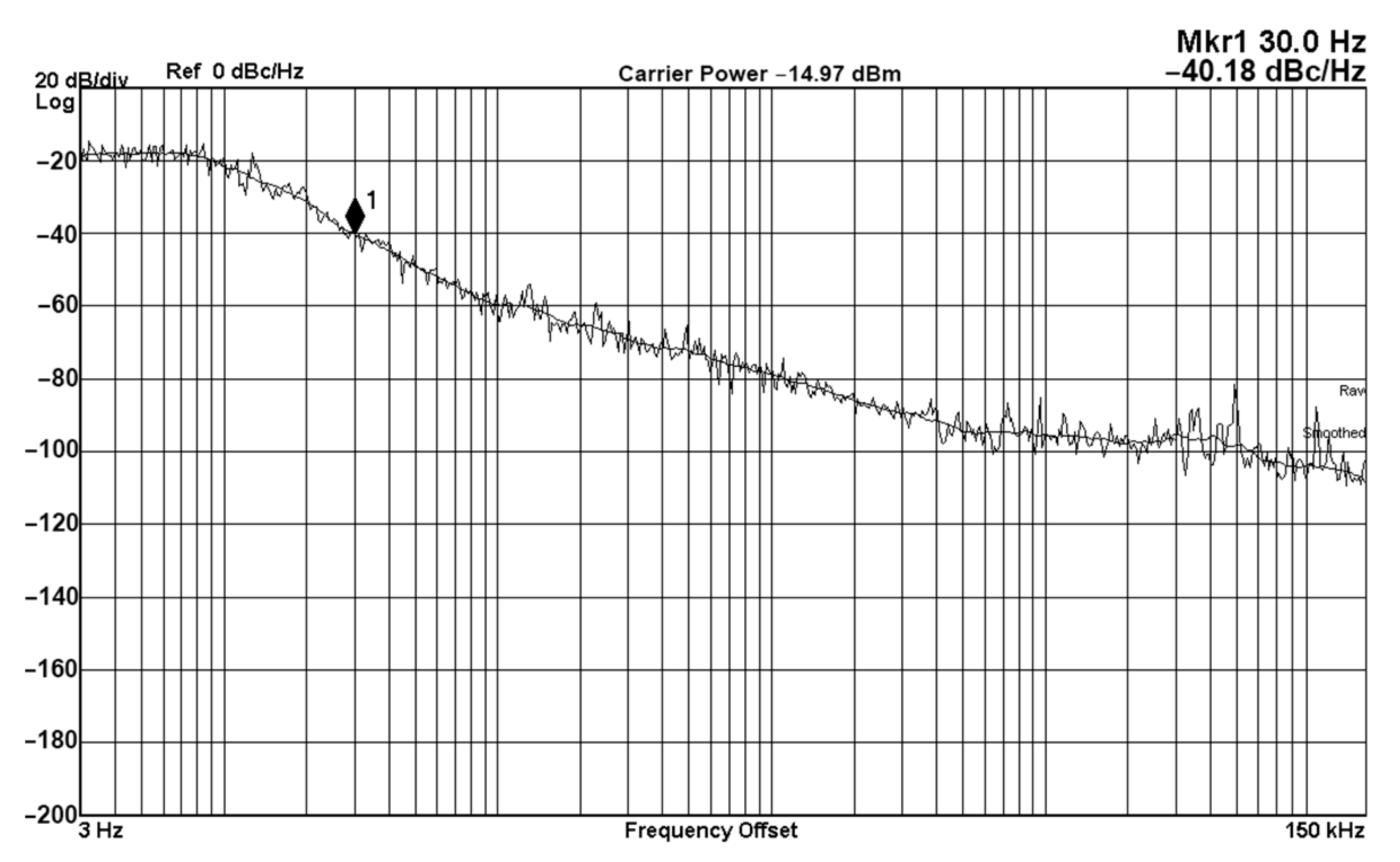
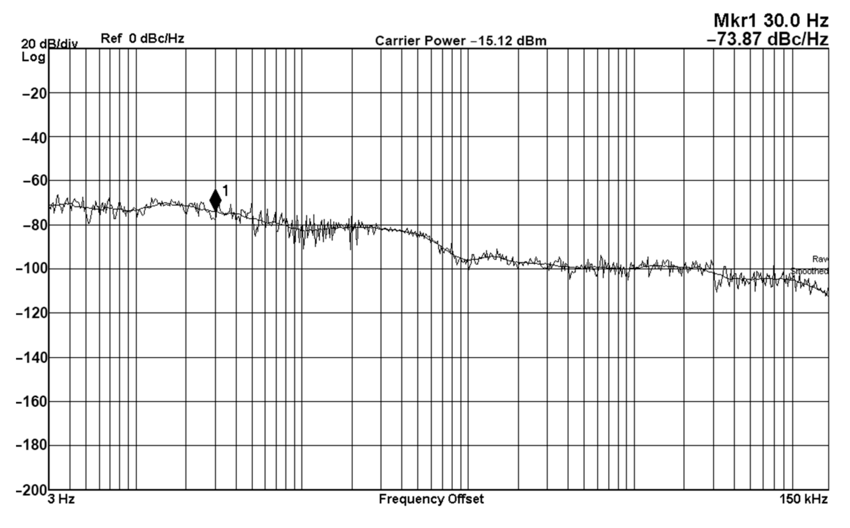
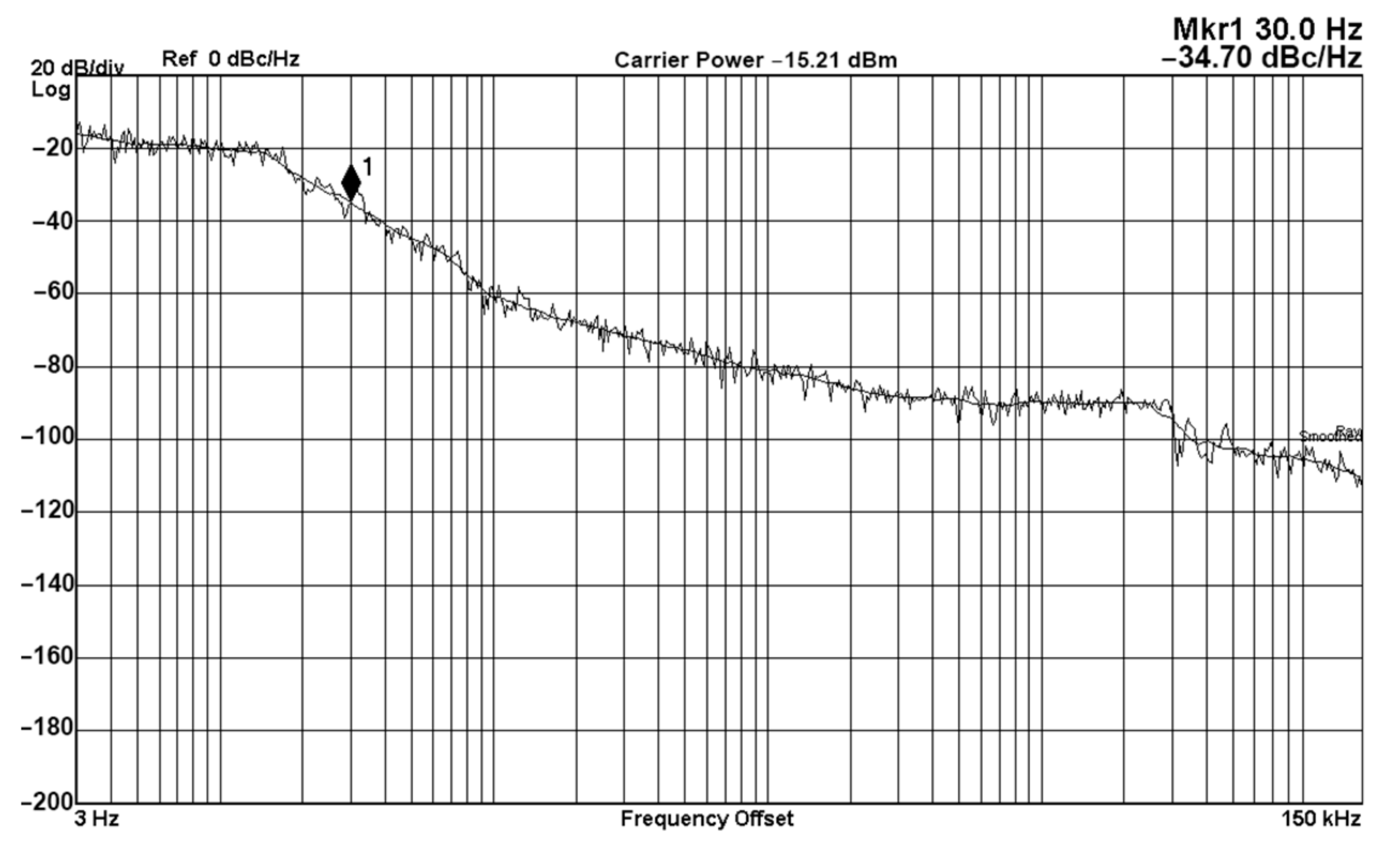
| Measured phase noise (dBc/Hz) | NT | NT | −83.86 | −73.87 |
| Figure of merit | NT | NT | 3.07 × 10⁶ | 3.08 × 10⁶ |
| Parameter | Figure 2 in [21] | Figure 4 in [22] | Figure 5 in [23] | First Proposed in This Work | Second Proposed in This Work |
|---|---|---|---|---|---|
| Supply voltage | ±15 V | ±15 V | ±5 V | ±5 V | ±5 V |
| Measured power dissipation | NT | 1.2 W | 1.98 W | 0.22 W | 0.22 W |
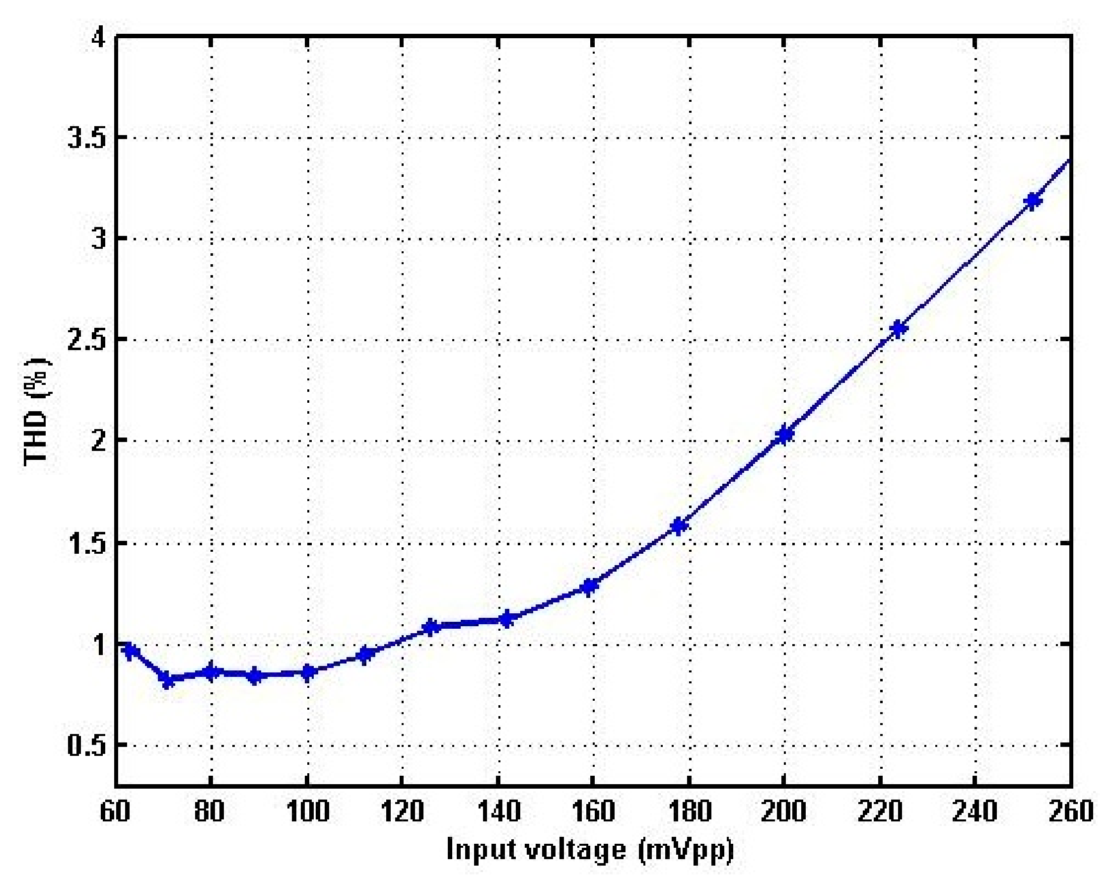
| Measured total harmonic distortion (%) | NT | NT | <1.26 | 0.81 | 0.33 |
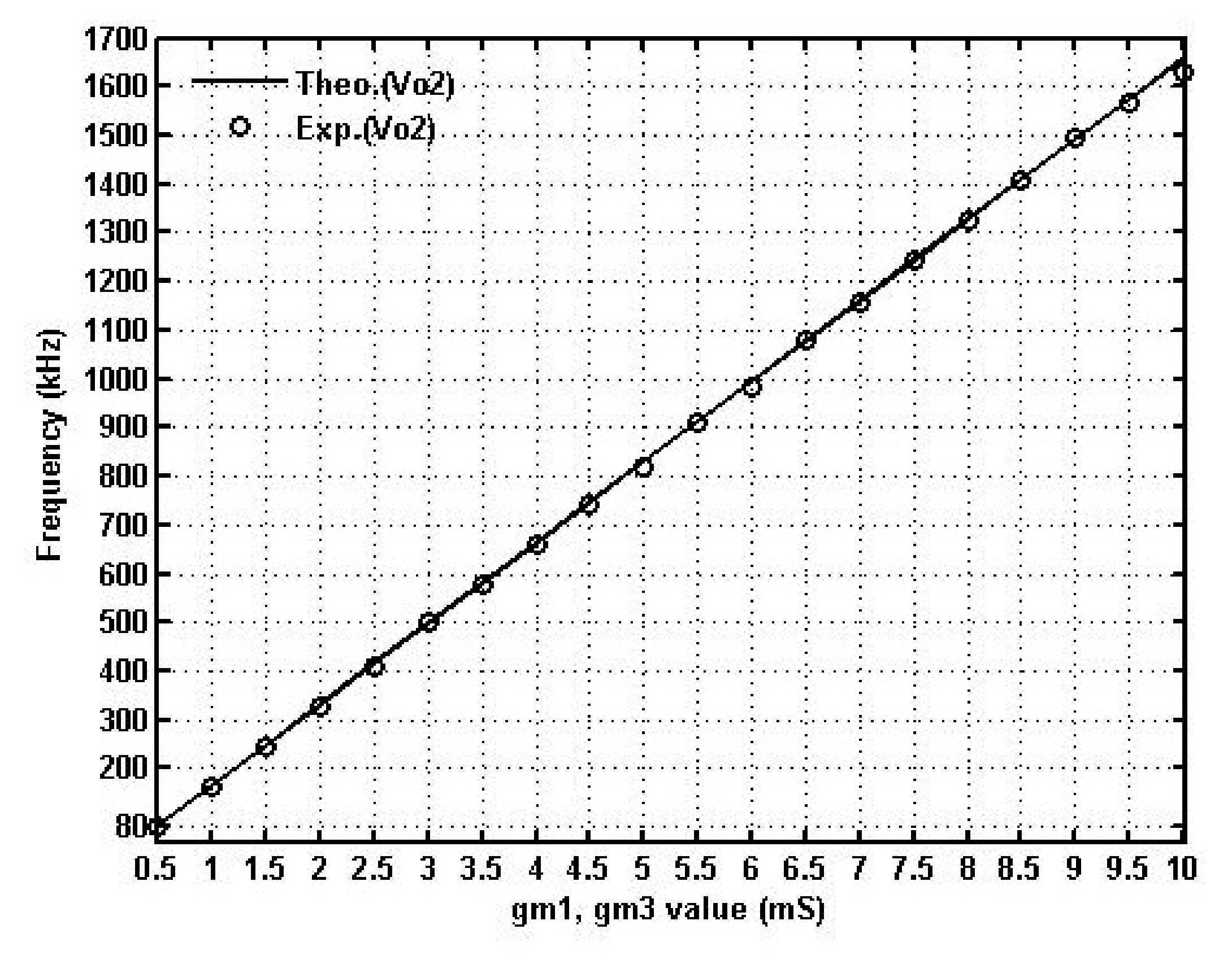
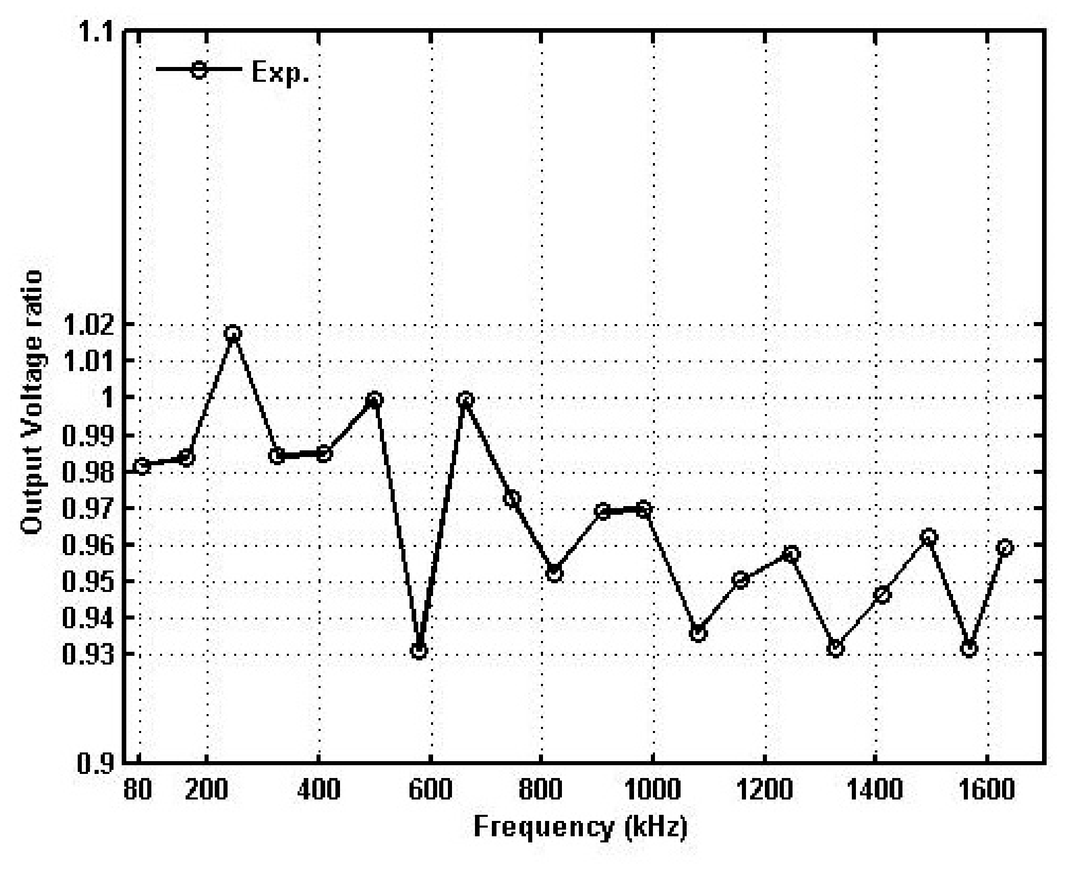
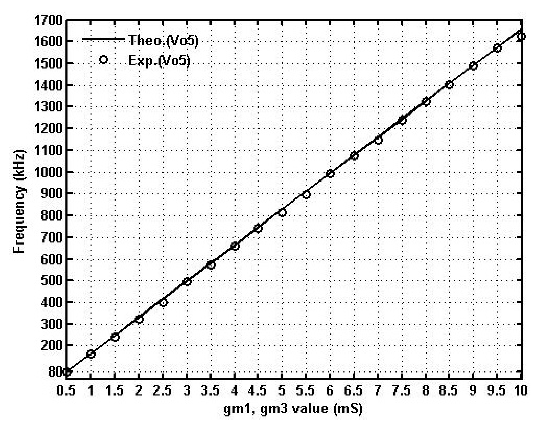
| Measured frequency tunable range (kHz) | NT | 150.1~2653 | 8.21~1117.51 | 82.15~1629 | 80.83~1626 |
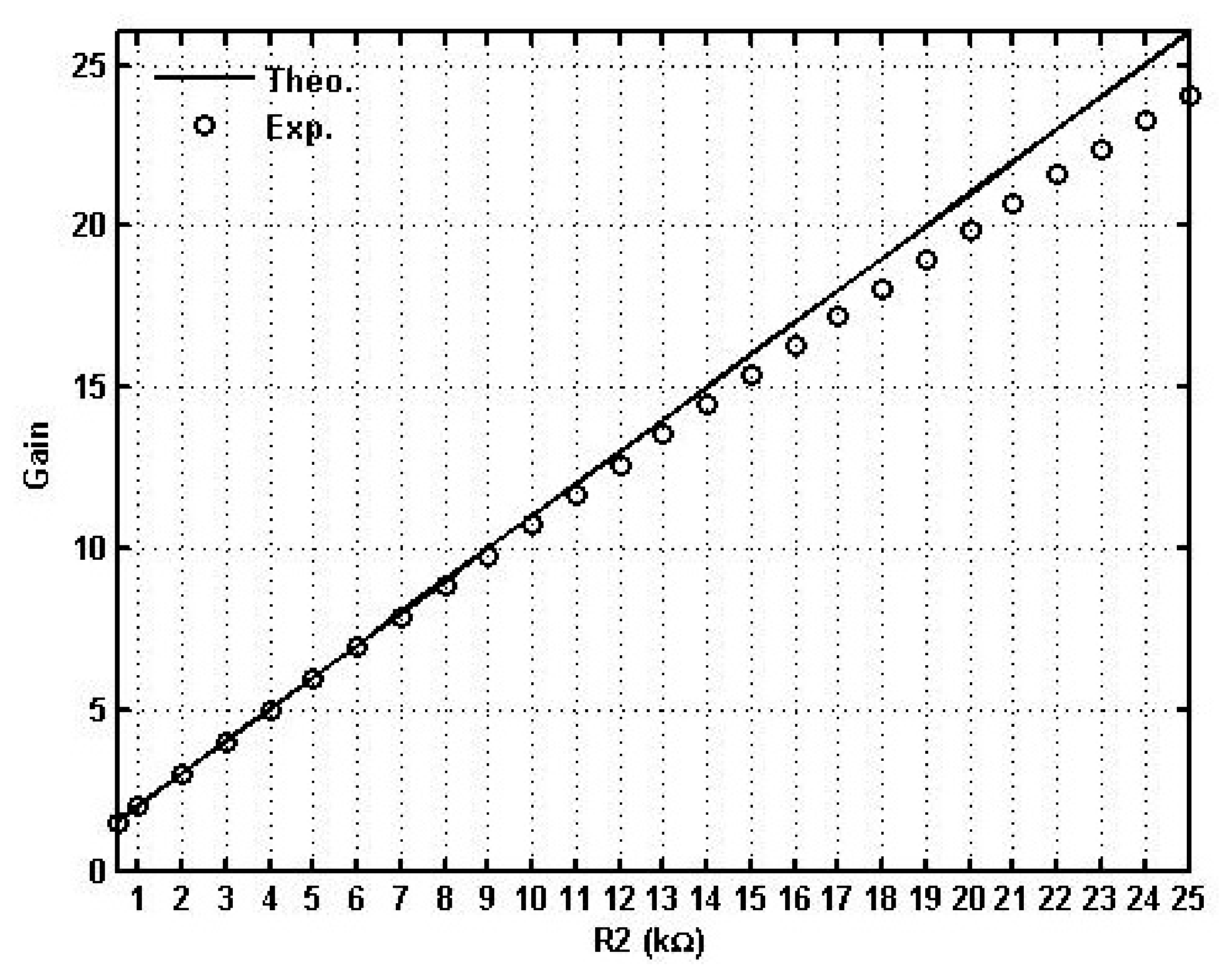
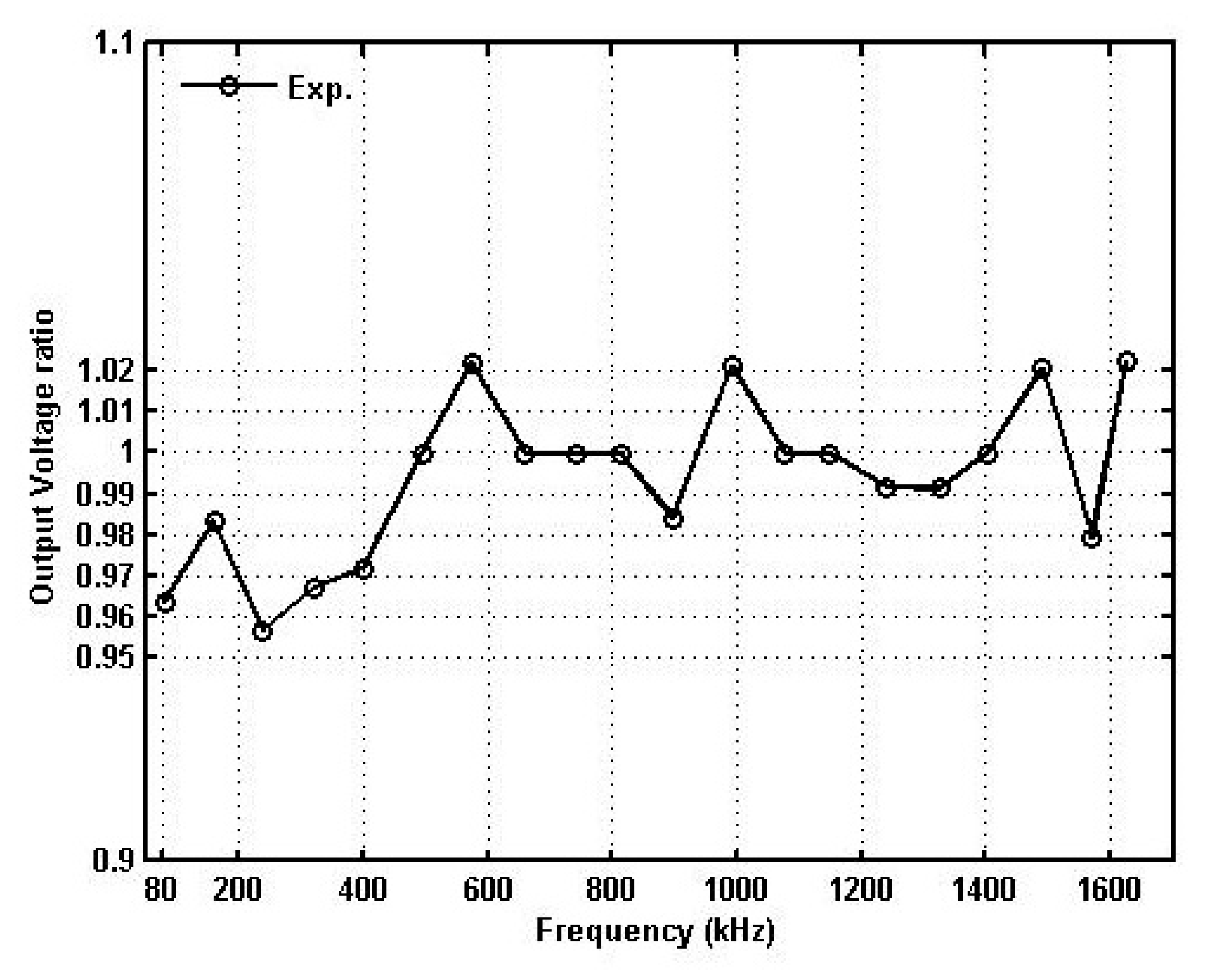
| Measured amplitude tunability range | NA | NA | 1.97~15.92 | 1.51~24.05 | 1.51~24.03 |
| Measured phase noise (dBc/Hz) | NT | −73.23 (@ 1000 Hz) | NT | −40.18 (@ 30 Hz) | −34.7 (@ 30 Hz) |
| Non-Inverting Bandpass Filter Factor | |
|---|---|
| Supply voltage (V) | ±5 |
| Power dissipation (W, measurement) | 0.22 |
| Central frequency (kHz, design/measurement) | 165.8/161.7 |
| Maximum operating voltage gain (dB, design/measurement) | 28.3/27.86 |
| Measured total harmonic distortion at Vin = 120 mVPP (%) | 1.08 |
| Measured output 1-dB compression point (dBm) | −11.4 |
| Measured third-order intermodulation distortion at 63 mVPP (dBc) | −40.1 |
| Measured third-order intercept point (dBm) | −7.95 |
| Measured phase noise at 30 Hz (dBc/Hz) | −83.86 |
| Measured spurious-free dynamic range (dB) | 40.79 |
| Figure of merit | 3.07 × 10⁶ |
| Fully Uncoupled Quadrature Oscillator Factor | |
| Supply voltage (V) | ±5 |
| Power dissipation (W, measurement) | 0.22 |
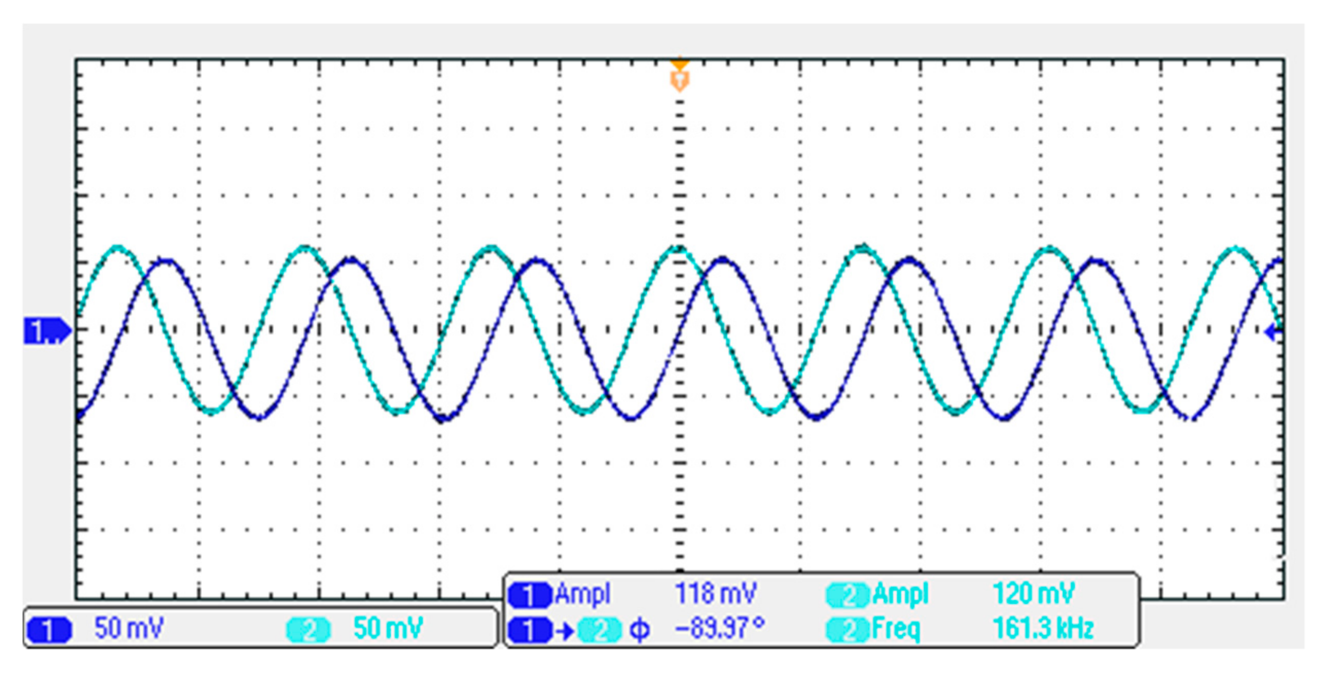
| Number of sinusoidal voltage output used | 3 |
| Oscillation frequency (kHz, design/measurement) | 165.8/162.3 |
| Measured total harmonic distortion (%) | 0.81 |
| Measured phase noise at 30 Hz (dBc/Hz) | −40.18 |
| Measured operating oscillation frequency range (kHz) | 82.15~1629 |
| Measured operating amplitude control range | 1.51~24.05 |
| Non-Inverting Bandpass Filter Factor | |
|---|---|
| Supply voltage (V) | ±5 |
| Power dissipation (W, measurement) | 0.22 |
| Central frequency (kHz, design/measurement) | 165.8/165.8 |
| Maximum operating voltage gain (dB, design/measurement) | 28.3/27.58 |
| Measured total harmonic distortion@ Vin = 120 mVPP (%) | 1.12 |
| Measured output 1-dB compression point (dBm) | −9.77 |
| Measured third-order intermodulation distortion at 63 mVPP (dBc) | −39.66 |
| Measured third-order intercept point (dBm) | −5.753 |
| Measured phase noise at 30 Hz (dBc/Hz) | −73.87 |
| Measured spurious-free dynamic range (dB) | 40.86 |
| Figure of merit | 3.08 × 10⁶ |
| Fully Uncoupled Quadrature Oscillator Factor | |
| Supply voltage (V) | ±5 |
| Power dissipation (W, measurement) | 0.22 |
| Number of sinusoidal voltage output used | 3 |
| Oscillation frequency (kHz, design/measurement) | 165.8/161.3 |
| Measured total harmonic distortion (%) | 0.33 |
| Measured phase noise at 30 Hz (dBc/Hz) | −34.7 |
| Measured operating oscillation frequency range (kHz) | 80.83~1626 |
| Measured operating amplitude control range | 1.51~24.03 |
Publisher’s Note: MDPI stays neutral with regard to jurisdictional claims in published maps and institutional affiliations. |
© 2021 by the authors. Licensee MDPI, Basel, Switzerland. This article is an open access article distributed under the terms and conditions of the Creative Commons Attribution (CC BY) license (https://creativecommons.org/licenses/by/4.0/).
Share and Cite
Wang, S.-F.; Chen, H.-P.; Ku, Y.; Chen, W.-Y. Isomorphic Circuits of Independent Amplitude Tunable Voltage-Mode Bandpass Filters and Quadrature Sinusoidal Oscillators. Appl. Sci. 2021, 11, 7431. https://doi.org/10.3390/app11167431
Wang S-F, Chen H-P, Ku Y, Chen W-Y. Isomorphic Circuits of Independent Amplitude Tunable Voltage-Mode Bandpass Filters and Quadrature Sinusoidal Oscillators. Applied Sciences. 2021; 11(16):7431. https://doi.org/10.3390/app11167431
Chicago/Turabian StyleWang, San-Fu, Hua-Pin Chen, Yitsen Ku, and Wei-Yuan Chen. 2021. "Isomorphic Circuits of Independent Amplitude Tunable Voltage-Mode Bandpass Filters and Quadrature Sinusoidal Oscillators" Applied Sciences 11, no. 16: 7431. https://doi.org/10.3390/app11167431
APA StyleWang, S.-F., Chen, H.-P., Ku, Y., & Chen, W.-Y. (2021). Isomorphic Circuits of Independent Amplitude Tunable Voltage-Mode Bandpass Filters and Quadrature Sinusoidal Oscillators. Applied Sciences, 11(16), 7431. https://doi.org/10.3390/app11167431