
Integrated Electromagnetic-Thermal Approach to Simulate a GaN-Based Monolithic Half-Bridge for Automotive DC-DC Converter

 , ,
, ,
Abstract
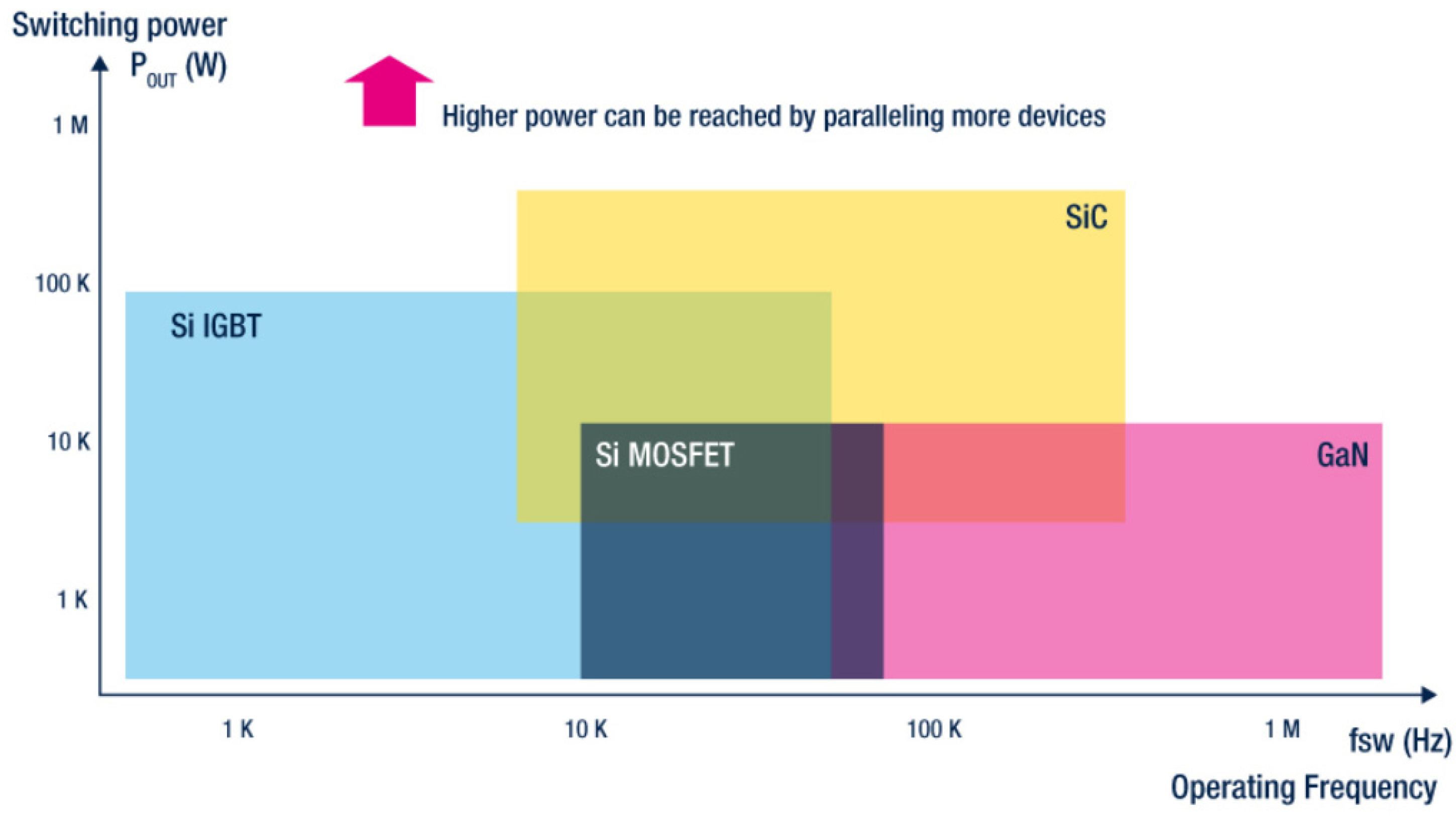
:1. Introduction
2. Package Description and Integrated Simulation Methodology
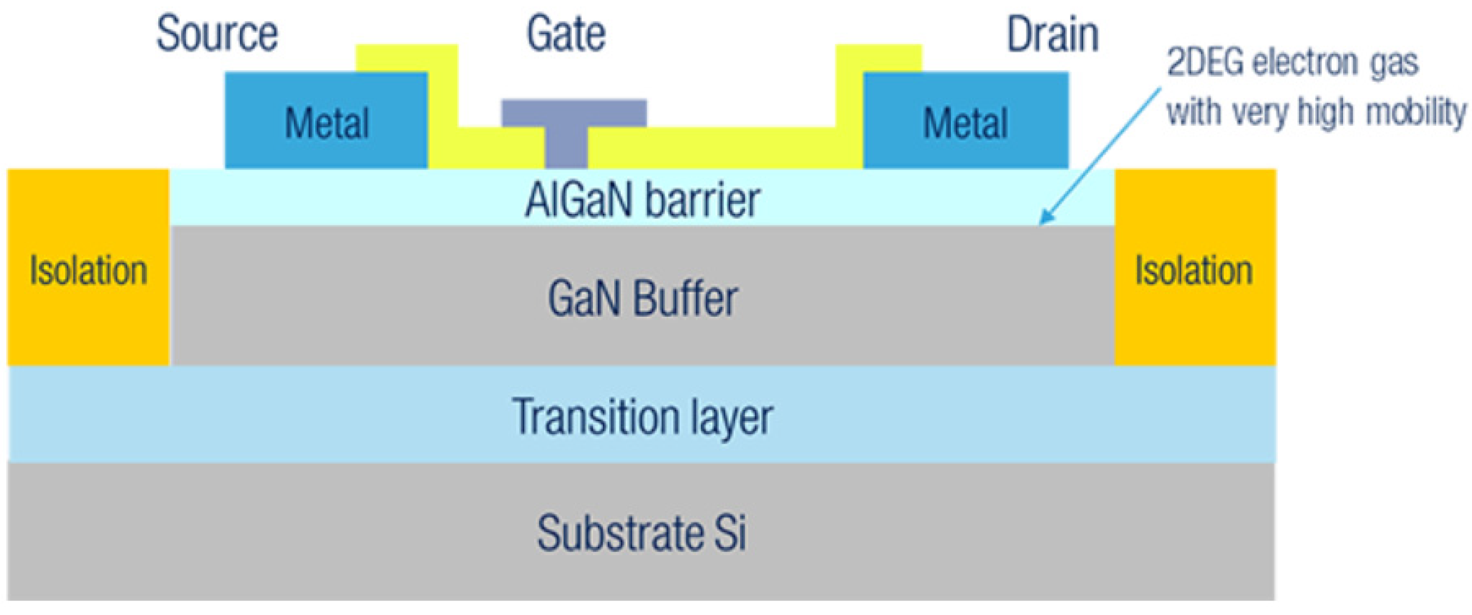
2.1. Integrated GaN Package Description
2.2. Simulation Methodology Outline
3. Electromagnetic Simulation
3.1. Q3D Extractor Theory
3.2. Electromagnetic Simulation Setup
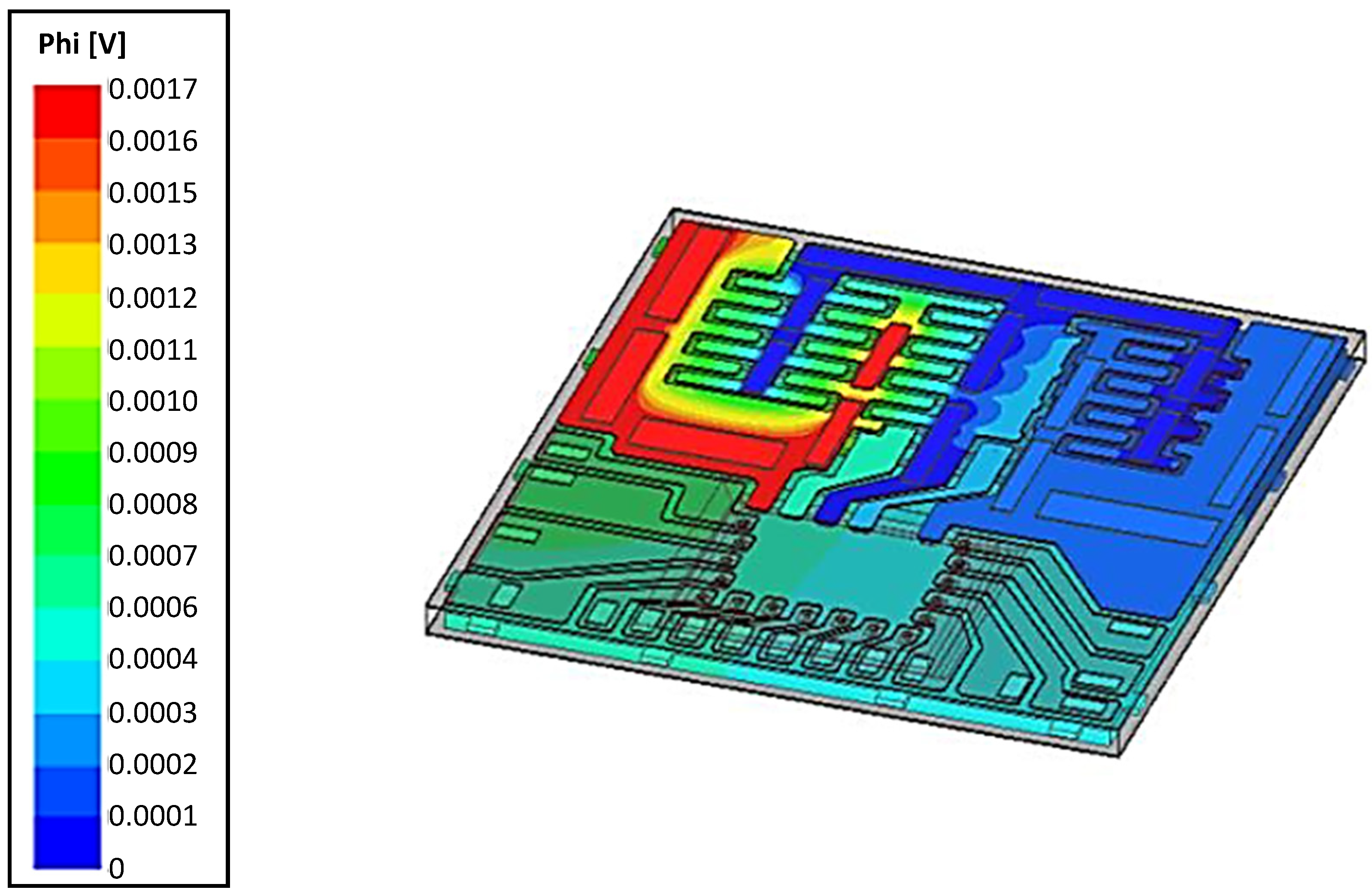
3.3. Electromagnetic Simulation Results
4. Thermal Simulation
4.1. Thermal Resistance Calibration and Model Semplification
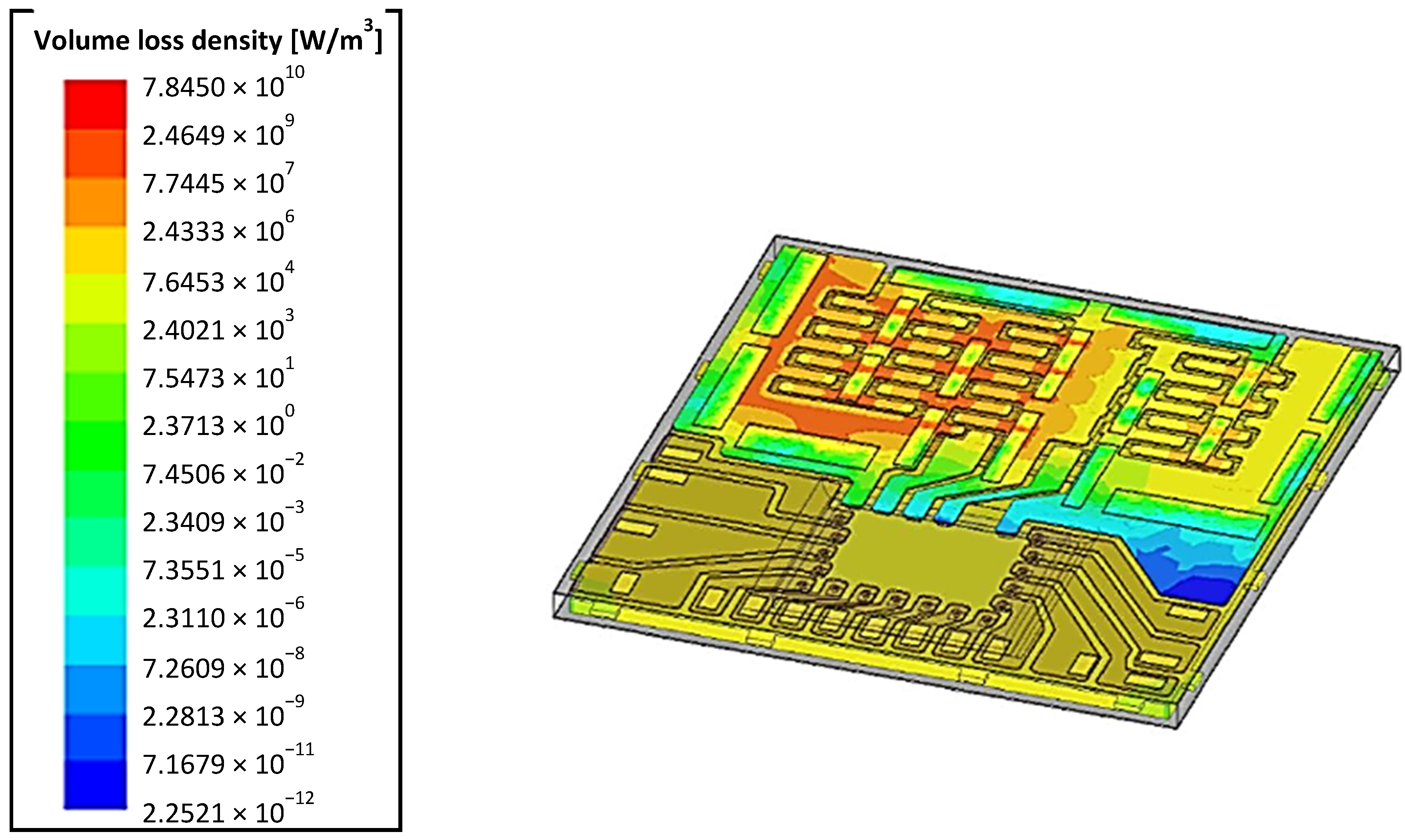
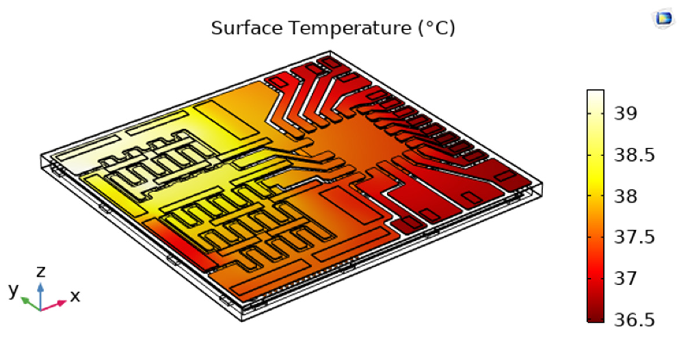
4.2. Thermal Simulation Results
5. Conclusions
Author Contributions
Funding
Institutional Review Board Statement
Informed Consent Statement
Data Availability Statement
Conflicts of Interest
References
- Li, S.; Lu, S.; Mi, C.C. Revolution of electric vehicle charging technologies accelerated by wide bandgap devices. Proc. IEEE 2021, 109, 985–1003. [Google Scholar] [CrossRef]
- Keshmiri, N.; Wang, D.; Agrawal, B.; Hou, R.; Emadi, A. Current status and future trends of GaN HEMTs in electrified transportation. IEEE Access 2020, 8, 70553–70571. [Google Scholar] [CrossRef]
- Santopa, M.; Russo, S.; Torrisi, M.; Renna, M.; Sitta, A.; Calabretta, M. Fast transient thermomechanical stress to set a pressure-assisted sintering process. In Proceedings of the 2019 15th Conference on Ph.D. Research in Microelectronics and Electronics (PRIME), Lausanne, Switzerland, 15–18 July 2019; pp. 61–64. [Google Scholar]
- Millan, J.; Godignon, P.; Perpina, X.; Perez-Tomas, A.; Rebollo, J. A survey of wide bandgap power semiconductor devices. IEEE Trans. Power Electron. 2014, 29, 2155–2163. [Google Scholar] [CrossRef]
- Pellitteri, F.; Busacca, A.; Martorana, C.; Miceli, R.; Stivala, S.; Messina, A.A.; Calabretta, M.; Vinciguerra, V. Power losses comparison between silicon carbide and silicon devices for an isolated DC-DC converter. In Proceedings of the 2021 IEEE 15th International Conference on Compatibility, Power Electronics and Power Engineering (CPE-POWERENG), Florence, Italy, 14–16 July 2021. [Google Scholar]
- Jiya, I.N.; Gouws, R. Overview of power electronic switches: A summary of the past, state-of-the-art and illumination of the future. Micromachines 2020, 11, 1116. [Google Scholar] [CrossRef] [PubMed]
- Coffa, S.; Saggio, M.; Patti, A. SiC- and GaN-based power devices: Technologies, products and applications. In Proceedings of the 2015 IEEE International Electron Devices Meeting (IEDM), Washington, DC, USA, 11–15 December 2015; pp. 16.8.1–16.8.5. [Google Scholar]
- Knight, S.; Mock, A.; Korlacki, R.; Darakchieva, V.; Monemar, B.; Kumagai, Y.; Goto, K.; Higashiwaki, M.; Schubert, M. Electron effective mass in Sn-doped monoclinic single crystal β-gallium oxide determined by mid-infrared optical hall effect. Appl. Phys. Lett. 2018, 112, 012103. [Google Scholar] [CrossRef] [Green Version]
- Wang, T.; Li, W.; Ni, C.; Janotti, A. Band gap and band offset of Ga2O3 and (AlxGa1 − x)2O3 Alloys. Phys. Rev. Appl. 2018, 10, 011003. [Google Scholar] [CrossRef] [Green Version]
- Liu, X.; Sammarco, C.; Zeng, G.; Guo, D.; Tang, W.; Tan, C.-K. Investigations of monoclinic- and orthorhombic-based (BxGa1 − x)2O3 Alloys. Appl. Phys. Lett. 2020, 117, 012104. [Google Scholar] [CrossRef]
- Zhang, H.; Yuan, L.; Tang, X.; Hu, J.; Sun, J.; Zhang, Y.; Zhang, Y.; Jia, R. Progress of ultra-wide bandgap Ga2O3 semiconductor materials in power MOSFETs. IEEE Trans. Power Electron. 2020, 35, 5157–5179. [Google Scholar] [CrossRef]
- Jones, E.A.; Wang, F.F.; Costinett, D. Review of commercial GaN power devices and GaN-based converter design challenges. IEEE J. Emerg. Sel. Top. Power Electron. 2016, 4, 707–719. [Google Scholar] [CrossRef]
- Amano, H.; Baines, Y.; Beam, E.; Borga, M.; Bouchet, T.; Chalker, P.R.; Charles, M.; Chen, K.J.; Chowdhury, N.; Chu, R.; et al. The 2018 GaN power electronics roadmap. J. Phys. D Appl. Phys. 2018, 51, 163001. [Google Scholar] [CrossRef]
- Zeng, F.; An, J.X.; Zhou, G.; Li, W.; Wang, H.; Duan, T.; Jiang, L.; Yu, H. A comprehensive review of recent progress on GaN high electron mobility transistors: Devices, fabrication and reliability. Electronics 2018, 7, 377. [Google Scholar] [CrossRef] [Green Version]
- Dalla Vecchia, M.; Ravyts, S.; Van den Broeck, G.; Driesen, J. Gallium-nitride semiconductor technology and its practical design challenges in power electronics applications: An overview. Energies 2019, 12, 2663. [Google Scholar] [CrossRef] [Green Version]
- Ma, C.-T.; Gu, Z.-H. Review of GaN HEMT applications in power converters over 500 W. Electronics 2019, 8, 1401. [Google Scholar] [CrossRef] [Green Version]
- Roccaforte, F.; Greco, G.; Fiorenza, P.; Iucolano, F. An overview of normally-Off GaN-based high electron mobility transistors. Materials 2019, 12, 1599. [Google Scholar] [CrossRef] [PubMed] [Green Version]
- Chen, K.J.; Haberlen, O.; Lidow, A.; Tsai, C.L.; Ueda, T.; Uemoto, Y.; Wu, Y. GaN-on-Si power technology: Devices and applications. IEEE Trans. Electron. Devices 2017, 64, 779–795. [Google Scholar] [CrossRef]
- Ding, X.; Zhou, Y.; Cheng, J. A review of gallium nitride power device and its applications in motor drive. Trans. Electr. Mach. Syst. 2019, 3, 54–64. [Google Scholar] [CrossRef]
- Gareau, J.; Hou, R.; Emadi, A. Review of loss distribution, analysis, and measurement techniques for GaN HEMTs. IEEE Trans. Power Electron. 2020, 35, 7405–7418. [Google Scholar] [CrossRef]
- STMicroelectronics. GaN. Available online: https://www.st.com/content/st_com/en/about/innovation---technology/GaN.html (accessed on 14 July 2021).
- Scrimizzi, F.; Fusillo, F.; Gambino, G. New GaN technology for superior efficiency in electric vehicles. In Proceedings of the PCIM Europe 2019; International Exhibition and Conference for Power Electronics, Intelligent Motion, Renewable Energy and Energy Management, Nuremberg, Germany, 7–9 May 2019. [Google Scholar]
- STMicroelectronics. STi²GaN*: A New Smart Power Initiative Based on GaN Technology. Available online: https://www.st.com/content/st_com/en/about/innovation---technology/sti2gan.html (accessed on 14 July 2021).
- Jorgensen, A.B.; Munk-Nielsen, S.; Uhrenfeldt, C. Overview of digital design and finite-element analysis in modern power electronic packaging. IEEE Trans. Power Electron. 2020, 35, 10892–10905. [Google Scholar] [CrossRef]
- Liu, Z.; Huang, X.; Lee, F.C.; Li, Q. Package parasitic inductance extraction and simulation model development for the high-voltage Cascode GaN HEMT. IEEE Trans. Power Electron. 2014, 29, 1977–1985. [Google Scholar] [CrossRef]
- Meneghini, M.; Hilt, O.; Wuerfl, J.; Meneghesso, G. Technology and reliability of normally-off GaN HEMTs with p-type gate. Energies 2017, 10, 153. [Google Scholar] [CrossRef] [Green Version]
- Zulauf, G.; Guacci, M.; Kolar, J.W. Dynamic on-resistance in GaN-on-Si HEMTs: Origins, dependencies, and future characterization frameworks. IEEE Trans. Power Electron. 2020, 35, 5581–5588. [Google Scholar] [CrossRef]
- Wang, K.; Li, B.; Li, H.; Yang, X.; Qiu, A. Characterization and modeling of frequency-dependent on-resistance for GaN devices at high frequencies. IEEE Trans. Power Electron. 2020, 35, 4925–4933. [Google Scholar] [CrossRef]
- Yang, S.; Han, S.; Sheng, K.; Chen, K.J. Dynamic on-resistance in GaN power devices: Mechanisms, characterizations, and modeling. IEEE J. Emerg. Sel. Top. Power Electron. 2019, 7, 1425–1439. [Google Scholar] [CrossRef]
- Yang, F.; Xu, C.; Akin, B. Experimental evaluation and analysis of switching transient’s effect on dynamic on-resistance in GaN HEMTs. IEEE Trans. Power Electron. 2019, 34, 10121–10135. [Google Scholar] [CrossRef]
- Mauromicale, G.; Rizzo, S.A.; Salerno, N.; Susinni, G.; Raciti, A.; Fusillo, F.; Palermo, A.; Scollo, R. Analysis of the impact of the operating parameters on the variation of the dynamic on-state resistance of GaN power devices. In Proceedings of the 2020 2nd IEEE International Conference on Industrial Electronics for Sustainable Energy Systems (IESES), Cagliari, Italy, 1–3 September 2020; pp. 101–106. [Google Scholar]
- Zhang, Z.; Guo, B.; Wang, F. Evaluation of switching loss contributed by parasitic ringing for fast switching wide band-gap devices. IEEE Trans. Power Electron. 2019, 34, 9082–9094. [Google Scholar] [CrossRef]
- Chen, J.; Du, X.; Luo, Q.; Zhang, X.; Sun, P.; Zhou, L. A review of switching oscillations of wide bandgap semiconductor devices. IEEE Trans. Power Electron. 2020, 35, 13182–13199. [Google Scholar] [CrossRef]
- Wang, K.; Yang, X.; Wang, L.; Jain, P. Instability analysis and oscillation suppression of enhancement-mode GaN devices in half-bridge circuits. IEEE Trans. Power Electron. 2018, 33, 1585–1596. [Google Scholar] [CrossRef]
- Zhu, T.; Zhuo, F.; Zhao, F.; Wang, F.; Zhao, T. Quantitative model-based false turn-on evaluation and suppression for cascode GaN devices in half-bridge applications. IEEE Trans. Power Electron. 2019, 34, 10166–10179. [Google Scholar] [CrossRef]
- Xin, Y.; Chen, W.; Sun, R.; Shi, Y.; Liu, C.; Xia, Y.; Wang, F.; Li, M.; Li, J.; Zhou, Q.; et al. Analytical switching loss model for GaN-based control switch and synchronous rectifier in low-voltage buck converters. IEEE J. Emerg. Sel. Top. Power Electron. 2019, 7, 1485–1495. [Google Scholar] [CrossRef]
- Meng, W.; Zhang, F.; Dong, G.; Wu, J.; Li, L. Research on losses of PCB parasitic capacitance for GaN-based full bridge converters. IEEE Trans. Power Electron. 2021, 36, 4287–4299. [Google Scholar] [CrossRef]
- Dong, M.; Li, H.; Yin, S.; Wu, Y.; See, K.Y. A postprocessing-technique-based switching loss estimation method for GaN Devices. IEEE Trans. Power Electron. 2021, 36, 8253–8266. [Google Scholar] [CrossRef]
- Mauromicale, G.; Raciti, A.; Rizzo, S.A.; Susinni, G.; Fusillo, F.; Palermo, A.; Scrimizzi, F. Efficiency of state-of-the-art GaN devices in a synchronous-rectifier buck converter. In Proceedings of the IECON 2019—45th Annual Conference of the IEEE Industrial Electronics Society, Lisbon, Portugal, 14–17 October 2019; pp. 1726–1731. [Google Scholar]
- Zulauf, G.; Park, S.; Liang, W.; Surakitbovorn, K.N.; Rivas-Davila, J. COSS losses in 600 V GaN power semiconductors in soft-switched, high- and very-high-frequency power converters. IEEE Trans. Power Electron. 2018, 33, 10748–10763. [Google Scholar] [CrossRef]
- Hou, F.; Wang, W.; Cao, L.; Li, J.; Su, M.; Lin, T.; Zhang, G.; Ferreira, B. Review of packaging schemes for power module. IEEE J. Emerg. Sel. Top. Power Electron. 2020, 8, 223–238. [Google Scholar] [CrossRef] [Green Version]
- Wang, K. Review of state-of-the-art integration technologies in power electronic systems. CPSS Trans. Power Electron. Appl. 2017, 2, 292–305. [Google Scholar] [CrossRef]
- Jorgensen, A.B.; Beczkowski, S.; Uhrenfeldt, C.; Petersen, N.H.; Jorgensen, S.; Munk-Nielsen, S. A fast-switching integrated full-bridge power module based on GaN EHEMT devices. IEEE Trans. Power Electron. 2019, 34, 2494–2504. [Google Scholar] [CrossRef] [Green Version]
- Klein, K.; Hoene, E.; Reiner, R.; Quay, R. Study on packaging and driver integration with GaN switches for fast switching. In Proceedings of the CIPS 2016—9th International Conference on Integrated Power Electronics Systems, Nuremberg, Germany, 8–10 March 2016. [Google Scholar]
- Sitta, A.; Mauromicale, G.; Sequenzia, G.; Messina, A.A.; Renna, M.; Calabretta, M. Thermo-mechanical finite element simulation and visco-plastic solder fatigue for low voltage discrete package. In Proceedings of the 2021 22nd International Conference on Thermal, Mechanical and Multi-Physics Simulation and Experiments in Microelectronics and Microsystems (EuroSimE), St. Julian, Malta, 26 April 2021. [Google Scholar]
- Cantone, G.; Pulvirenti, F. Integrated solutions and related technologies for gate drivers of GaN transistors. In Proceedings of the 2020 AEIT International Annual Conference (AEIT), Catania, Italy, 23 September 2020. [Google Scholar]
- Jones, E.A.; de Rooij, M. High-power-density GaN-based converters: Thermal management considerations. IEEE Power Electron. Mag. 2019, 6, 22–29. [Google Scholar] [CrossRef]
- Trani, R.; Catalano, A.P.; Castellazzi, A.; D’Alessandro, V. Thermal management solutions for a lightweight 3L GaN Inverter. In Proceedings of the 2019 10th International Conference on Power Electronics and ECCE Asia (ICPE 2019–ECCE Asia), Busan, Korea, 27–30 May 2019; pp. 2173–2178. [Google Scholar]
- Avila, A.; Garcia-Bediaga, A.; Gonzalez, F.; Jord, X.; Perpi, X.; Rujas, A. Thermal performance analysis of GaN-based high-power converters. In Proceedings of the 2018 20th European Conference on Power Electronics and Applications (EPE’18 ECCE Europe), Riga, Latvia, 17–20 September 2018; pp. 1–10. [Google Scholar]
- Calabretta, M.; Sitta, A.; Oliveri, S.M.; Sequenzia, G. Warpage behavior on silicon semiconductor device: The impact of thick copper metallization. Appl. Sci. 2021, 11, 5140. [Google Scholar] [CrossRef]
- Calabretta, M.; Sitta, A.; Oliveri, S.M.; Sequenzia, G. An Integrated Approach to Optimize Power Device Performances by Means of Stress Engineering. In Proceedings of the Design Tools and Methods in Industrial Engineering, Modena, Italy, 9–10 September 2020; Rizzi, C., Andrisano, A.O., Leali, F., Gherardini, F., Pini, F., Vergnano, A., Eds.; Springer International Publishing: Cham, Switzerland, 2020; pp. 481–491. [Google Scholar]
- Letor, R.; Scrimizzi, F.; Longo, G.; Iucolano, F.; Moschetti, M. Compact design of DC/DC converter with new STi2 GaN solution. In Proceedings of the 2020 AEIT International Conference of Electrical and Electronic Technologies for Automotive (AEIT AUTOMOTIVE), Turin, Italy, 18–20 November 2020. [Google Scholar]
- Lai, L.; Zhang, R.; Cheng, K.; Xia, Z.; Wei, C.; Wei, K.; Luo, W.; Liu, X. Monolithic integrated high frequency GaN DC-DC buck converters with high power density controlled by current mode logic level signal. Electronics 2020, 9, 1540. [Google Scholar] [CrossRef]
- Hassan, A.; Savaria, Y.; Sawan, M. GaN integration technology, an ideal candidate for high-temperature applications: A review. IEEE Access 2018, 6, 78790–78802. [Google Scholar] [CrossRef]
- Lee, H.; Smet, V.; Tummala, R. A review of SiC power module packaging technologies: Challenges, advances, and emerging issues. IEEE J. Emerg. Sel. Top. Power Electron. 2020, 8, 239–255. [Google Scholar] [CrossRef]
- Sun, R.; Lai, J.; Chen, W.; Zhang, B. GaN power integration for high frequency and high efficiency power applications: A review. IEEE Access 2020, 8, 15529–15542. [Google Scholar] [CrossRef]
- Fichtenbaum, N.; Giandalia, M.; Sharma, S.; Zhang, J. Half-bridge GaN power ICs: Performance and application. IEEE Power Electron. Mag. 2017, 4, 33–40. [Google Scholar] [CrossRef]
- Trescases, O.; Murray, S.K.; Jiang, W.L.; Zaman, M.S. GaN power ICs: Reviewing strengths, gaps, and future directions. In Proceedings of the 2020 IEEE International Electron Devices Meeting (IEDM), San Francisco, CA, USA, 12 December 2020; pp. 27.4.1–27.4.4. [Google Scholar]
- Sun, B.; Jorgensen, K.L.; Zhang, Z.; Andersen, M.A.E. Research of Power Loop Layout and Parasitic Inductance in GaN Transistor Implementation. IEEE Trans. Ind. Applicat. 2021, 57, 1677–1687. [Google Scholar] [CrossRef]
- Chen, J.; Luo, Q.; Wei, Y.; Zhang, X.; Du, X. The sustained oscillation modeling and its quantitative suppression methodology for GaN Devices. IEEE Trans. Power Electron. 2021, 36, 7927–7941. [Google Scholar] [CrossRef]
- Ansys. Q3D Extractor Help. 2021. Available online: https://www.ansys.com/products/electronics/ansys-q3d-extractor (accessed on 26 August 2021).


| Material | Simulated Objects | Relative Permittivity | Relative Permeability | Bulk Conductivity [S/m] | Dielectric Loss Tangent |
|---|---|---|---|---|---|
| Copper | Traces, vias, die | 1 | 0.999991 | 58 × 106 | 0.02 |
| Copper-CuFe2P | Lead-frame | 1 | 0.999991 | 39 × 106 | 0.02 |
| Sinter paste | Solder | 1 | 0.99998 | 3.3 × 10⁶ | 0 |
| Encapsulant | Case | 5 | 1 | 0 | 0.02 |
| Material | Simulated Objects | Thermal Conductivity [W/(m K)] | Density [kg/m3] | Heat Capacity at Constant Pressure [J/(kg K)] |
|---|---|---|---|---|
| Copper | Traces, vias, die | 398 | 8960 | 385 |
| Copper-CuFe2P | Lead-frame | 262 | 8920 | 385 |
| Sinter paste | Solder | 75 | 9520 | 460 |
| Encapsulant | Case | 0.79 | 2000 | 880 |
Publisher’s Note: MDPI stays neutral with regard to jurisdictional claims in published maps and institutional affiliations. |
© 2021 by the authors. Licensee MDPI, Basel, Switzerland. This article is an open access article distributed under the terms and conditions of the Creative Commons Attribution (CC BY) license (https://creativecommons.org/licenses/by/4.0/).
Share and Cite
Mauromicale, G.; Sitta, A.; Calabretta, M.; Oliveri, S.M.; Sequenzia, G. Integrated Electromagnetic-Thermal Approach to Simulate a GaN-Based Monolithic Half-Bridge for Automotive DC-DC Converter. Appl. Sci. 2021, 11, 8302. https://doi.org/10.3390/app11188302
Mauromicale G, Sitta A, Calabretta M, Oliveri SM, Sequenzia G. Integrated Electromagnetic-Thermal Approach to Simulate a GaN-Based Monolithic Half-Bridge for Automotive DC-DC Converter. Applied Sciences. 2021; 11(18):8302. https://doi.org/10.3390/app11188302
Chicago/Turabian StyleMauromicale, Giuseppe, Alessandro Sitta, Michele Calabretta, Salvatore Massimo Oliveri, and Gaetano Sequenzia. 2021. "Integrated Electromagnetic-Thermal Approach to Simulate a GaN-Based Monolithic Half-Bridge for Automotive DC-DC Converter" Applied Sciences 11, no. 18: 8302. https://doi.org/10.3390/app11188302