Article

Compact and High Gain 4 × 4 Circularly Polarized Microstrip Patch Antenna Array for Next Generation Small Satellite

Department of Electrical and Computer Engineering, Sungkyunkwan University, Suwon 440-746, Korea
*
Author to whom correspondence should be addressed.
Appl. Sci. 2021, 11(19), 8869; https://doi.org/10.3390/app11198869
Submission received: 12 August 2021 / Revised: 16 September 2021 / Accepted: 17 September 2021 / Published: 23 September 2021
(This article belongs to the Collection Electromagnetic Antennas for HF, VHF, and UHF Band Applications)

Abstract

:
In this article, a high gain and compact 4 × 4 circularly polarized microstrip patch antenna array is reported for the data transmission of the next-generation small satellite. The radiating element of the circularly polarized antenna array is realized by the conventional model of the patch with truncated corners. A compact two-stage sequential rotational phase feeding is adopted that broadens the operating bandwidth of the 4 × 4 array. A small stub is embedded in the sequential rotational feed, which results in better performance in terms of the S-parameters and sequential phases at the output ports than sequential rotational feed without open stub. A prototype of the array is fabricated and measured. Fulfilling the application requirements of the next-generation small satellites, the array has the left-handed circularly polarized gain of more than 12 dBic with the axial ratio level below 1.5 dB in the ±10 angular space with respect to the broadside direction for the whole bandwidth from 8.05 GHz to 8.25 GHz. Moreover, the left-handed circularly polarized gain varies from 15 to 15.5 dBic in the desired band. The radiation patterns are measured; both the co- and X-pol are validated.

1. Introduction

Small satellites are becoming more and more attractive for low-earth orbit (LEO) missions due to their low cost, relatively fast development, and satellite network application capabilities. To increase the data transmission speed, a high gain antenna of low mass and low profile is the fundamental requirement. Matching of polarization of the transmitter and receiver antennas is one of the important factors to increase the gain. To accomplish this, the transmitter and the receiver antennas should have the same axial ratio (AR), spatial orientation, and the same sense of polarization. Practically, it is difficult to emulate the orientation of the antennas on a continuous basis. Circularly polarized (CP) antennas have been widely applied to satellite communication and radar [1] owing to their ability to allow flexible orientations of the transmitter and receiver antennas.
LEO satellite antennas need high gain with effective circular polarization in the angular range of ±10 to establish a good communication path. Along with the high gain, the size of the design is the key parameter. Many studies have been proposed for such applications, such as integration of meta-surface with antenna [2,3,4,5], insertion of air gap between the antenna and metasurface layer [6], electromagnetic bandgap (EBG) structure [7], frequency selective surface (FSS) [8], artificial magnetic conductor (AMC) [9], and parasitic patches [10]. In [11], the main radiation part composed of two orthogonal bowtie dipole that are printed on both sides of the substrate, and are suspended at a distance of 62.5 mm above metallic reflector. A similar idea is implemented in [12,13]. In [12] the radiator composed of meander line with the crossed scythe-shaped dipoles, whereas in [13] the radiator is consisting of meander line with arrow-shaped dipoles. In both cases, the crossed dipoles are suspended at the center of the cavity at a height of 40 mm and 30 mm. All of the above techniques increase the gain and AR performance, but either the design becomes bulky or increases the footprint. Thus, a compact single-layer and high gain antenna is preferred.
Feeding networks also play a vital role in CP antennas. Different kinds of feeding networks are utilized. Corporate microstrip feed lines are used due to simplicity, but result in more resistive losses [14]. To achieve good radiation performance, it has been suggested that sequentially rotated (SR) phase feeding structures should be used. The SR phase feed network is an effective feeding technique that is widely used in CP microstrip antennas and has been widely applied by many researchers to antenna arrays. As a result, the array will increase the main beam cross-polarization rejection, voltage standing wave ratio (VSWR), and axial ratio bandwidth (ARBW) that result in the purity of polarization [15,16]. The SR feed is used in a variety of designs. In [17], a 2 × 2 array with center-to-center (C-to-C) distance of 0.77 λ 0 , a 3 dB ARBW of 15.5%, and peak gain of 8.25 dBic is presented. Another study [18] proposed a 2 × 2 array that is designed at 5.87 GHz with the separation of the elements of 0.99 λ 0 . The design achieved a peak gain and ARBW of 10.04 dBic and 7.71%, respectively. However, the parasitic rectangular patches are used to increase the bandwidth performance, but increase the footprint. Reference [19] presented a Ka-band 2 × 2 array based on a simple rectangular microstrip patch with truncated corners fed by SR feed. The element’s centers are kept at a distance of 1.72 λ 0 , resulting ARBW of 28.45 to over 30 GHz. A maximum gain of 13.59 dBi is due to the increased array size. In [20], an SR fed 2 × 2 slot antenna array that obtains a wide ARBW of 58% and a maximum gain of 8.9 dBic is presented. An approximate distance of 0.72 λ 0 is kept between the element’s centers. A compact 2 × 2 array is described in [21], which consists of square radiating patches that are fed by the SR feed with a truncated ground plane having the C-to-C distance of 0.4 λ 0 . However, the design has ARBW from 1.5–2.5 GHz and peak gain of 7.8 dBi. In [22], an aperture coupled 2 × 2 CP array is constructed at 5.8 GHz that has the inter-element distance of 0.74 λ 0 . There is an air gap between the radiating element’s PCB and the PCB on which the aperture has been etched, as a result of which a high gain of 14.25 dBi is achieved. The total impedance bandwidth (IBW) is 22.8% and ARBW of 17.5%. A very compact 2 × 2 CP array is proposed in [23] at 10.4 GHz that has C-to-C distance of 0.4 λ 0 between the elements. The measured 10 dB IBW and 3 dB ARBW are 13.6% and 11.2%, respectively. The design achieved a peak gain of 9.8 dBi. A compact 4 × 4 CP array antenna is developed using the SR feeding network at 922.5 MHz in [24]. The ARBW of 2.7% with the peak gain of 12.5 dBic is achieved by keeping the C-to-C distance of 0.48 λ 0 among the elements. An SR feed is applied to a compact 4 × 4 CP antenna array in [25] that has the element’s C-to-C distance of 0.45 λ 0 at 6.7 GHz. The array has a wide IBW of 53% (4.5–7.75) GHz. A gain of 12 dBic and 12.6 dBic is achieved within the 3 dB ARBW of 5.25–6.2 GHz and 6.4–7.1 GHz, respectively. Another work in [26] presented a 4 × 4 CP array fed by a multistage SR feeding network. The design notifies the IBW of 14.7% (5.38–6.23) GHz and overlapping ARBW of 12.4% (5.44–6.16) GHz. An edge-to-edge (E-to-E) distance of 0.74 λ 0 is maintained among the elements. Moreover, a peak gain of 18 dBi is obtained. The performance of SR feed to 4 × 4 CP array is evaluated in [27]. The simulated IBW and ARBW of 245 MHz and 125 MHz are achieved. The E-to-E distance is 0.74 λ 0 .
The studies above significantly improve the IBW and 3 dB ARBW of the array antennas. However, there is always a trade-off between the gain and size of the antenna. For the efficient communication of the next-generation small satellite application, the compact antennas should have an adequate level of gain that is greater than 12 dBic and the AR less than 1.5 dB. All the previous research has focused on the gain and bandwidth enhancement, but these studies have not given full attention to the application requirements. Table 1 shows the detail of the antenna array specifications. Considering the need of communication satellites, the first section of this article presents a single layer 2 × 2 CP array antenna fed by SR phase feeding structure of compact size and acceptable level of gain. In the second section, a 4 × 4 CP microstrip antenna array is designed which satisfy the requirements of next-generation small satellite application. The C-to-C element distance is 0.535 λ 0 . A commercially available tool, Computer Simulation Technology (CST) is used for simulation purposes. The array is constructed on PCB Roger RT6006 ( ϵ r = 6.15, tand = 0.0027, thickness = 1.27 mm). To realize the design we constructed a 2-stage SR phase feeding structure. The IBW, as well as the a ARBW of the array covers the total X-band. The left-handed circularly polarized (LHCP) gain varies from 15 to 15.5 dBic in the band of interest. The measured results show that the gain and AR values satisfy that criteria in angular width for LEO satellites.

2. Configuration and Design Scheme of the Feeding Structure

2.1. Evaluation of SP-Feed Performance

The configuration of sequential rotation 2 × 2 CP antenna array with SR phase feed is shown in Figure 1. The CP antenna element is a single-fed truncated corner square patch, which is sequentially rotated and fed by the proper excitation through the SP feed. In practice, the inter-element distance is the key factor that can alter the broadside gain, sidelobe level, and cross-polarization discrimination (XPD). The C-to-C spacing of the elements is d = 0.535 λ 0 = 1.16 λ g , where λ 0 and λ g are the free space wavelengths and guided wavelength, respectively. The appropriate size of the SR phase feed is 2r should be evaluated at 0.164 λ 0 = 0.355 λ g insofar the size of the resonant CP antenna is about 0.185 λ 0 = 0.4 λ g .

2.2. Compact SR Phase Feed

The topology of the proposed radial SR feed is shown in Figure 2a. The input port of the SR phase feed, denoted by P 1 , has impedance Z p 1 = Z f determined from testing connector or RF circuitry. P 2 through P 5 are the antenna feeds in which power is distributed equally with an incremental phase delay of 90 , connected to the respective antenna elements. The lengths l 1 through l 7 are quarter wave ( λ g /4) impedance transformer at the operating frequency in which l 2 , l 4 , and l 6 provide the impedance transformation between the junction points of the circular section of the SR phase feed. The remaining lengths transform the impedance at the junction point to the impedance at the output ports. The initial widths of these lines are chosen by conducting some calculations for equal power distribution, as discussed in the following section. The overall layout is simple and compact, occupying π (0.35 λ g ) 2 area. Moreover, an open stub is added at an arbitrary location in the circular section of the feed to optimize the performance of the SR phase feeding network that will be explained in the next section.

2.3. Equivalent Circuit Model

Figure 2b shows the equivalent transmission line model of the proposed SR feed network. The set of dimensions l, w, z in Figure 2a represents the length, width, and impedance of the branches of the feeding network. The impedances Z p 1 to Z p 5 are the port impedances which is equal to 50 Ω . The impedance Z 0 to Z 7 are the characteristic impedances of the transmission lines which are used as quarter-wave transformers. Z j 1 to Z j 4 are the impedances at the junctions and Z A to Z C are the impedances following the junction points on the circular section of the SR phase feed. The impedances Z A to Z C are the impedances following the junction points to the output ports and Z S denotes the stub impedance. In Figure 2b, P i n is the total input power flow to the circuit. Each part of the SR phase feed is shown with some fraction of the input power that is based on the equal power flow of P i n /4 to each of the output ports. From the basic transmission line theory, the following equations can be obtained:
Z C = Z 6 2 Z j 4 , Z B = Z 4 2 Z j 3 , Z A = Z 2 2 Z j 2
To allow equal power to the output ports, the following equation can be obtained between the impedances just following the junction points:
Z C = Z C , Z B = 2 · Z B , Z A = 3 · Z A
The impedance at the junction points, Z j 1 to Z j 3 can be calculated as:
Z j 3 = Z C · Z S 2 · Z S + Z C , Z j 2 = 2 · Z B 3 , Z j 1 = 3 · Z A 4
To provide a sequential phase at the output branches, the lengths of the branches with the impedances Z 0 , Z 2 , Z 4 , and Z 6 play a vital role. By optimizing the lengths and widths of all the branches, equal power is delivered to all ports. All of the above equations are used for the initial values of the impedances. After that, the lengths and widths are optimized in CST for better performance. Thus, the final values of the impedances may not be the same as the initial calculated values. It should be noted that the impedances Z A to Z C , Z A to Z C , and Z j 1 to Z j 4 are not shown in the transmission line model. These are omitted by using the tapering near the junction points to reduce losses. Owing to the phase arrangement and equal power distribution capabilities, an SR phase feeding network can significantly improve the performance of the CP array antenna.
Figure 3a,b depict the developed SR phase feed’s simulated performances in terms of S-parameters and relative phase differences between consecutive ports with open stub. The 10 dB bandwidth covers the desired X-band, as can be seen. In terms of the transmission performances, the input power is evenly distributed through the SP-feed ports, P 2 to P 5 . The optimal design’s S _ i 1 , where i = 2, 3, 4, 5, are close to −6 dB for all ports, ensuring that equal power is transmitted to each port. The simulated transmission phase balance of the SP feed is shown in Figure 3b. The progressive phase difference between the adjacent ports is plotted against frequencies in the targeted band that are around 90 . The offset phase 5 or 10 with regard to the nominal 90 can be used to specify the bandwidth of phase balancing. It is seen that the bandwidth of the 10 phase balance is ranging from 7.8 GHz to 8.425 GHz. This type of feed ensures that the array antenna achieves a good CP performance in the targeted frequency range. The stub in Figure 2a has arbitrary position. The radial length and angular width of the stub help in adjusting the phase as well as the impedance on the line. For reference, the performance of the SR phase feed without stub is shown in Figure 3c,d. The reflection and the transmission parameters are satisfactory, but the phase difference between Port 4 and Port 3 is around 70 , which is not required. Similarly, the phase difference between Port 3 and Port 2 is around 100 . Thus, it is clear that the performance of the SR feed is better with an open stub. As the feed signal propagated clockwise, LHCP radiation was formed in the z > 0 plane.

3. Design of Array Antenna

3.1. Single Element

Figure 4a shows the configuration of the microstrip CP patch antenna. The antenna is printed on the top layer of the substrate (Rogers RT6006 of thickness = 1.27 mm, ϵ r = 6.15, and tand = 0.0027) while the ground is printed on the bottom layer of the substrate. The corners of the patch antenna are truncated at 45 to split the field in two orthogonal modes with equal magnitude and 90 phase shift to generate the CP. The design is optimized to achieve the low AR required to achieve circular polarization at the desired frequency.

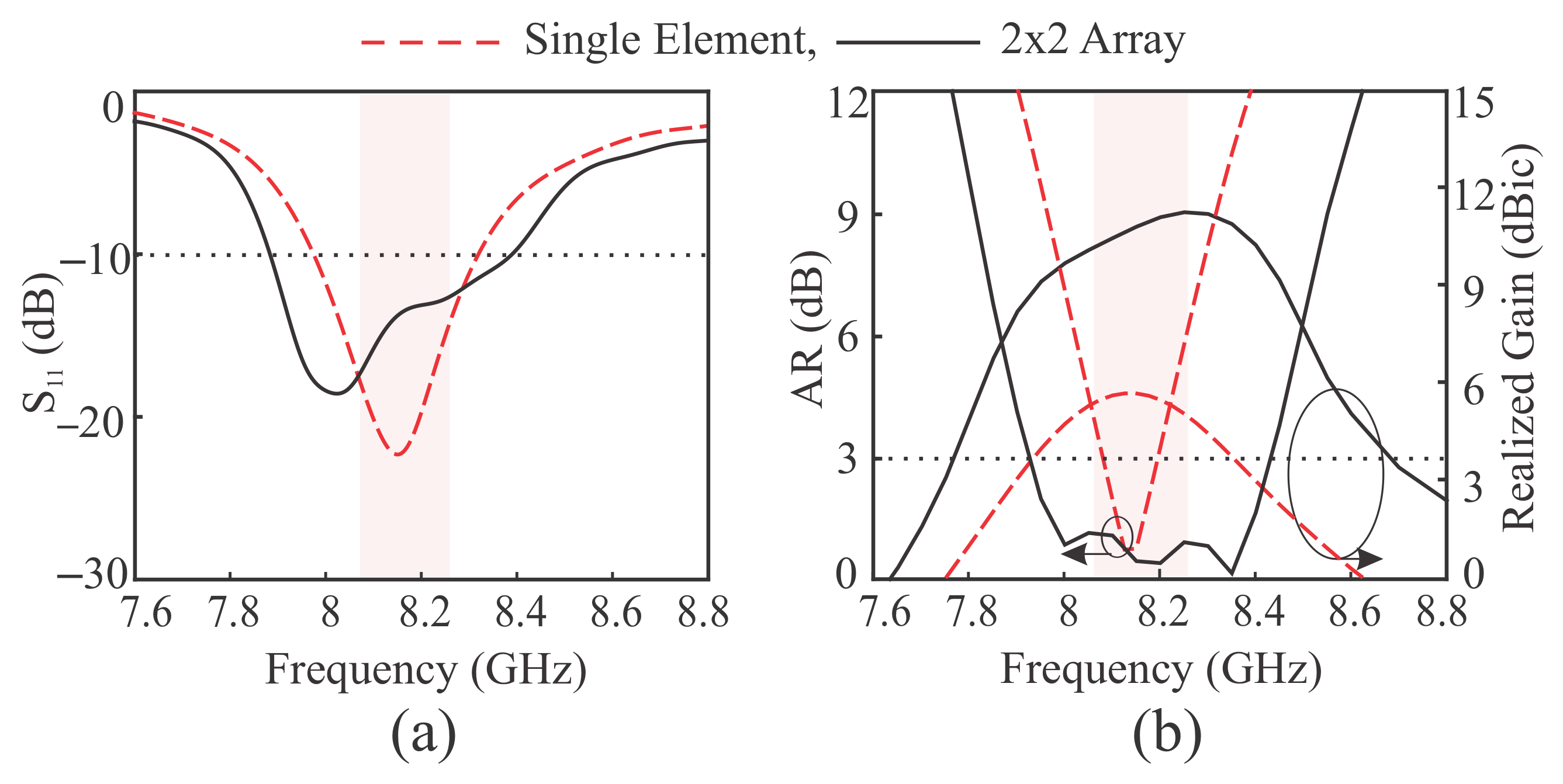
3.2. Application of SP Feed in 2 × 2 Antenna Array

To illustrate the presented SP feed with applications to 2 × 2 arrays, we employed a CP patch for an antenna element with a 0.35 λ g × 0.35 λ g SP feed. The array performance is optimized with the compact size that has the distance between the centers of the elements, 19.73 mm (0.535 λ 0 ). Figure 4b shows the geometry of the optimized design of the 2 × 2 arrays with the SR phase feeding structure. Figure 5 shows the improved performance of the 2 × 2 array, compared to the single patch antenna. The IBW of the single patch is from 7.95–8.32 GHz that covers the uplink band for satellite application. The maximum realized gain of the antenna is 5.4 dBi and the overlapping ARBW is from 8.12–8.22 GHz. In the case of array, the AR and gain level performances both appeared to undergo improvements. The IBW of the 2 × 2 array is 7.88–8.42 GHz and the ARBW of 7.92–8.42 GHz with the peak LHCP gain of 11.5 dBic. In this illustration, the impedance is designed at 50 Ω for the antenna elements and the input ports. The plots of co-pol radiation patterns at five frequency samples in the bandwidth are given in Figure 6. It can be seen that there is asymmetry in the radiation patterns with respect to the broadside direction in two planes, which is caused by the non-uniformity in the structure of the array due to the feed line. The asymmetry gets decreases at high frequencies in the band. However, the peak gain of the main lobe is along the broadside directions. The side lobe levels lie near −10 dBic. Table 2 summarizes the comparison of our work with earlier studies in terms of 3 dB ARBW, CP gain, and compactness (C-to-C distance). The gain in [17,18,20] is lower as compared to the proposed compact design. Unlikely, the size of the [21] is comparatively smaller as compared to the proposed work, but it results in a very low gain. The gain of 13.5 dBic in [19] is higher because of the larger distance between the centers of the elements. Similarly, the gain of 14.25 dBic is achieved in [22] by using the air gap in multiple layers. Thus, the design is bulky as well as a larger C-to-C distance among the elements. The ARBW of the design in [18] is 7.6%, which is just greater by 0.66% than the ARBW of the proposed design. Unlikely, the ARBW in [19] is very low that is 1.3%. In all of the above literature, the designs have higher gain at the expense of the size. Finally, the design in [23] is very compact that has a higher 3 dB ARBW but the gain is low as compared to the proposed work. Despite the compact structure, the gain is improved by using parasitic patches to increase the radiation surface. The main issue of this compact structure is that the main beam at different frequencies has deviated from the broadside direction. Second, this design cannot be extended to 4 × 4 array with this configuration on a single layer to achieve high gain. For this purpose, the feed should be on the second layer, which increases the fabrication cost. On the other hand, the proposed structure can easily be extended to 4 × 4 array on a single layer. Furthermore, the main beam of the proposed design is along the broadside direction. The aim of our work is to maintain a certain level of gain in ±10 range with respect to the broadside direction. Otherwise, the tilt in the main beam degrades the gain in desired direction.
In practical applications, like small satellites for next-generation, just a 3 dB ARBW criteria is not acceptable. The AR must be lower than 1.5 dB with an acceptable level of gain up to 12 dBic in the angular width of ±10 . Therefore, in the next section, a 4 × 4 CP antenna array that is based on the compact 2 × 2 array fed by a multistage SR feeding network is designed and experimentally verified, which satisfies the requirements of the next-generation small satellite application.

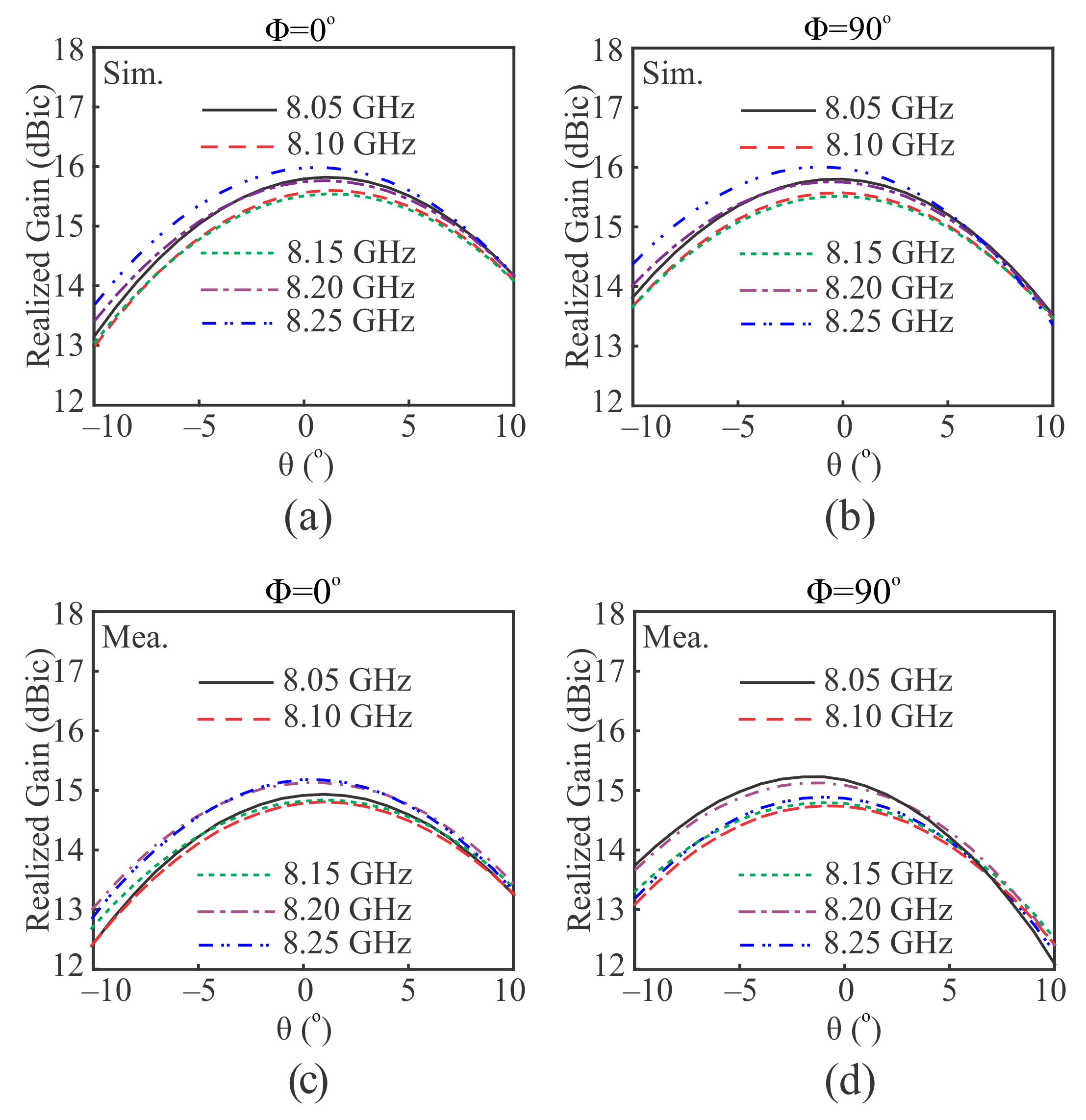
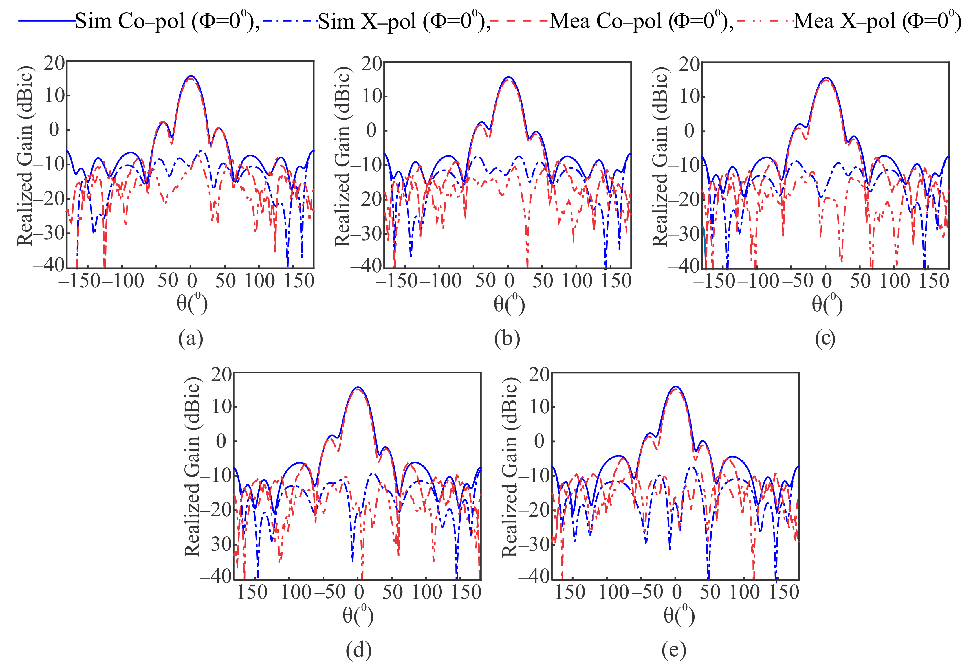
3.3. 4 × 4 Antenna Array and Measurements

As mentioned earlier, the purpose is to achieve a gain of 12 dBic with minimal AR less than 1.5 dB in the angular width of ±10 . Thus, the SP feed can easily be extended to the large CP array for high-gain applications. Using the compact and uniform features, the presented 2 × 2 SP feed and array elements can be repeated and iteratively extended to the larger scale array. Figure 7 shows the configuration and prototype of 4 × 4 array using the group-and-repeat process based on the module unit of the presented 2 × 2 feed of 0.35 λ g × 0.35 λ g along with the prototype. The overall size of the array is 3.48 λ g × 3.48 λ g . The simulated and measured results for the reflection coefficients, realized gain, and AR of the design are compared in Figure 8. Improvements in the IBW, AR, and LHCP gain have been observed. The S 11 of the proposed antenna array is measured using the Agilent 85052D network analyzer. The measured IBW for S 11 ≦−10 dB is essentially greater than 19.5%, as shown in Figure 8a. The behavior of the simulation and measured reflection coefficients are similar but differ by large values, which can be attributed to the fabrication tolerance. The simulated and measured AR and gain of the array are shown in Figure 8b. The measured ARBW of the array is based on the requirement of the application (AR ≦ 1.5 dB) is 7.23% (7.86 GHz to 8.45 GHz). However, the measured 3 dB ARBW of the array is 8.8% (7.8 GHz to 8.52 GHz). The gain varied between 12.5 dBic and 15.5 dBic in the 3 dB ARBW. A standard dual-polarized horn antenna was used to measure the total gain characteristics of the proposed design. Figure 9 shows the simulated and measured LHCP gain in the angular width of ±10 in ϕ = 0 and ϕ = 90 planes. Five frequency samples were chosen to depict the performance across the bandwidth. The overall difference in the measured and simulated LHCP gain is 0.5 dB. It can be observed that the measured LHCP gains at all frequencies are higher than 12.5 dBic in the ϕ = 0 plane, as shown in Figure 9c, whereas in ϕ = 90 plane, the measured LHCP gains are higher than 12 dBic as seen in Figure 9d. Similarly, the simulated and measured ARs of the array are plotted in Figure 10. The measured AR performance in ϕ = 0 plane shows that the AR lies below 1.5 dB for all frequencies in ±10 span, but at 8.05 GHz it is slightly above 1.5 dB at +10 . In ϕ = 90 plane, AR values for all frequencies are lower than 1.5 dB in the desired angular width except 8.05 GHz that crosses 1.5 dB level by 0.15 dB at +10 and −10 of the angular space. The co- and cross-pol (X-pol) radiation patterns of the array antenna are measured and compared with simulated results in Figure 11 and Figure 12 in two planes, ϕ = 0 and ϕ = 90 , respectively, at five frequency samples. The measured co-pol patterns agree well with simulated results. The difference in the gain of the main lobes and sidelobes varies from 13.4 dB to 14.5 dB in the ϕ = 0 plane, whereas this difference is larger in ϕ = 90 plane that is from 13.8 dB to 15.8 dB. The measured X-pol levels are below −15 dBic in the broadside direction. Table 3 compares the presented work with the previous literature. The designs in [24,25] are very compact with the C-to-C distance of 0.48 λ 0 and 0.45 λ 0 between the elements. Both the designs achieve low measured peak gains of 12.5 dBic. In [24], the IBW and 3 dB ARBW of the array are very narrow but in [25] these are wider as compared to the proposed design. Similarly, the design in [26] bears wide IBW and ARBW of 14.7% and 12.4%, respectively. The E-to-E distance among the elements is 0.74 λ 0 which bears a high gain of 18 dBic. A design with a similar E-to-E distance has been given in [27], which results in a narrow IBW of 6.08% and ARBW of 4.4%. Moreover, the manuscript lacks information about the maximum gain. The proposed design is compact that has the C-to-C distance of 0.535 λ 0 with a gain of 15.5 dBic. The proposed design achieves good performance in terms of gain as [24,25]. Similarly, the performance of the design in [26] is better at the cost of larger size. Finally, the proposed design has higher IBW and ARBW as compared to [27] despite the small size. Furthermore, the proposed design has been analyzed in terms of LHCP gain and AR within a certain degree of angular width, which is the requirement of the satellite application. The LHCP gain is maintained above 12 dBic and AR below 1.5 dB in the angular width that ranges from −10 to +10 in the whole bandwidth. Regarding the radiation pattern, these are stable in both the planes.

4. Conclusions

In this paper, a compact wideband CP microstrip antenna array for the next generation small satellite application in the Ku-band was designed, simulated, and fabricated. The array is based on the iterative application of the SR phase feeding network. The elements have the C-to-C distance of 0.535 λ 0 at the designed frequency of 8.15 GHz. The IBW of the design is greater than 19.5% and AR is 8.8% (7.8 to 8.52 GHz), respectively. A measured peak gain of 15.5 dBic is achieved at 8.25 GHz. The design has a flat gain that varied from 15 dBic to 15.5 dBic in the desired bandwidth from 8.05 GHz to 8.25 GHz. Moreover, the design performance is measured for the gain and AR in the angular width from −10 to +10 in the Ku-band that validated the gain is greater than 12 dBic and AR is less than 1.5 dBic. The co- and X-pol radiation patterns at five frequency samples are measured in the band that agrees with the simulation results.

Author Contributions

M.E., S.T.-V., Y.Y., K.-Y.L. and K.-C.H. contributed to conceptualization, articulation, original draft preparation, review and the editing of the document. All authors have read and agreed to the published version of the manuscript.

Funding

This work was supported by Institute of Information & communications Technology Planning & Evaluation (IITP) grant funded by the Korea government(MSIT) (No.2020-0-00261, Development of low power/low delay/self-power suppliable RF simultaneous information and power transfer system and stretchable electronic epineurium for wireless nerve bypass implementation.

Institutional Review Board Statement

Not applicable.

Informed Consent Statement

Not applicable.

Data Availability Statement

Not applicable.

Conflicts of Interest

The authors declare no conflict of interest. The funders had no role in the design of the study; in the collection, analyses or interpretation of data; in the writing of the manuscript or in the decision to publish the results.

References

  1. Gao, S.S.; Luo, Q.; Zhu, F. Circularly Polarized Antennas; John Wiley & Sons: Hoboken, NJ, USA, 2013. [Google Scholar]
  2. Ta, S.X.; Park, I. Planar wideband circularly polarized metasurface-based antenna array. J. Electromagn. Waves Appl. 2016, 30, 1620–1630. [Google Scholar] [CrossRef]
  3. Nosrati, M.; Yang, C.; Liu, X.; Tavassolian, N. Wideband circularly polarized, slot antenna array loaded with metasurface. Microw. Opt. Technol. Lett. 2020, 62, 2976–2988. [Google Scholar] [CrossRef]
  4. Le, T.T.; Tran, H.H.; Althuwayb, A.A. Wideband Circularly Polarized Antenna Based on a Non-Uniform Metasurface. Appl. Sci. 2020, 10, 8652. [Google Scholar] [CrossRef]
  5. Nkimbeng, C.H.S.; Wang, H.; Park, I. Coplanar Waveguide-Fed Bidirectional Same-Sense Circularly Polarized Metasurface-Based Antenna. J. Electromagn. Eng. Sci. 2021, 21, 210–217. [Google Scholar] [CrossRef]
  6. Wang, R.; Jiao, Y.; Lu, L.; Zhang, H. A novel wideband circularly polarized patch array with meta-surface. Appl. Sci. 2016, 62, 1–8. [Google Scholar] [CrossRef] [Green Version]
  7. Zheng, Q.; Guo, C.; Vandenbosch, G.A.; Ding, J. Low-profile circularly polarized array with gain enhancement and RCS reduction using polarization conversion EBG structures. IEEE Trans. Antennas Propag. 2019, 68, 2440–2445. [Google Scholar] [CrossRef]
  8. Rajanna, P.K.T.; Rudramuni, K.; Kandasamy, K. A wideband circularly polarized slot antenna backed by a frequency selective surface. J. Electromagn. Waves Appl. 2019, 19, 166–171. [Google Scholar] [CrossRef]
  9. Li, H.; Du, X.; Wei, Z.; Zhou, Z.; Yin, Y.Z. Broadband low-profile circularly polarized antenna with stepped sequential feeding structure. Prog. Electromagn. Res. 2018, 78, 1–7. [Google Scholar] [CrossRef] [Green Version]
  10. Wang, L.; En, Y.F. A Wideband Circularly Polarized Microstrip Antenna With Multiple Modes. IEEE Open J. Antennas Propag. 2020, 1, 413–418. [Google Scholar] [CrossRef]
  11. Tran, H.H.; Ta, S.X.; Park, I. Single-feed, wideband, circularly polarized, crossed bowtie dipole antenna for global navigation satellite systems. J. Electromagn. Eng. Sci. 2014, 14, 299–305. [Google Scholar] [CrossRef]
  12. Ta, S.X.; Han, J.J.; Park, I.; Ziolkowski, R.W. Wide-beam circularly polarized crossed scythe-shaped dipoles for global navigation satellite systems. J. Electromagn. Eng. Sci. 2013, 13, 224–232. [Google Scholar] [CrossRef] [Green Version]
  13. Ta, S.X.; Han, J.J.; Park, I. Compact circularly polarized composite cavity-backed crossed dipole for GPS applications. J. Electromagn. Eng. Sci. 2013, 13, 44–50. [Google Scholar] [CrossRef]
  14. Hall, P.S.; Hall, C.M. Coplanar corporate feed effects in microstrip patch array design. IEE Proc. H (Microw. Antennas Propag.) 1988, 135, 180–186. [Google Scholar] [CrossRef]
  15. Hall, P.S.; Dahele, J.S.; James, J.R. Design principles of sequentially fed, wide bandwidth, circularly polarised microstrip antennas. IEE Proc. H (Microw. Antennas Propag.) 1989, 136, 381–389. [Google Scholar] [CrossRef]
  16. Evans, H.; Gale, P.; Aljibouri, B.; Lim, E.G.; Korolkeiwicz, E.; Sambell, A. Application of simulated annealing to design of serial feed sequentially rotated 2 × 2 antenna array. Electron. Lett. 2000, 36, 1987–1988. [Google Scholar] [CrossRef]
  17. Maddio, S. A Compact Wideband Circularly Polarized Antenna Array for C-band Applications. IEEE Antennas Wirel. Propag. Lett. 2015, 14, 1081–1084. [Google Scholar] [CrossRef]
  18. Zhao, H.; Shui, M.; Deng, W.; Fang, Z.; Jiang, Z. Broadband Circularly polarized Sequential-Rotation Array Antenna with Compact Sequential-Phase Feed. Cross Strait-Quad-Reg. Radio Sci. Wirel. Technol. (CSQRWC) 2018, 14, 1–3. [Google Scholar]
  19. Chen, A.; Zhang, Y.; Chen, Z.; Cao, S. A ka-band highgain circularly polarized microstrip antenna array. IEEE Antennas Wirel. Propag. Lett. 2010, 9, 1115–1118. [Google Scholar] [CrossRef]
  20. Xu, P.; Yan, Z.-H.; Zhang, T.-L.; Yang, X.-Q. Broadband circularly polarized slot antenna array using a compact sequential-phase feeding network. Prog. Electromagn. Res. 2014, 47, 173–179. [Google Scholar] [CrossRef] [Green Version]
  21. Piroutiniya, A.; Rasekhmanesh, M.H.; Mohammadi, P. Wide-band circularly polarised antenna array using sequential phase feed structure and reinforced square radiating patch element. IET Microwaves Antennas Propag. 2018, 12, 1395–1399. [Google Scholar] [CrossRef]
  22. Evans, H.; Sambell, A. Wideband 2 × 2 sequentially rotated patch antenna array with a series feed. Microw. Opt. Technol. Lett. 2004, 40, 292–294. [Google Scholar] [CrossRef]
  23. Zou, Y.; Li, H.; Xue, Y.; Sun, B. A high-gain compact circularly polarized microstrip array antenna with simplified feed network. Int. J. RF Microw. Comput.-Aided Eng. 2019, 29, e21964. [Google Scholar] [CrossRef]
  24. Daniele, I.; Hu, W.; Wen, G. Design of a microstrip series power divider for sequentially rotated nonuniform antenna array. Int. J. Antennas Propag. 2017, 2017, 9482979. [Google Scholar]
  25. Maddio, S. A compact two-level sequentially rotated circularly polarized antenna array for C-band applications. Int. J. Antennas Propag. 2015, 2015, 830920. [Google Scholar] [CrossRef] [Green Version]
  26. Evans, H.; Gale, P.; Sambell, A. Performance of 4 × 4 sequentially rotated patch antenna array using series feed. Electron. Lett. 2003, 39, 493–494. [Google Scholar] [CrossRef]
  27. Jazi, M.N.; Azarmanesh, M.N. Design and implementation of circularly polarised microstrip antenna array using a new serial feed sequentially rotated technique. IEE Proc.-Microw. Antennas Propag. 2006, 153, 133–140. [Google Scholar] [CrossRef]
Figure 1. Configuration of sequential-phase (SP) feed and 2 × 2 SR CP array.
Applsci 11 08869 g001
Figure 2. SR phase feed network (a) Topology (b) Equivalent circuit model: (w f = 1.7, w 1 = 0.186, w 2 = 0.595, w 3 = 0.159, w 4 = 0.367, w 5 = 0.495, w 6 = 0.1, w 7 = 0.595, w p = 1.8, w s = 1, l 0 = 3.8, l 1 = 3.25, l 2 = 5.58, l 3 = 4.24, l 4 = 4.82, l 5 = 4.52, l 6 = 4.25, l 7 = 5.27, l s = 0.888) mm , (Z f = 50, Z 0 = 50, Z 1 = 113.03, Z 2 = 80.01, Z 3 = 117.25, Z 4 = 94.01, Z 5 = 85.39, Z 6 = 129.23, Z 7 = 80.01, Z 7 = 64.65 ) Ω .
Applsci 11 08869 g002
Figure 3. Performance of SR phase feed: (a) S-parameters of SR feed with open stub. (b) Phase difference of the signals between the consecutive output ports with open stub. (c) S-parameters of SR feed without open stub. (d) Phase difference of the signals between the consecutive output ports without open stub.
Applsci 11 08869 g003
Figure 4. Configuration of (a) Single element. (b) 2 × 2 SR arrays using the presented SP feed: (w f = 1.7, l 1 = 4.495, l s t u b = 1.6, l 2 = 0.945, w c = 1.485, w p = 6.74, w 1 = 0.186 mm).
Applsci 11 08869 g004
Figure 5. Comparison of the performance between single element and 2 × 2 array: (a) Reflection coefficient. (b) AR and LHCP gain.
Applsci 11 08869 g005
Figure 6. Simulated co-pol radiation patterns of 2 × 2 array at five frequency samples in ϕ = 0 and ϕ = 90 plane: (a) 8.05 GHz (b) 8.10 GHz. (c) 8.15 GHz. (d) 8.20 GHz. (e) 8.25 GHz.
Applsci 11 08869 g006
Figure 7. A 4 × 4 CP array antenna: (a) Optimized design. (b) Photo of prototype.
Applsci 11 08869 g007
Figure 8. Comparison of simulated and measured results: (a) Reflection coefficients. (b) AR and LHCP gain.
Applsci 11 08869 g008
Figure 9. LHCP gains at five frequency samples in the angular range of ±10 : (a) Simulated LHCP gain in the ϕ = 0 . (b) Simulated LHCP gain in ϕ = 90 . (c) Measured LHCP gain in the ϕ = 0 . (d) Measured LHCP gain in ϕ = 90 .
Applsci 11 08869 g009
Figure 10. AR at five frequency samples in the angular range of ±10 : (a) Simulated AR in the ϕ = 0 . (b) Simulated AR in ϕ = 90 . (c) Measured AR in the ϕ = 0 . (d) Measured AR in ϕ = 90 .
Applsci 11 08869 g010
Figure 11. Simulated and measured radiation patterns of 4 × 4 array at five frequency samples in ϕ = 0 plane: (a) 8.05 GHz (b) 8.10 GHz. (c) 8.15 GHz. (d) 8.20 GHz. (e) 8.25 GHz.
Applsci 11 08869 g011
Figure 12. Simulated and measured radiation patterns of 4 × 4 array at five frequency samples in ϕ = 90 plane: (a) 8.05 GHz (b) 8.10 GHz. (c) 8.15 GHz. (d) 8.20 GHz. (e) 8.25 GHz.
Applsci 11 08869 g012
Table 1. Specifications of the 4 × 4 array antenna of the satellite application.
TypeIBW/ARBW
(GHz)
PolarizationGain (dBic)Angular
Width
AR (dB)
4 × 4 Array8.05–8.25LHCP>12±10 in two
planes
<1.5
Table 2. Comparison of the proposed single-feed 2 × 2 CP array antenna with the earlier ones.
Ref.TypeARBW(%)CP
Gain(dBic)
C-to-C
( λ 0 )
Distance
[17]Single Layer15.58.250.5
[18]Single Layer7.610.040.99
[19]Single Layer1.313.50.87
[20]Single Layer588.90.72
[21]Single Layer507.80.46
[22]Multi-Layer with air gap17.514.250.74
[23]Single Layer11.29.80.4
[Prop.]Single Layer6.93511.50.535
Table 3. Comparison of the proposed single-feed 4 × 4 CP array antenna with the earlier ones.
Ref.TypeFeeding
Mechanism
IBW
(%)
3 dB AR (%)CP Gain
(dBic)
C-C/E-E
( λ 0 )
Distance
[24]Single LayerSR feed2.72.712.50.48 (C-C)
[25]Single LayerSR feed5316.5 and 10.3712.50.45 (C-C)
[26]Single LayerSR feed14.712.4180.74 (E-E)
[27]Single LayerSR feed6.084.4NG0.74 (E-E)
This workSingle LayerSR feed>19.58.815.50.535 (C-C)
Publisher’s Note: MDPI stays neutral with regard to jurisdictional claims in published maps and institutional affiliations.

