Article

Design of a Rectangular Pickup Coil Fabricated on a PCB Using WBG Power Semiconductor in Discrete Package

Department of Electrical and Biomedical Engineering, Hanyang University, Seoul 04763, Korea
Appl. Sci. 2021, 11(5), 2290; https://doi.org/10.3390/app11052290
Submission received: 5 February 2021 / Revised: 27 February 2021 / Accepted: 1 March 2021 / Published: 4 March 2021
(This article belongs to the Section Electrical, Electronics and Communications Engineering)

Abstract

:
Power semiconductors based on wide bandgap (WBG) devices are capable of fast switching and have low on-resistance. Accordingly, a fast sensor with a higher bandwidth is required for circuit inspection based on switch current measurements. Thus, it is necessary to have a current sensor in the printed circuit board (PCB) circuit for diagnosis and protection of the surface mount device (SMD) type circuit system. Accordingly, a pickup coil with the advantages of a high degree of sensor configuration freedom, wide bandwidth, and low cost can be a good alternative. This study analyzes the influence of coil shape and parameters on sensor design as a guideline for embedding a pickup coil in an SMD-type PCB circuit of a WBG power semiconductor-based, half-bridge structure. The mutual inductance and self-inductance values of the coil are considered large variables in the design of a sensor coil for simultaneously maintaining high bandwidth and sensor sensitivity. Therefore, magnetic and frequency response analyses were conducted to verify the correlation with inductance, the influence of coupling capacitance, and the influence of the magnetic field formation via the current flowing through the external trace inside the PCB. The coil model is verified and discussed through simulation and double pulse tests.

1. Introduction

A system that includes a power semiconductor based on a wide bandgap (WBG) device has the advantages of high di/dt, dv/dt, efficiency, and a fast-switching speed, compared to conventional silicon devices [1,2]. Therefore, WBG devices are attracting much attention in the industry and related research pursuing small size and low-cost devices; in particular, GaN devices have remarkably fast switching characteristics among WBG devices; hence, the issues of stability and system protection in transient response situations are major issues that need to be resolved in the development and use of GaN devices [3,4,5,6]. At this time, the stability of a system is based on accurate and fast measurement information during the switch operation. Therefore, it is necessary to follow the step change of the current well. Otherwise, when measuring current, excessive peak current may cause malfunction of the already established protection operation.
To measure the switch current of the power semiconductor embedded in the PCB [7,8], current sensor technologies based on sensor evaluation criteria such as a minimum area with sufficient bandwidth, insulation, and sufficient sensitivity are required. The toroidal Rogowski coil is a representative insulation sensor and can be a viable current sensor candidate for WBG devices based on its relatively wide bandwidth, small size, and linear characteristics. Basically, in toroidal Rogowski coils, which are a type that wraps the conductor of the primary current in all directions [9,10,11], the position between the coil and the conductor has a great influence on the measurement accuracy [12,13], and the study conducted in [14] minimizes the position error between the sensor and conductor. In the paper of [15,16,17], a PCB-based Rogowski coil model that can minimize the position error between the sensor and the conductor was proposed; [18,19,20] described the application of this PCB-based toroidal Rogowski coil for system protection. However, the PCB-based Rogowski coil discussed in this paper was only applied to the power semiconductor of module type, and [20] demonstrated higher performance than DeSat protection.
The shape of the Rogowski coil and the different design structures in the PCB circuit can have a significant influence on the bandwidth, sensitivity, and external noise that appear through different magnetic properties. Accordingly, studies on various coil shapes and designs have been studied to increase bandwidth and improve sensitivity and noise immunity, and their influence has been analyzed [21,22]. In [23,24,25], a differential Rogowski coil with insulation characteristics was proposed to reduce the coupling capacitance noise of the conventional Rogowski coil. In [26], a current sensor with a rolling trace was proposed to maximize the bandwidth of the Rogowski coil in the PCB. In [27,28], a spiral-type Rogowski coil structure was proposed to improve the sensitivity of the coil. Moreover, a guideline for the optimal coil shape was presented through the analysis of the mutual inductance, according to the coil type [29]. However, it is impossible to embed a conventional toroidal-type Rogowski coil in a PCB, including a non-modular power converter; hence, a pickup coil was proposed in [30,31,32,33,34]. The pickup coil uses the same sensor method as the existing Rogowski coil in a large category and, according to Maxwell–Faraday law, an electromotive force (EMF) is induced at the output end of the coil loop through the coil structure in which a part of the magnetic flux generated by the primary current flows into the closed-loop area of the coil. The current sensor configuration of the rolling structure shown in [26] can secure a higher bandwidth than a conventional sensor configuration, and hence a pickup coil with such a rolling structure is proposed in [30]. In particular, pickup coils, which have higher degrees of design freedom than conventional toroidal Rogowski coils, can be affected by various magnetic fluxes according to the corresponding design configuration and can have various mutual inductance and self-inductance values. However, due to the characteristics of the pickup coil, which is composed of a built-in PCB, external conductors significantly influence the PCB [33].
This study analyzes the influence of external wires on the sensor in the PCB and the influence of coil parameters for a pickup coil configuration that measures the switch current in a half-bridge structure system, employing a non-modular WBG power semiconductor. The process of analyzing the mutual inductance is performed by comparing the magnetic flux and bandwidth between the five pickup coil models according to the configurable coil and conductor shape.
The remainder of this paper is organized as follows. Section 2 covers the basics of PCB-embedded pickup coils, and Section 3 deals with the influence of each coil parameter through the magnetic flux and mathematical analysis. Section 4 addresses the experimental verification of this study, and Section 5 provides the conclusion.

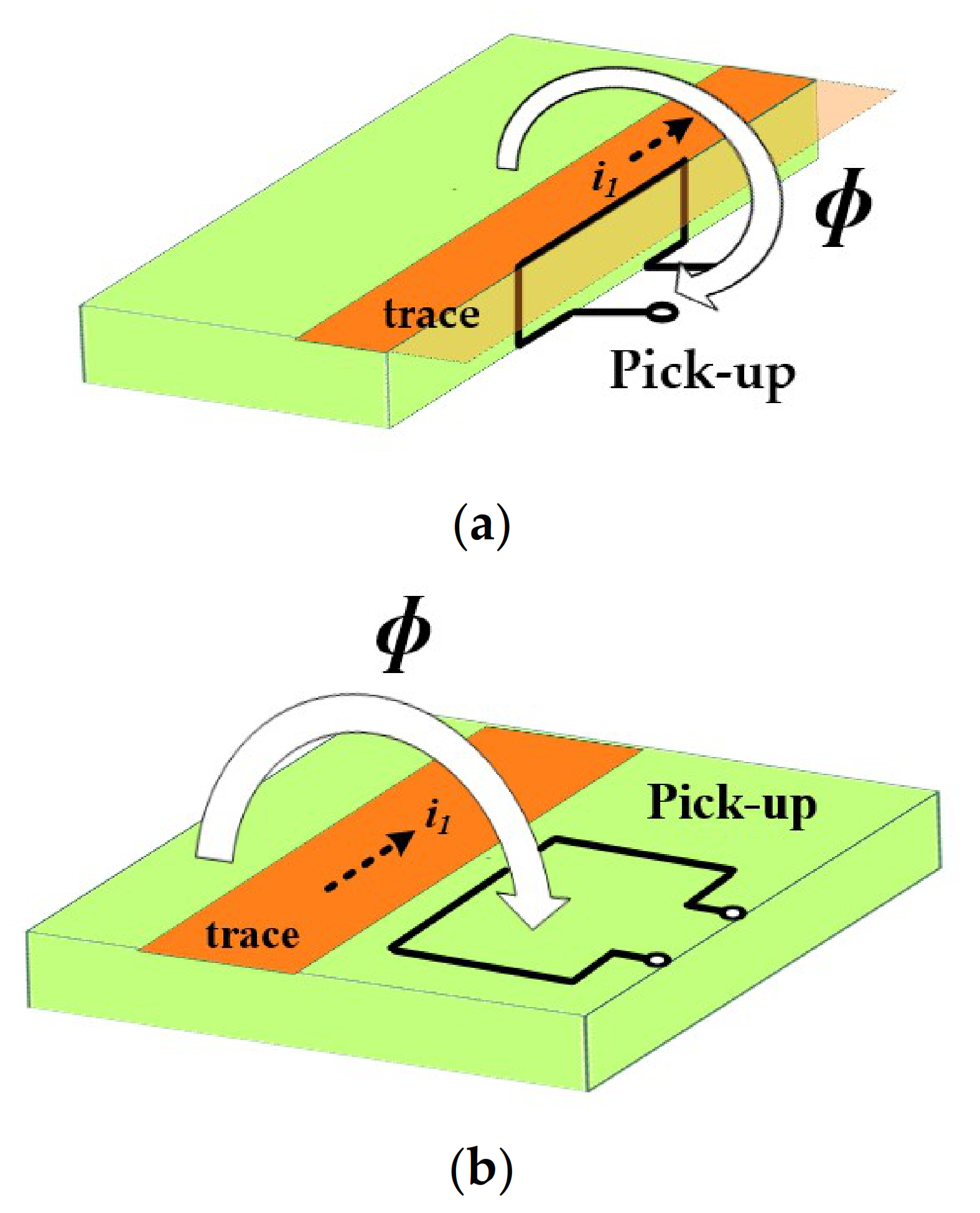
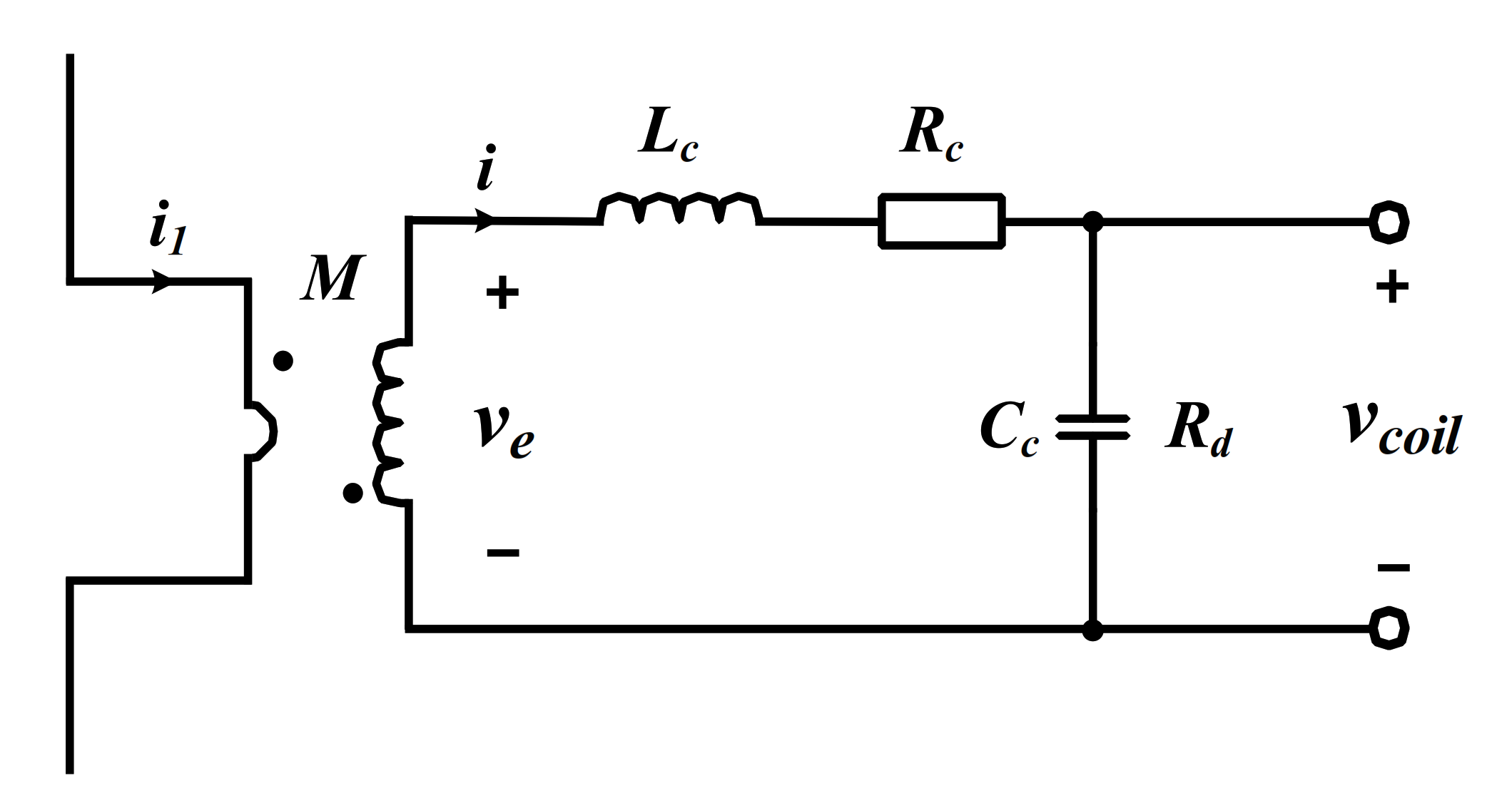
2. Basics of a Pickup Coil

While measuring the switch current of power semiconductors in discrete packages or measuring the current flowing through the PCB trace, there are many difficulties in configuring the existing toroidal Rogowski coil; these difficulties can be addressed via a pickup coil configuration. Figure 1 shows the pickup coil structure in two cases that can be embedded in the PCB. Figure 1a shows the case of a coil configured at a vertical position, concerning the trace through which the primary current i1 flows and the coil thickness corresponds to the height at which the magnetic flux is received; it is possible to configure a coil with a large number of turns. In the case of Figure 1a, it corresponds to the model of the existing pickup coil [30,33]. Figure 1b shows a coil configured in a horizontal position to trace the primary current i1 flows. This coil is configured in a horizontal position to receive the magnetic flux of the primary current on the same PCB layer [34]. The number of turns is limited according to the number of layers because it increases or decreases in size according to the number of layers. For both coil models, the magnetic flux formed by the primary current i1 passes through the inside of the closed-loop area in the coil, and an EMF is induced at the output end of the loop following Maxwell–Faraday law.
Therefore, it is necessary to consider the influence of the position of the external conductor in situations in which accurate switch current measurement in case ofdesigning the pickup coil in PCB is required.
Figure 2 is an equivalent circuit analyzed with a lumped model for a pickup coil and Lc is the magnetization inductance of the coil, Rc is the self-resistance value of the coil, Cc is the self-capacitance value of the coil, and M denotes the mutual inductance between the coil and conductor.
G c o i l ( s ) = v c o i l ( s ) i 1 ( s ) = M s ( L c C c ) s 2 + s ( L c + R c R d C c R d ) + R c + R d R d
When the primary current i1 flows through the trace, the density B of the flux density around conductor trace by the Biot–Savart law is basically formed by the magnetic field intensity H as follows:
B = μ H = μ i 1 2 π r
where r is away from the conductor to the measurement point, and μ is relative magnetic permeability. The generated flux passes through the S area, the amount of generated magnetic flux ϕ in that area is as follows:
ϕ = S B d s
where µo is the relative magnetic permeability, ds is the smallest section of area S, and the EMF induced at the output stage of the coil is,
v e t = d ϕ d t = M d i 1 d t
where M represents the mutual inductance between the coil and the conductor, itdetermines the sensitivity of the sensor. If M is increased by increasing the self-inductance, the sensitivity of the sensor also increases; however, at the same time, the bandwidth of the coil is reduced due to the high Lc. This can reduce accuracy when measuring the switch current for fast power semiconductor devices such as GaN. At this time, the bandwidth of the sensor is as follows [31]:
fc ≤ Bandwidth ≤ fcoil_pole
f c o i l _ p o l e = 1 2 π R c + R d L c R d C c 1 2 π L c C c
where fcoil_pole is the pole frequency of Gcoil in Equation (1).
To configure a current sensor using a coil in a specific bandwidth with high sensitivity for a fast device such as GaN, a coil design capable of significantly lowering the Lc/M value is required. Therefore, the analysis of the coil in this paper proceeds based on the performance parameter Lc/M.

3. Analysis of Parameter for Designing Pickup Coil in PCB

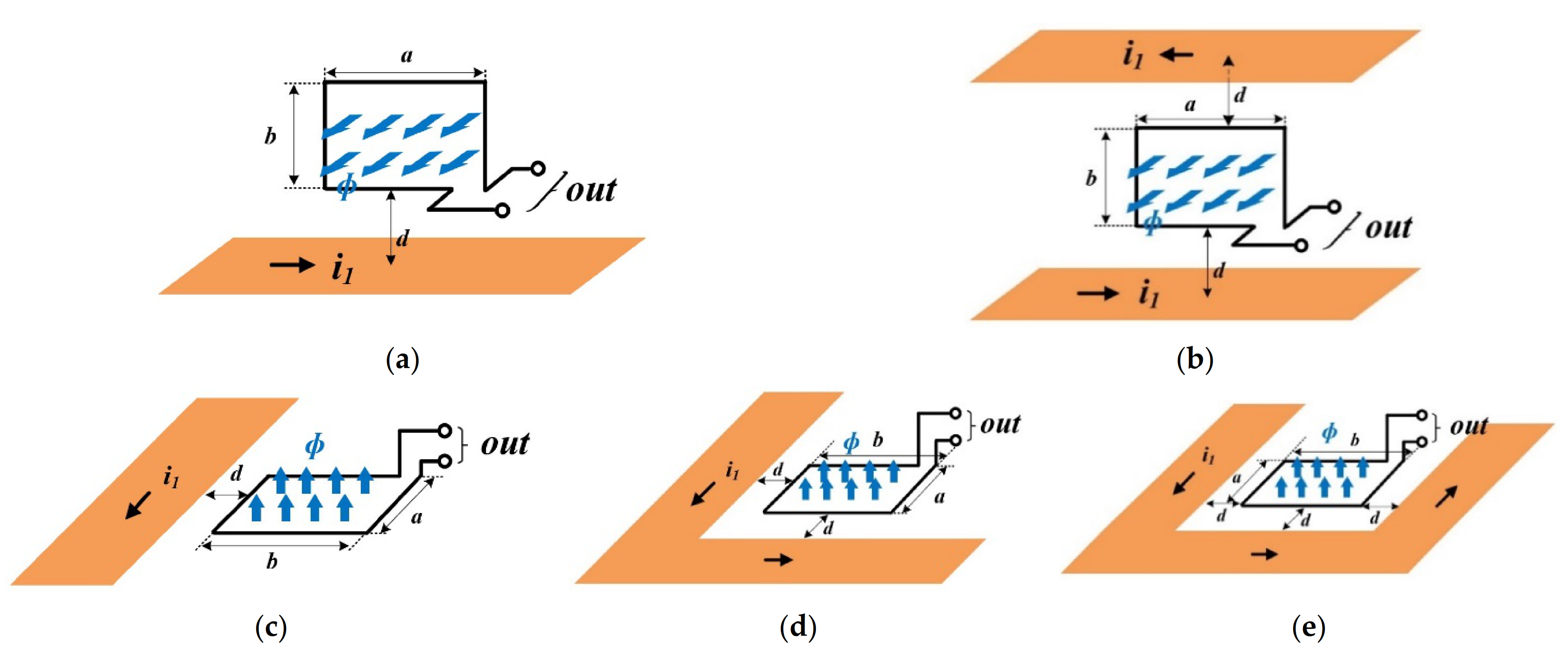
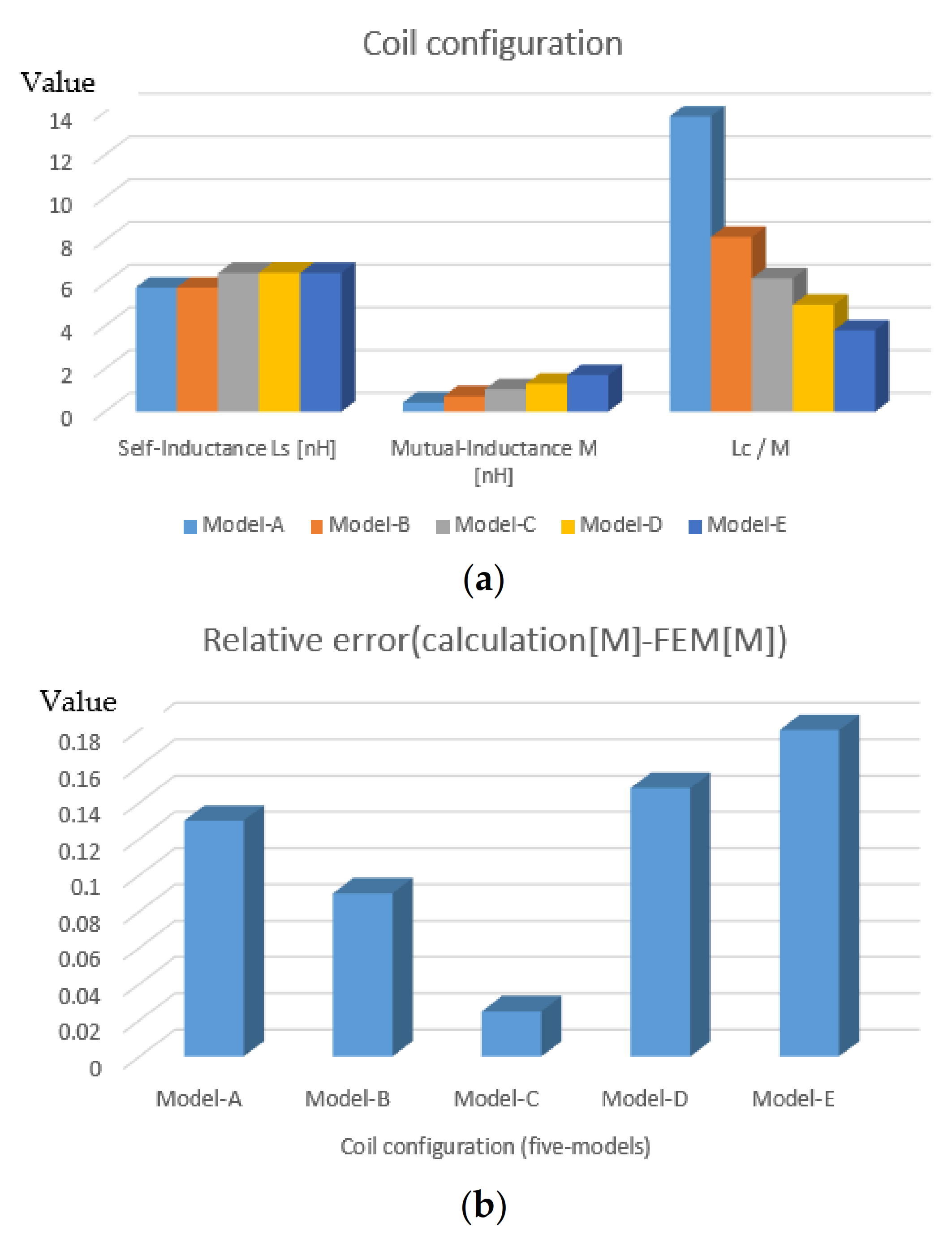
3.1. Pickup Coil Configuration in PCB

PCB-embedded pickup coils have various mutual inductance values according to their position and shape. The distance between the coil and conductor through which the primary current flows, the shape, and the turn number of the coil determines the amount of magnetic flux incident on the closed-loop area of the coil formed by the primary current, and thus affects the EMF value. Each of the five models in Figure 3 depicts five structures in which a single-turn rectangular pickup coil can be placed on the PCB. These five models are classified according to the number of traces through which the primary current flows adjacent to the pickup coil. In all coil models, the self-inductance value can be flexibly determined by varying the number of turns and coil size.
The pickup coil depicted in Figure 3a is the most basic coil model, and it consists of the trace primary current flowing on the bottom layer of the PCB and a coil composed of pattern and vias, where the magnetic flux incident surface is located in the vertical direction to the trace, i.e., the magnetic flux formed by one side of the conductor trace through which the primary current is flowing enters the magnetic flux incident area of the pickup coil [30,34].
In this case, the distance d is determined as a small value equal to the PCB layer thickness level. According to Maxwell–Faraday law, the amount of total magnetic flux ϕA through the flux incident area S is the integral value of the magnetic flux density B, as shown below. All mathematical analysis methods assumed the shape of the virtual wire, not the shape of the trace.
ϕ A = S B d s = μ o i 1 2 π d b + d 1 b a d b = μ o a i 1 2 π ln b + d d
where μo is the air permeability. The EMF voltage vA is induced at the coil output terminal, as follows:
v A ( t ) = M 1 d i 1 d t = d ϕ d t = μ o a 2 π ln b + d d d i 1 d t
In addition, the mutual inductance MA between the conductor and the coil is as follows:
M A = μ o a 2 π ln b + d d
Figure 3b shows the coil structure in which the magnetic flux incident surface of the pickup coil is positioned perpendicular to the trace in the situation of the primary current flowing through the via and two traces in the upper and lower layers. The magnetic flux generated by the primary current flowing at the top and bottom is incident inside the coil in the same direction [30]. The amount of magnetic flux incident ϕB, in this case, is doubled compared to the previous case.
ϕ B = μ o a i 1 π ln b + d d
The mutual inductance MB between the conductor and coil is as follows:
M B = μ o a π ln b + d d
Unlike Model-A and B, in Model-C, D, and E, the coil is positioned horizontallyconcerning the trace through which the primary current flows. Therefore, to construct a multi-turn coil, the number of coil turns must be increased or decreased according to the number of PCB layers. The horizontal direction coil can receive a wider magnetic flux per coil area because the magnetic flux incident surface S by the primary current of the pickup coil is largely based on the same self-inductance compared to the previous vertical coil. This guarantees a higher measurement sensitivity and reduces the number of turns, reducing overheating and bottlenecks resulting from a reduced number of vias.
In the structure shown in Model-C, the pickup coil is located on the same plane near one trace through which the primary current flows so that the magnetic flux can be incident. Figure 3d,e illustrates cases in which the numbers of traces of the primary current flowing around the pickup coil on the same plane are two and three, respectively. In these three cases, the magnetic flux incident on the coil flows in a direction perpendicular to the PCB surface, and the direction of the magnetic flux incident on each trace surface is the same where d represents the distance between the coil and the conductor and was set to the same value for the models shown in Model-C, D, and E. The magnetic flux of Model-C is expressed as follows:
ϕ C = μ o a i 1 2 π ln b + d d
The mutual inductance MC between the conductor trace and the coil is as follows:
M C = μ o a 2 π ln b + d d
In Model-D, the pickup coil is surrounded by the coil traces on both sides where the primary current flows; therefore, the magnetic flux incident in the coil is given as follows:
ϕ D = μ o i 1 π a 2 ln b + d d + b 2 ln a + d d
In addition, the mutual inductance between the coil and trace is given as follows:
M D = μ o 2 π a ln b + d d + b ln a + d d
The pickup coil structure in Model-E is surrounded by three traces through which the primary current flows on three sides. The magnetic flux by the coil and the mutual inductance between the coils and current trace are given by the following equations, respectively:
ϕ E = μ o i 1 π a 2 ln b + d d + b ln a + d d
M E = μ o 2 π a ln b + d d + 2 b ln a + d d
Figure 4 shows the magnetic flux analysis results using the finite element method (FEM) for the five models. From the diagram of the magnetic flux, it can be derived that the magnetic flux density increases at the crossover position between the coil and the trace. For the relative comparison of the magnetic flux, the maximum value of the magnetic flux was set based on the 0.009 magnetic flux (Tesla) value.
Table 1 lists the parameters measured by the Ansoft Maxwell and Q3D Extractor, Canonsburg, PA, USA, a specialized simulation tool for finite element analysis (FEA). From the results of Table 1, quantitatively, the increasing trend of the M value according to the number of conductors was confirmed the same. On the other hand, the results of the mathematical results do not exactly match the actual data in Figure 5. This is because the skin effect of the conductor through which the primary current flows is not considered and the exact shape of the actual trace is not reflected.
From the results of Table 1, it can be observed that the Lc/M value decreases further from Model A to Model E. Therefore, it can be seen that the higher the ratio of the crossing area between the coil and the trace in a specific bandwidth is, the more the Lc/M value decreases in the horizontal direction rather than the vertical direction.

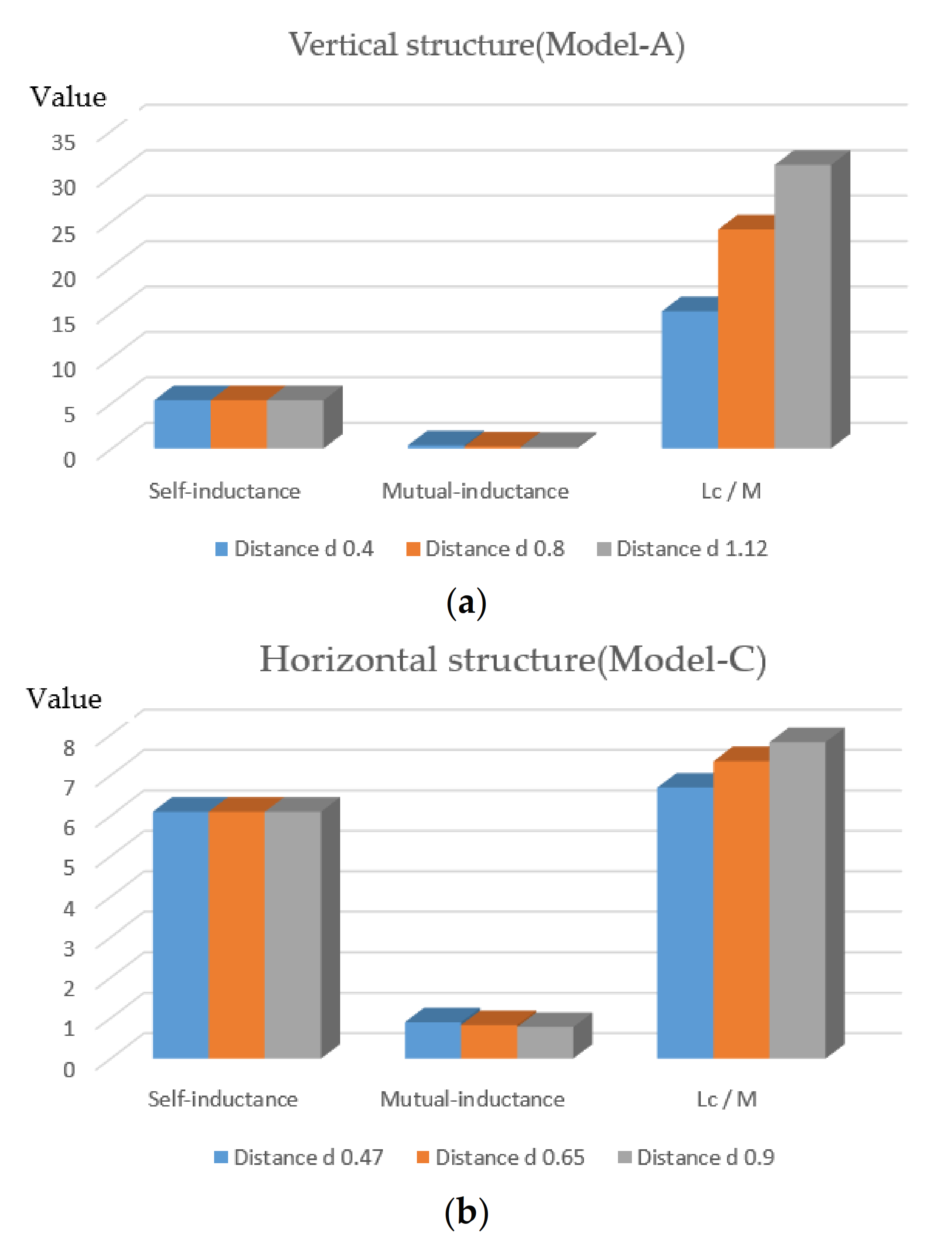
3.2. Magnetic Flux Incident Area

Figure 6 and Table 2 presents the analysis results of the influence between the coil and conductor according to the area of the surface where the magnetic flux is incident in the coil, and the finite element analysis was conducted based on the PCB layout. Moreover, it includes the results of analyzing the mutual inductance of the coil and the self- inductance of the coil according to the incident area in the vertical coil structure and horizontal coil structures. In the vertical coil on the PCB, the magnetic flux incident area of the coil was determined by the number of layers from the bottom layer, whereas in the case of the horizontal coil, it can be set in various ways by the designer with a high degree of freedom. In addition, the distance between the coil and the trace was fixed to 0.47 mm to see only the influence of the change on the magnetic flux incident area.
The results in Table 2 show that the amount of magnetic flux passing through the magnetic flux incident surface increases as the coil width increases, and the mutual inductance value increases accordingly; this demonstrates that the amount of change in the incident magnetic flux is determined according to the size of the incident area. Moreover, the Lc/M value for the horizontal coil (Model-C) is less than that for the vertical coil (Model-A), i.e., it can be seen that the mutual inductance value between the coil and conductor increases based on the same self-inductance value. Therefore, to increase the mutual inductance value to increase the sensor sensitivity for a specific bandwidth, an appropriate magnetic flux incident area through which the magnetic flux passes must be selected.

3.3. Distance between Conductor and Coil
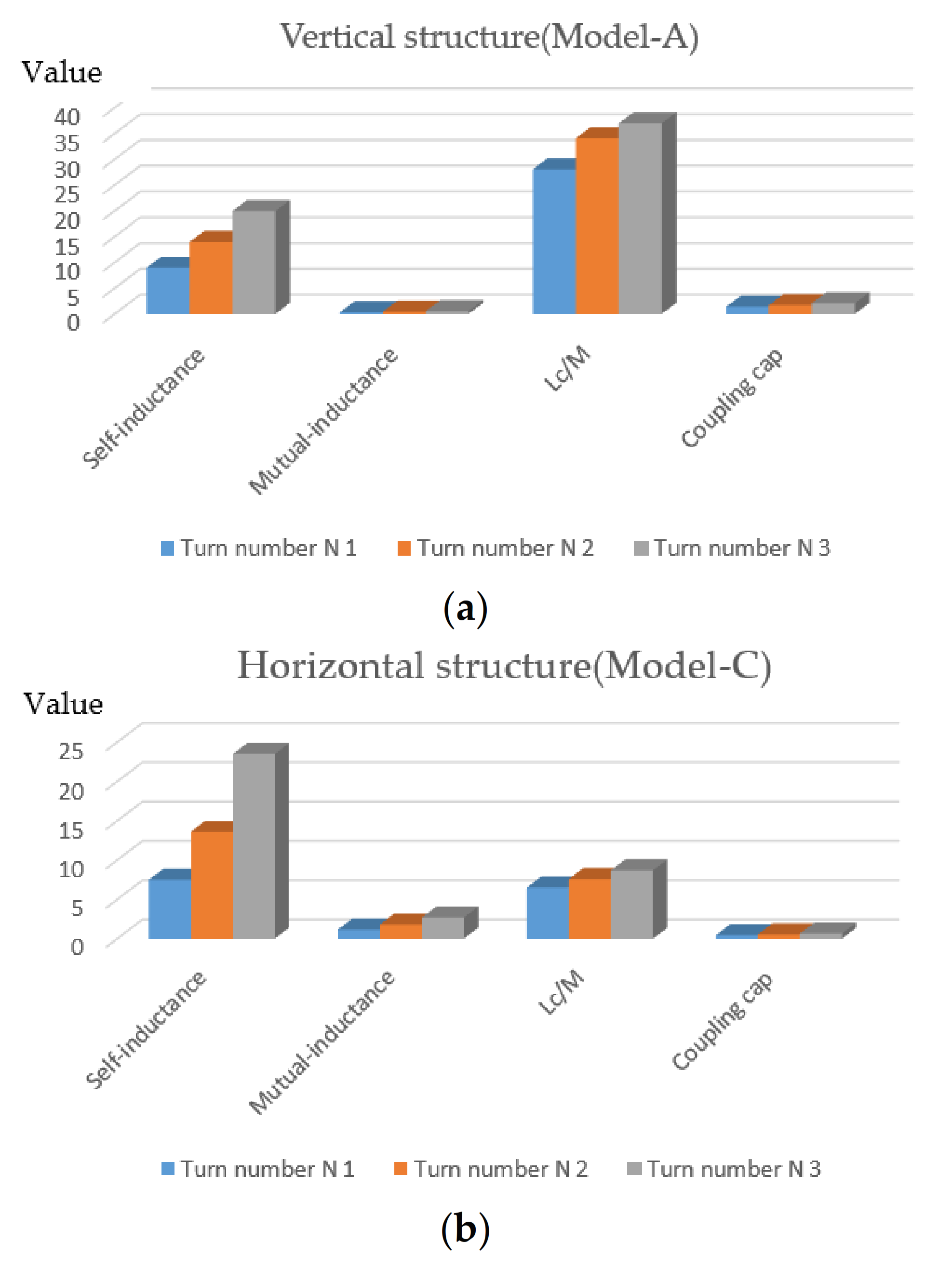
Figure 7 and Table 3 presents the FEM results of mutual inductance and inductive coupling index according to the distance between the coils (Model-A and Model-C) and the conductor through which the primary current flows. From the results of both structures, it is confirmed that the Lc/M of the coil increased as the distance between the coil and the conductor increased in the two coil models in the given d range. In the vertical structure, d is determined as much as the height of the layer; hence, the range that can be varied is limited.
A pickup coil is a typical non-contact insulation sensor, but the coupling noisecurrent affects the sensor coil owing to the coupling capacitance, Ccoup, between conductors formed by the close distance between the conductor and sensor coil. In this case, particularly for a WBG device such as a GaN semiconductor, which has a high dv/dt characteristic, the sensitivity of coupling noise in the power semiconductor affects the sensor coil during switch operation, hence the overshoot or ringing phenomena due to noise can occur at the coil output.
i c = C c o u p d d t v e x t ( t )
where uext is the voltage gradient of the drain to source voltage of the power semiconductor, ic is the coupling current in the pickup coil, and ve is EMF of the coil and the arrows on the circuit show the flow of the coupling noise current.
Figure 8 shows the sensor coil equivalent circuit, considering the formation of the coupling capacitance [23]. In the coil output stage, the original coil EMF vcoil and the voltage to which the voltage drops due to coupling noise vcoup is added.
v o = v c o i l + v c o u p
Figure 9 and Table 4 presents the results of analyzing the influence of the coupling capacitance according to the distance between the pickup coil and the conductor and through which the primary current flows, using the finite element method. From the Table 4 results, it was confirmed that the smaller d, the larger the value of the coupling capacitance in the two coil models, and this shows that it is necessary to consider the coupling noise according to d. Moreover, the value of the coupling capacitance is larger in the vertical structure (Model-A) than in the horizontal structure (Model-C).

3.4. Turn Number

Increasing the number of turns in the pickup coil can increase the sensitivity of the sensor by increasing the mutual inductance between the coil and conductor. As shown in Figure 10, the number of turns of the coil can be implemented through vias in the case of Model-A and a multi-layer coil in the case of Model-C. For a multi-turn coil, the mutual inductance between the coil and the conductor is N times that of a single-turn coil as defined by Equation (20).
M s = N μ o a 2 π ln b + d d
However, the increased self-inductance (Lc) value due to the increased number of turns can reduce the bandwidth of the coil. Therefore, in case of the high-speed power semiconductor devices (such as GaN semiconductor), the accuracy can be decreased when measuring the switch current.
Figure 11 and Table 5 is the result of FEM analysis for Models-A and Models -C, and the spacing between the coils and coils of Models-A and C was unified to 0.4 mm corresponding to the layer thickness. For both coil models, higher values of Lc/M values and coupling capacitance values are observed between the conductors at a higher number of turns.

3.5. External Magnetic Field Interference

Various external current traces can exist in the vertical and horizontal directions around the pickup coil in the PCB, as shown in Figure 8. As the pickup coil A is located inside the PCB as shown in Figure 12, in case the current flows through the external trace located at the distance of x and height y from the pickup coil, the external magnetic flux can pass through the closed-loop area of the coil. Moreover, the magnetic flux is given by Equation (21), and it is added to the amount of original magnetic flux flowing into the magnetic flux incident area of the pickup coil. The total magnetic flux (22) ϕtot is obtained by summing the magnetic flux ϕ1 due to the original current and the magnetic flux ϕext due to the external current.
ϕ e x t = μ o b I 4 π ln 4 x 2 + 2 y + a 2 4 x 2 + 4 y 2
ϕ t o t = ϕ 1 + ϕ e x t 1 + ϕ e x t 2
Accordingly, the voltage at the output stage of the coil is as shown in the following equation, and it affects the mutual inductance and measurement accuracy of the coil.
v t o t = v 1 + v e s t 1 + v e s t 2 + N d ϕ t o t dt = M d i t o t dt
where v1 is the induced voltage due to the original current, and vext is the induced voltage due to the external current.
Therefore, it is necessary to consider the influence of the position of the external conductor in situations in which accurate switch current measurement in case of designing the pickup coil in PCB is required.

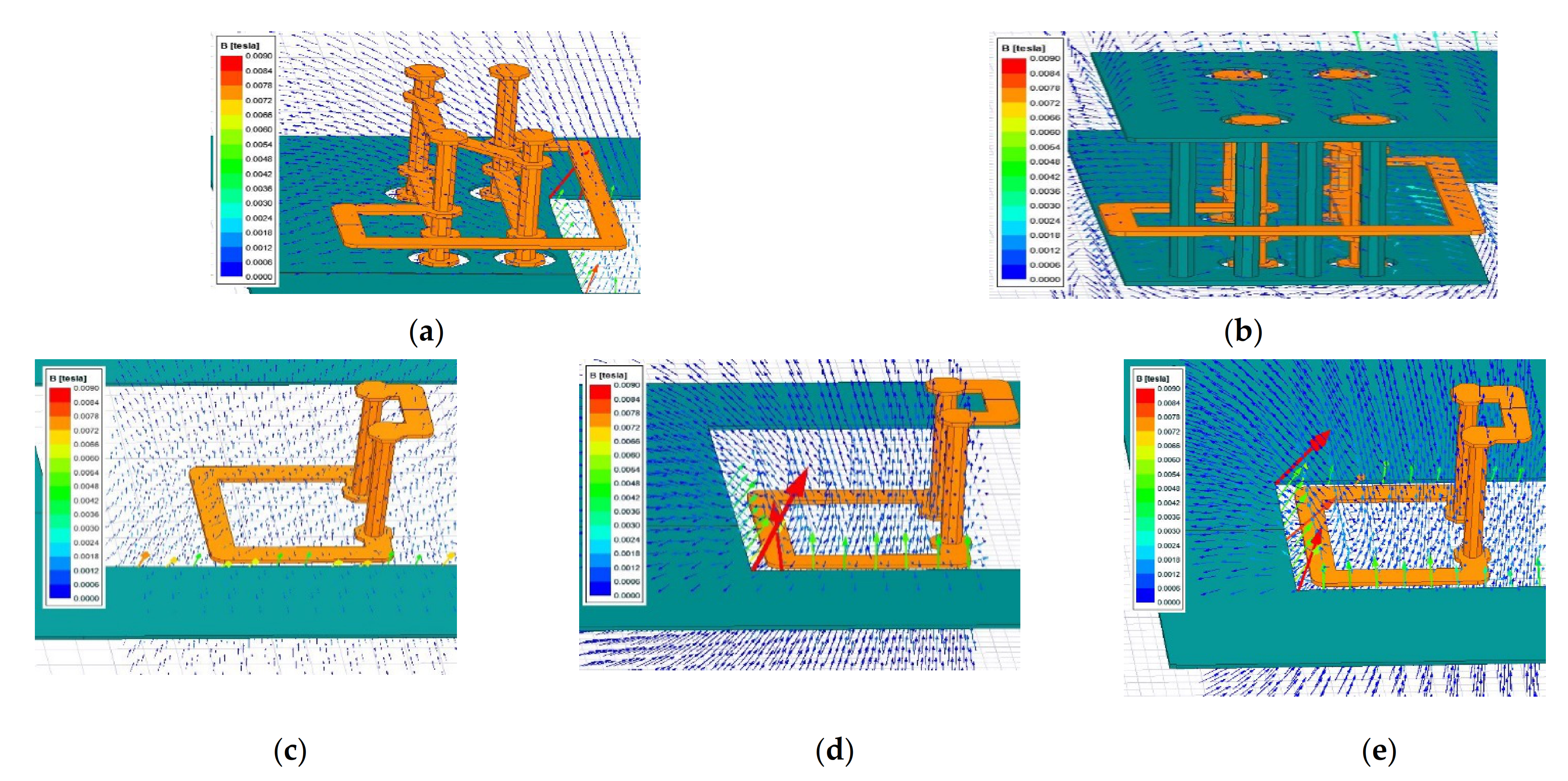
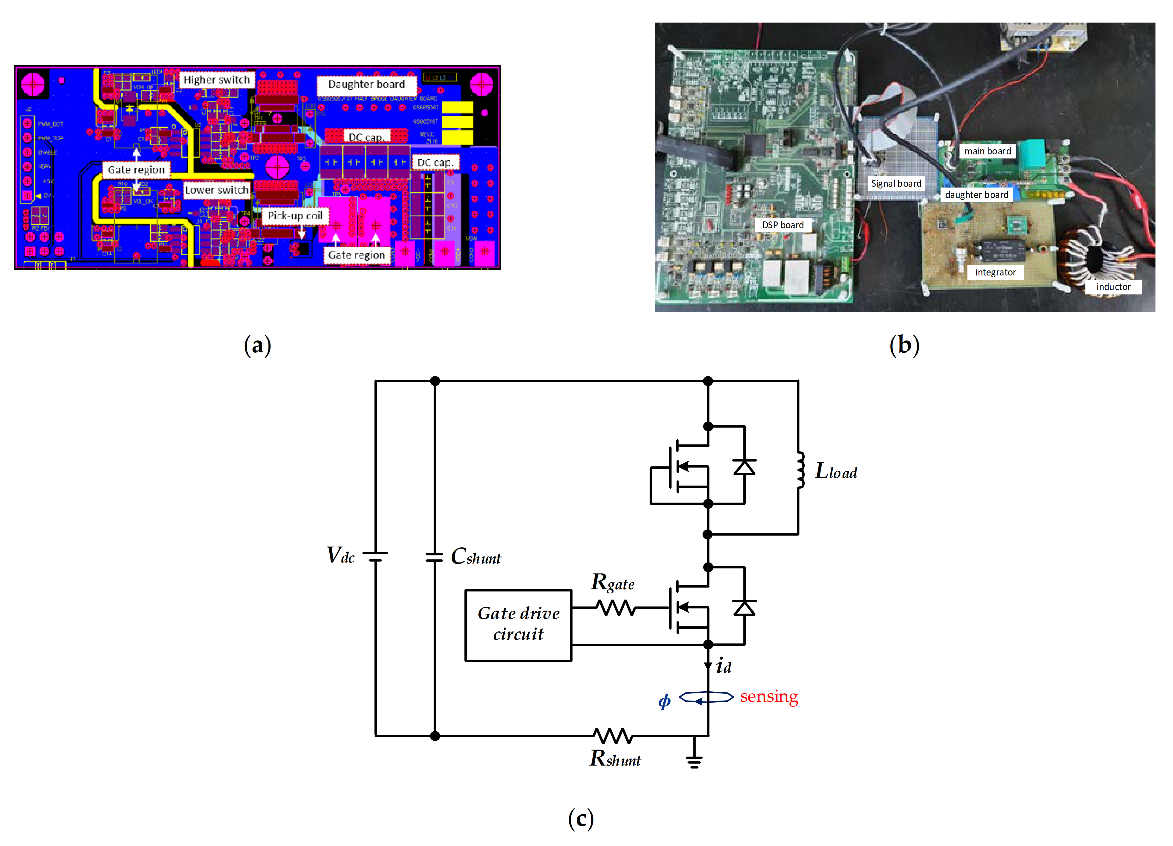
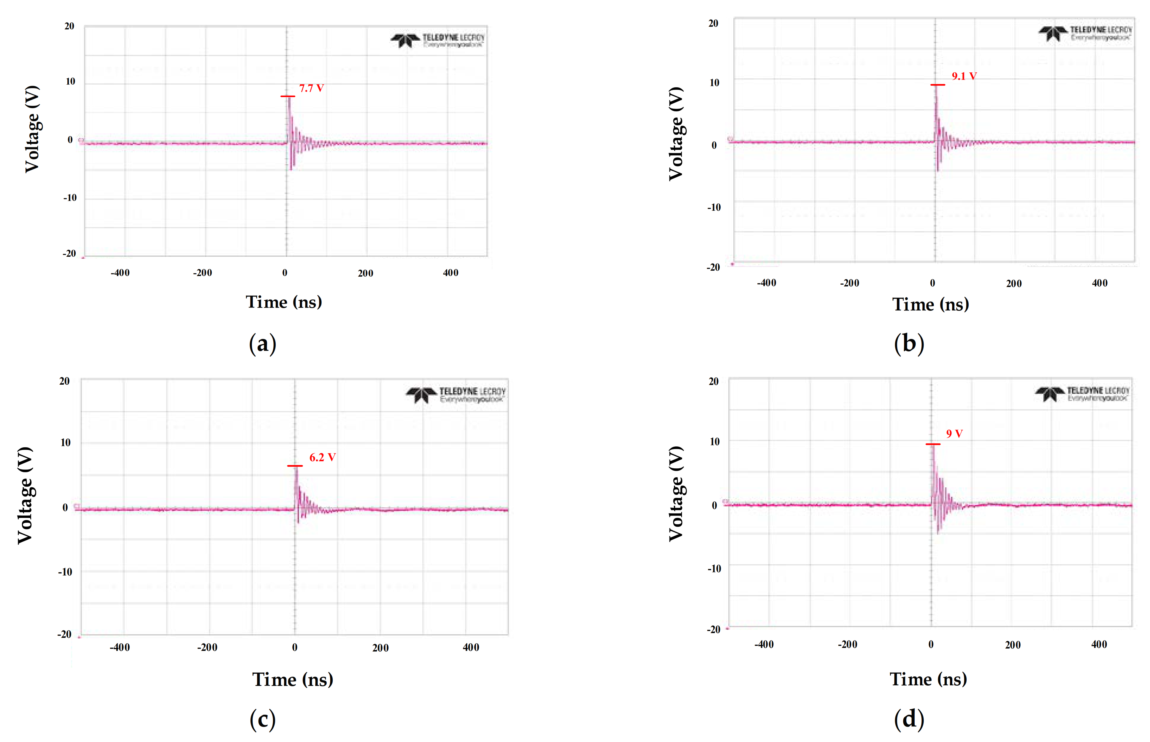
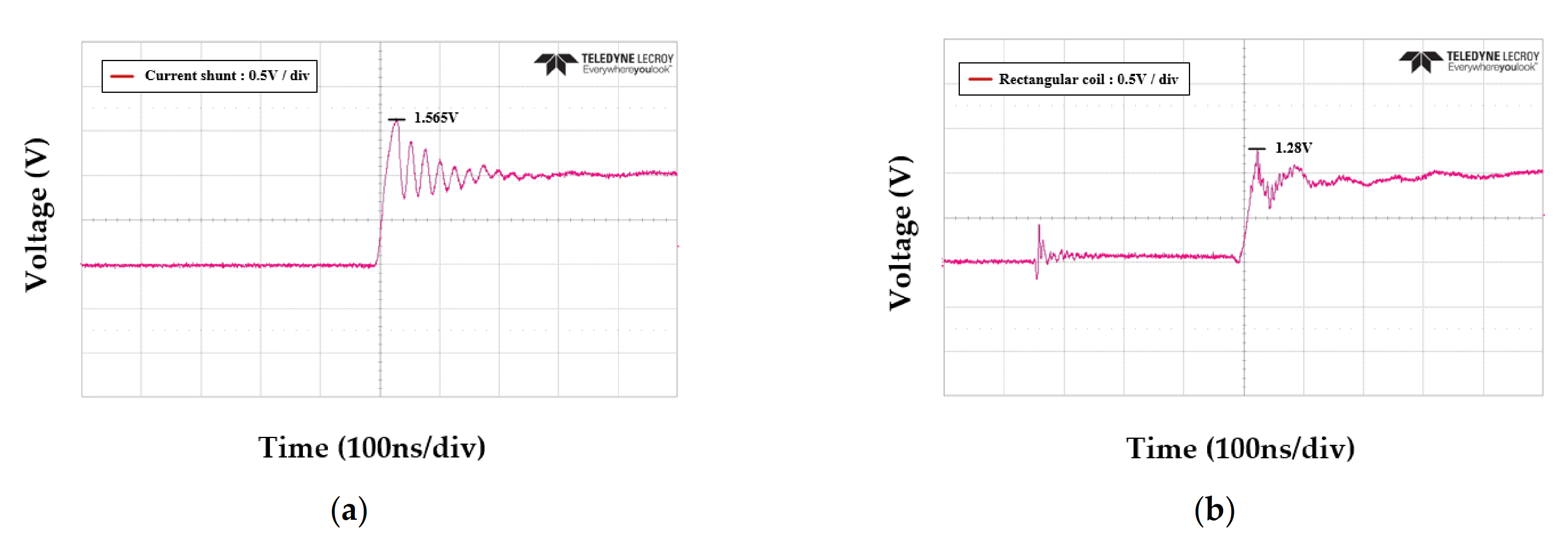
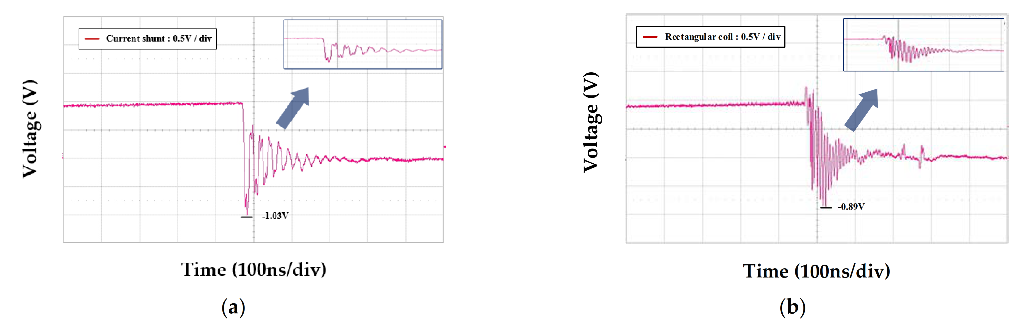
4. Experimental Verification

Figure 13a shows the Gerber file of the daughter board containing information of the GaN-GS66508 T-based, half-bridge circuit and the pickup coil of Model-E described in this paper. This layout is a half-bridge structure for the double pulse test [35], and a pickup coil is configured to measure the primary current flowing on the bottom layer of the PCB. Figure 13b shows the entire double pulse test set, including an active integrator, digital signal processor board, inductor, and mainboard, which is vertically coupled with the daughter board through the connector. Moreover, as a commercial current sensor for comparison and verification with the pickup coil, a shunt resistor sensor was used. The experiment was conducted based on the parameter values of each coil and integrator configuration, as shown in Table 6. In the case of the magnetic flux incident surface, the maximum width allowed in the PCB space was set according to the parameter analysis, and the distance between the coil and the trace was set to an optimum value of 0.65 mm. In the case of the operational amplifier (op-amp) constituting the integrator, LM7171 is manufactured by Texas Instruments, Dallas, Texas, USA with a high slew rate of 4100 V/µs, and the wide unity-gain bandwidth of 200 MHz was selected. Furthermore, Table 7 lists the experimental conditions for the double pulse test circuit (DPT) test.
Figure 14 shows the pickup coil output value without an integrator when the switch is operated in a DC voltage environment of 100 V and 200 V. From the experimental results, the positive peak values of the output values when switched on and off in a 100 V DC voltage environment are 9.1 V and 7.7 V, respectively, and the positive peak values of the output values when switched on and off in a 200 V DC voltage environment are 9 V and 6.2 V, respectively. Therefore, the peak value is generally lower in a DC environment of 200 V than at 100 V, and it is higher in the switch-off period than in the switch-on period.
Figure 15 shows the result of transient response analysis in the switch-on section through a double pulse test. Figure 15a,b are the result of current shunt output, sensor output of rectangular coil, respectively during switch-on. From the experimental results, the peak values during the switch-on operation were 1.56 V, and 1.28 V, respectively, in the order of current shunt and rectangular coil.
In particular, the result of the rectangular coil showed a lower peak value, but a higher noise component was found than the current shunt.
Figure 16 shows the result of transient response analysis in the switch-off section through a double pulse test. Figure 16a,b are the result of current shunt output and sensor output of rectangular coil, respectively, during switch-off. From the experimental results, the peak values during the switch-on operation were 1.03 V and 0.89 V, respectively, in the order of current shunt and rectangular coil. Moreover, similar to the switch-on situation, the result of the rectangular coil showed a lower peak value, but a higher noise component was found than the current shunt.
Therefore, to reduce the occurrence of noise elements in the switch operation of both coils, additional research is needed to reduce the influence of coupling and external noises.

5. Conclusions

This study analyzed various coil parameters related to the configuration of a PCB-embedded pickup coil as a current sensor to measure the switch current of a half-bridge system equipped with a GaN power semiconductor in a discrete package. The analysis was focused on five coil models that could be configured according to the number of conductors located adjacent to the coil, the area of the coil incident surface through which the magnetic flux passes, the distance between the coil and conductor, the number of turns of the coil, and the influence on the presence of an external magnetic flux. FEM was conducted concerning the coil inductance and coupling capacitance, which affect the sensitivity, bandwidth, and noise immunity.
According to the analysis results, in the case of a horizontal direction coil for a conductor through which the primary current flows, a coil with a lower self-inductance value compared to a specific mutual inductance value compared to the conventional pickup coil model vertical coil can be constructed. This shows that a wider bandwidth can be obtained at the same measurement sensitivity in a horizontal direction coil. In addition, the same trend was observed as the ratio of adjacent trace areas to the coil increased. In the case of the incident area of the coil through which the magnetic flux passes, as the value increases, the mutual inductance increases simultaneously due to the increase of the passing magnetic flux, and the ratio of the magnetic inductance to the mutual inductance decreases. However, in the case of the distance between the coil and the conductor, the point where the ratio of mutual inductance to self-inductance is lowest at a specific distance in a horizontal structure was confirmed, and it can be observed that an optimum distance exists according to the characteristics of the current. On the other hand, it was confirmed that the closer the distance between the coil and trace is, the greater the influence on the coupling noise. In the case of the number of coil turns, the ratio of self-inductance to mutual inductance tends to increase as the number of turns increases, and the coupling noise immunity tends to decrease. The experimental verification of the pickup coil was performed by embedding and configuring rectangular coils horizontally located on three traces through which primary currents flow in a half-bridge system using non-modular GaN-based power semiconductors.

Funding

This research received no external funding.

Institutional Review Board Statement

Not applicable.

Informed Consent Statement

Not applicable.

Data Availability Statement

The data presented in this study are available within the article.

Conflicts of Interest

The authors declare no conflict of interest.

References

  1. Hudgins, J.L.; Simin, G.S.; Santi, E.; Khan, M.A. An assessment of wide bandgap semiconductors for power devices. IEEE Trans. Power Electron. 2003, 18, 907–914. [Google Scholar] [CrossRef] [Green Version]
  2. Millán, J.; Godignon, P.; Perpiñà, X.; Pérez-Tomás, A.; Rebollo, J. A survey of wide bandgap power semiconductor devices. IEEE Trans. Power Electron. 2013, 29, 2155–2163. [Google Scholar] [CrossRef]
  3. Biswas, S.; Reusch, D.; de Rooij, M.; Neville, T. Evaluation of measurement techniques for high-speed GaN transistors. In Proceedings of the 2017 IEEE 5th Workshop on Wide Bandgap Power Devices and Applications (WiPDA), Albuquerque, NM, USA, 30 October–1 November 2017; IEEE: New York, NY, USA, 2017. [Google Scholar] [CrossRef]
  4. Huang, B.; Li, Y.; Zheng, T.Q.; Zhang, Y. Design of overcurrent protection circuit for GaN HEMT. In Proceedings of the 2014 IEEE Energy Conversion Congress and Exposition (ECCE), Pittsburgh, PA, USA, 14–18 September 2014; IEEE: New York, NY, USA, 2014. [Google Scholar] [CrossRef]
  5. Wang, K.; Yang, X.; Li, H.; Ma, H.; Zeng, X.; Chen, W. An analytical switching process model of low-voltage eGaN HEMTs for loss calculation. IEEE Trans. Power Electron. 2015, 31, 635–647. [Google Scholar] [CrossRef]
  6. Jones, E.A.; Wang, F.; Costinett, D.; Zhang, Z.; Guo, B.; Liu, B.; Ren, R. Characterization of an enhancement-mode 650-V GaN HFET. In Proceedings of the 2015 IEEE Energy Conversion Congress and Exposition (ECCE), Montreal, QC, Canada, 20–24 September 2015; IEEE: New York, NY, USA, 2015. [Google Scholar] [CrossRef]
  7. Ziegler, S.; Woodward, R.C.; Iu, H.H.C.; Borle, L.J. Current sensing techniques: A review. IEEE Sens. J. 2009, 9, 354–376. [Google Scholar] [CrossRef]
  8. Xiao, C.; Zhao, L.; Asada, T.; Odendaal, W.G.; Van Wyk, J.D. An overview of integratable current sensor technologies. In Proceedings of the 38th IAS Annual Meeting on Conference Record of the Industry Applications Conference, Salt Lake City, UT, USA, 12–16 October 2003; IEEE: New York, NY, USA, 2003; Volume 2. [Google Scholar]
  9. Samimi, M.H.; Mahari, A.; Farahnakian, M.A.; Mohseni, H. The Rogowski coil principles and applications: A review. IEEE Sens. J. 2014, 15, 651–658. [Google Scholar] [CrossRef]
  10. Shepard, D.E.; Donald, W.Y. An Overview of Rogowski Coil Current Sensing Technology; LEM DynAmp Inc.: Grove City, OH, USA, 2000. [Google Scholar]
  11. Quercia, A.; Albanese, R.; Fresa, R.; Minucci, S.; Arshad, S.; Vayakis, G. Performance analysis of Rogowski coils and the measurement of the total toroidal current in the ITER machine. Nucl. Fusion 2017, 57, 126049. [Google Scholar] [CrossRef] [Green Version]
  12. Koga, M.; Tsukuda, M.; Nakashima, K.; Omura, I. Application-specific micro Rogowski coil for power modules-Design tool, novel coil pattern and demonstration. In Proceedings of the CIPS 2016 9th International Conference on Integrated Power Electronics Systems, Nuremberg, Germany, 8–10 March 2016; VDE: Berlin, Germany, 2016. [Google Scholar]
  13. Marracci, M.; Tellini, B. Design of Accurate Rogowski Coil for High Transient Currents. In Proceedings of the 2019 IEEE International Instrumentation and Measurement Technology Conference (I2MTC), Auckland, New Zealand, 20–23 May 2019; IEEE: New York, NY, USA, 2019. [Google Scholar] [CrossRef]
  14. Ferkovic, L.; Damir, I.; Roman, M. Mutual inductance of a precise Rogowski coil in dependence of the position of primary conductor. IEEE Trans. Instrum. Meas. 2008, 58, 122–128. [Google Scholar] [CrossRef]
  15. Wang, C.; Chen, Y.; Zhang, G.; Zhou, Z. Design of printed-circuit board Rogowski coil for highly accurate current measurement. In Proceedings of the 2007 International Conference on Mechatronics and Automation, Harbin, China, 5–8 August 2007; IEEE: New York, NY, USA, 2007. [Google Scholar] [CrossRef]
  16. Gerber, D.; Guillod, T.; Biela, J. IGBT gate-drive with PCB Rogowski coil for improved short circuit detection and current turn-off capability. In Proceedings of the 2011 IEEE Pulsed Power Conference, Chicago, IL, USA, 19–23 June 2011; IEEE: New York, NY, USA, 2011. [Google Scholar] [CrossRef]
  17. Wang, J.; Shen, Z.; Burgos, R.; Boroyevich, D. Design of a high-bandwidth Rogowski current sensor for gate-drive shortcircuit protection of 1.7 kV SiC MOSFET power modules. In Proceedings of the 2015 IEEE 3rd Workshop on Wide Bandgap Power Devices and Applications (WiPDA), Blacksburg, VA, USA, 2–4 November 2015; IEEE: New York, NY, USA, 2015. [Google Scholar] [CrossRef]
  18. Wang, J.; Shen, Z.; DiMarino, C.; Burgos, R.; Boroyevich, D. Gate driver design for 1.7 kV SiC MOSFET module with Rogowski current sensor for shortcircuit protection. In Proceedings of the 2016 IEEE Applied Power Electronics Conference and Exposition (APEC), Long Beach, CA, USA, 20–24 March 2016; IEEE: New York, NY, USA, 2016. [Google Scholar] [CrossRef]
  19. Wang, J.; Shen, Z.; Burgos, R.; Boroyevich, D. Integrated switch current sensor for shortcircuit protection and current control of 1.7-kV SiC MOSFET modules. In Proceedings of the 2016 IEEE Energy Conversion Congress and Exposition (ECCE), Milwaukee, WI, USA, 18–22 September 2016; IEEE: New York, NY, USA, 2016. [Google Scholar] [CrossRef]
  20. Mocevic, S.; Wang, J.; Burgos, R.; Boroyevich, D.; Stancu, C.; Jaksic, M.; Peaslee, B. Comparison between desaturation sensing and Rogowski coil current sensing for shortcircuit protection of 1.2 kV, 300 A SiC MOSFET module. In Proceedings of the 2018 IEEE Applied Power Electronics Conference and Exposition (APEC), San Antonio, TX, USA, 4–8 March 2018; IEEE: New York, NY, USA, 2018. [Google Scholar] [CrossRef]
  21. Tsukuda, M.; Koga, M.; Nakashima, K.; Omura, I. Micro PCB Rogowski coil for current monitoring and protection of high voltage power modules. Microelectron. Reliab. 2016, 64, 479–483. [Google Scholar] [CrossRef]
  22. Gerber, D.; Guillod, T.; Leutwyler, R.; Biela, J. Gate unit with improved short-circuit detection and turn-off capability for 4.5-kV press-pack IGBTs operated at 4-kA pulse current. IEEE Plasma Sci. 2013, 41, 2641–2648. [Google Scholar] [CrossRef]
  23. Hain, S.; Bakran, M. New Rogowski coil design with a high DV/DT immunity and high bandwidth. In Proceedings of the 2013 15th European Conference on Power Electronics and Applications (EPE), Lille, France, 2–6 September 2013; IEEE: New York, NY, USA, 2013. [Google Scholar] [CrossRef]
  24. Kojovic, L.A. Advanced protection solutions for improved power system dynamics performance. In Proceedings of the IEEE PES Power Systems Conference and Exposition, New York, NY, USA, 10–13 October 2004; IEEE: New York, NY, USA, 2004. [Google Scholar]
  25. Liu, Y.; Xie, X.; Hu, Y.; Qian, Y.; Sheng, G.; Jiang, X. A novel transient fault current sensor based on the PCB Rogowski coil for overhead transmission lines. Sensors 2016, 16, 742. [Google Scholar] [CrossRef] [PubMed]
  26. Parkhideh, B.; Shahriar, J.N. Hybrid magnetoresistor-planar Rogowski current sensing scheme with folded trace magnetic field concentration technique. IEEE Sens. J. 2017, 16, 3446–3452. [Google Scholar] [CrossRef]
  27. Metwally, I.A. New side-looking Rogowski coil sensor for measuring large-magnitude fast impulse currents. Sens. Imaging 2015, 16, 100. [Google Scholar] [CrossRef]
  28. Metwally, I.A. Novel designs of wideband Rogowski coils for high pulsed current measurement. IET Sci. Meas. Technol. 2014, 8, 9–16. [Google Scholar] [CrossRef]
  29. Guillod, T.; Gerber, D.; Biela, J.; Muesing, A. Design of a PCB Rogowski Coil based on the PEEC Method. In Proceedings of the 2012 7th International Conference on Integrated Power Electronics Systems (CIPS), Nuremberg, Germany, 6–8 March 2012; IEEE: New York, NY, USA, 2012. [Google Scholar]
  30. Xue, Y.; Lu, J.; Wang, Z.; Tolbert, L.M.; Blalock, B.J.; Wang, F. A compact planar Rogowski coil current sensor for active current balancing of parallel-connected silicon carbide MOSFETs. In Proceedings of the 2014 IEEE Energy Conversion Congress and Exposition (ECCE), Pittsburgh, PA, USA, 14–18 September 2014; IEEE: New York, NY, USA, 2014. [Google Scholar] [CrossRef]
  31. Wang, K.; Yang, X.; Li, H.; Wang, L.; Jain, P. A high-bandwidth integrated current measurement for detecting switching current of fast GaN devices. IEEE Trans. Power Electron. 2017, 33, 6199–6210. [Google Scholar] [CrossRef]
  32. Zhao, L.; Van Wyk, J.D.; Odendaal, W.G. Planar embedded pick-up coil sensor for power electronic modules. In Proceedings of the Nineteenth Annual IEEE Applied Power Electronics Conference and Exposition, 2004. APEC’04, Anaheim, CA, USA, 22–26 February 2004; IEEE: New York, NY, USA, 2004; Volume 2. [Google Scholar]
  33. Yoshikazu, K.; Wada, K.; Guichon, J.M.; Schanen, J.L.; Roudet, J. Bus bar embedded rogowski coil. In Proceedings of the 2018 IEEE Applied Power Electronics Conference and Exposition (APEC), San Antonio, TX, USA, 4–8 March 2018; IEEE: New York, NY, USA, 2018. [Google Scholar]
  34. Ui-Jin, K.; Kim, R. Analysis of Various Pickup Coil Designs in Nonmodule-Type GaN Power Semiconductors. Sensors 2020, 20, 6066. [Google Scholar]
  35. Ahmad, S.S.; Narayanan, G. Double pulse test based switching characterization of SiC MOSFET. In Proceedings of the 2017 National Power Electronics Conference (NPEC), Pune, India, 18–20 December 2017; IEEE: New York, NY, USA, 2017. [Google Scholar]
Figure 1. Schematic of the pickup coil in PCB: (a) vertical structure and (b) horizontal structure.
Applsci 11 02290 g001
Figure 2. Lumped circuit of the pickup coil.
Applsci 11 02290 g002
Figure 3. Geometry of (a) Model-A: vertical structure of a pickup coil with conductor trace on one side; (b) Model-B: vertical structure of a pickup coil with conductor trace on two sides; (c) Model-C: horizontal structure of a pickup coil with conductor trace on one side; (d) Model-D: horizontal structure of a pickup coil with conductor trace on two sides; and (e) Model-E: horizontal structure of a pickup coil with conductor trace on three sides.
Applsci 11 02290 g003
Figure 4. Magnetic field flux density at 5-A conductor current with finite element method (FEM). (a) Model-A, (b) Model-B, (c) Model-C, (d) Model-D, and (e) Model-E.
Applsci 11 02290 g004
Figure 5. Comparison for the five models. (a) FEM results under different coil configurations and (b) error value of M between calculation results and FEA results.
Applsci 11 02290 g005
Figure 6. FEM results under magnetic flux incident in different areas: (a) vertical structure coil model and (b) horizontal structure coil model.
Applsci 11 02290 g006
Figure 7. FEM results under different distances: (a) vertical structure coil model and (b) horizontal structure coil model.
Applsci 11 02290 g007
Figure 8. Equivalent circuit of a pickup coil with coupling capacitive interferences.
Applsci 11 02290 g008
Figure 9. FEM results of coupling capacitance under different distances: (a) vertical structure coil model and (b) horizontal structure coil model.
Applsci 11 02290 g009
Figure 10. Geometry of the pickup coil with N-turns: (a) vertical structure and (b) horizontal structure.
Applsci 11 02290 g010
Figure 11. FEM results under different turn-numbers: (a) vertical structure coil model and (b) horizontal structure coil model.
Applsci 11 02290 g011
Figure 12. Interference of the external conductor perpendicular to the sensor coil.
Applsci 11 02290 g012
Figure 13. Double pulse test set: (a) Gerber file of the daughter board containing the pickup coil, (b) overall test board, and (c) double pulse test circuit (DPT).
Applsci 11 02290 g013
Figure 14. Measured output of a pickup coil following switch behavior: (a) switch-on condition at 100 V DC voltage, (b) switch-off condition at 100 V DC voltage, (c) switch-on condition at 200 V DC, and (d) switch-off condition at 200 V DC voltage.
Applsci 11 02290 g014
Figure 15. Integrator output waveforms during switch turn-on of pickup coils and shunt resistor sensor at DC link voltage Vdc of 250 V: (a) switch-on condition and (b) switch-off condition.
Applsci 11 02290 g015
Figure 16. Integrator output waveforms during switch turn-off of pickup coils and shunt resistor sensor at DC link voltage Vdc of 250 V: (a) switch-on condition and (b) switch-off condition.
Applsci 11 02290 g016
Table 1. Comparison of the dependent coil structures using finite element method with the FEA method.
Coil ModelModel-AModel-BModel-CModel-DModel-E
Inductive coupling0.030.140.110.1470.2
Self-inductance Ls [nH]5.85.86.486.496.48
Mutual-inductance M [nH]0.420.711.041.31.7
Trace inductance [nH]8.328.656.296.326.41
Lc/M13.88.166.234.993.8
Table 2. Influence of the inductance under different magnetic flux incident areas S with the FEA method.
Coil TypeVertical Structure (Model-A)Horizontal Structure (Model-C)
a × b
(mm × mm)
3.25 × 0.43.25 × 0.83.25 × 1.23.25 × 1.62.92 × 2.182.92 × 3.22.92 × 3.952.92 × 4.63
Area S
(mm2)
1.32.63.95.26.369.3411.513.5
Inductive coupling0.0090.020.0340.0370.090.1290.1550.174
Mutual
inductance M [nH]
0.280.380.450.580.91.351.752.01
Self
inductance Ls [nH]
4.515.175.716.586.297.628.699.63
Lc/M16.11512.611.36.95.64.964.81
Table 3. Influence of the inductance under different distances d with the FEA method.
Coil TypeVertical Structure (Model-A)Horizontal Structure (Model-C)
Distance d
(mm)
0.40.81.120.470.650.9
Inductive coupling0.020.0090.0010.120.110.1
Mutual
inductance M [nH]
0.350.220.170.90.830.78
Self
inductance Lc [nH]
5.315.315.316.16.16.1
Lc/M15.124.131.26.77.357.82
Table 4. Influence of the coupling capacitance under different distances d with the FEA method.
Coil TypeVertical Structure (Model-A)Horizontal Structure (Model-C)
Distance d
(mm)
0.40.81.121.160.470.650.91.12
Coupling
capacitance [pF]
1.080.910.860.830.470.460.430.42
Table 5. Influence under different turn-numbers with the FEM.
Coil TypeVertical Structure (Model-A)Horizontal Structure (Model-C)
Turn number N123123
Mutual
inductance M [nH]
0.320.410.531.151.792.7
Self
inductance Lc [nH]
914207.513.623.5
Lc/M28.134.1376.527.598.7
Coupling
capacitance [pF]
1.411.722.090.460.540.65
Table 6. Circuit parameters of the current sensor.
ParameterValues
Mutual Inductance3.2 nH
Self-Inductance20.5 nH
Self-Capacitance5.56 pF
Self-Resistance0.03 Ω
Coupling Capacitance0.69 pF
Magnetic Flux Incident Areas11.7 mm2
Distance between Trace and Coil0.65 mm
Bandwidth590 MHz
Damping Resistance100 Ω
Integrator Resistance70 Ω
Integrator Capacitance470 pF
Table 7. The double pulse test circuit (DPT) test conditions for each current sensor.
ParameterShunt ResistorPick-Up Coil
DC voltage250 V250 V
Test current±25 A±25 A
Gate Resistance110 Ω110 Ω
Gain0.10.1
Publisher’s Note: MDPI stays neutral with regard to jurisdictional claims in published maps and institutional affiliations.

