Article

Design and Implementation Scheme of QSFP28 Optical Transceiver for Long-Reach Transmission Using PAM4 Modulation †

1
ICT Convergence Research Center, Kumoh National Institute of Technology, Gumi 39177, Gyeongbuk, Korea
2
Department of IT Convergence Engineering, Kumoh National Institute of Technology, Gumi 39177, Gyeongbuk, Korea
3
Coset Inc., PyeongChang 2321, Gangwon, Korea
*
Author to whom correspondence should be addressed.
Fabrication of 53 Gb/s Optical Transceiver over 40-km transmission with PAM4 modulation. In Proceedings of the 2019 21st International Conference on Advanded Communication Technology (ICACT), PyeongChang, Korea, 17–20 February 2019.
These authors contributed equally to this work.
Appl. Sci. 2021, 11(6), 2803; https://doi.org/10.3390/app11062803
Submission received: 2 February 2021 / Revised: 10 March 2021 / Accepted: 16 March 2021 / Published: 21 March 2021
(This article belongs to the Section Optics and Lasers)

Abstract

:
A quad, small form-factor pluggable 28 Gbps optical transceiver design scheme is proposed. It is capable of transmitting 50 Gbps of data up to a distance of 40 km using modulation signals with a level-four pulse-amplitude. The proposed scheme is designed using a combination of electro-absorption-modulated lasers, transmitter optical sub-assembly, low-cost positive-intrinsic-native photodiodes, and receiver optical sub-assembly to achieve standard performance and low cost. Moreover, the hardware and firmware design schemes to implement the optical transceiver are presented. The results confirm the effectiveness of the proposed scheme and the performance of the manufactured optical transceiver, thereby confirming its applicability to real industrial sites.

1. Introduction

Recent, new technologies, such as fifth-generation wireless networks (5G), artificial intelligence (AI), virtual reality (VR), the Internet of things (IoT), and self-driving cars, require a large bandwidth and fast response time. To support the needs of such new technologies, the core network is evolving from 100 GE to 400 GE and the research and development of 400 Gbps optical transceivers continues to progress [1]. With increased data consumption, increased bandwidth is required. For this purpose, long-distance optical transceivers that use a variety of modulation methods such as polarization-multiplexing and quadrature phase-shift-keying (PM-QPSK or DP-QPSK), and quadrant amplitude modulation (QAM) [2] have been developed. However, this modulation method requires an expensive photomultiplier and the corresponding sophisticated technology. A commonly used non-return-to-zero (NRZ) modulation scheme can transmit one bit per symbol. A level-four pulse-amplitude modulation (PAM4) is advantageous because it can transmit two bits per symbol, twice that of the traditional NRZ [3]. However, the PAM4 scheme has a characteristic lower bit error rate (BER) because it is more noise-sensitive than the NRZ method. Therefore, increased caution is required when designing optical transceivers using PAM4.
The Institute of Electrical and Electronics Engineers(IEEE) 802.3 cd standard document defines the physical layer and associated parameter management of 50 Gbps PAM4 optical transmitters and receivers for 50GBASE(Gb/s PHYs)-FR (far reach, 2 km) and LR (long reach, 10 km) [4]. However, the specification for the longest-distance transmission, which is 40 km for PAM4 signals, has been proposed for some enterprises but have yet to be established as a standard [5].
Table 1 shows the existing optical receiver solutions for long-distance transmission. Experiments were conducted using an avalanche photodiode (APD) optical receiver for 40 and 60 km long-distance PAM4 signal transmissions [6,7,8]. However, the method using APD receivers requires additional circuitry to drive the APD and the cost of parts is higher than that of positive-intrinsic-negative photo diode (PIN-PD) receivers. The semiconductor optical amplifier (SOA) is another technology that can be used for long-distance transmissions greater than 40 km [9,10]. SOA has been applied to the C form-factor pluggable (CFP), specifically the CFP2 optical transceiver, which is a large form-factor type owing to the high cost of parts, the additional thermoelectric cooler (TEC) control, and its slarge size; however, it can amplify the optical signal to be lower than the APD method to the level of the receiver sensitivity. These existing studies have successfully long-distance transfers but have not experimented with packaged transceiver types. The study in [11] proposed a method for transmitting long distances using a QSFP28-type transceiver. However, it used a method to amplify signals outside the transceiver by adding the erbium-doped fiber amplifier (EDFA) to the transmission system rather than inside the transceiver.
We designed and implemented the QSFP28 optical transceiver using PAM4. This study makes the following contributions: (1) 50 Gbps high-capacity long-distance transmission, only PIN-PD was used to minimize circuit complexity and was implemented at low cost over traditional approaches. To overcome the limitations of the PIN-PD receiver, the PAM4 signal transmitter output BER was minimized to demonstrate that 40 km transmission is feasible. (2) A hardware and firmware design scheme in which the optical transceiver’s function and performance meet standard specifications is proposed. The optical transceiver manufacturers do not publicly share their methodology or techniques. By implementing optical transceiver using the proposed design scheme, quality can be ensured, and cost and development time can be reduced.
The rest of the paper is organized as follows: In Section 2, the principle of the PAM4 method and the relevant standard are analyzed for the design of the QSFP28 optical transceiver. Section 3 proposes the hardware and firmware design scheme of the QSFP28 optical transceiver based on the analyzed requirements. Section 4 analyzes the test bed construction and test results for performance verification. Section 5 discusses the conclusions and future studies.

2. Related Work

This section analyzes the relevant standards and describes the PAM4 technology and the QSFP28 optical transceiver design requirements.

2.1. PAM4

Improved modulation methods are attempted owing to the increase in data demand. The NRZ-type modulation scheme has been most commonly used in data transmission. Meanwhile, the PAM4 scheme was attempted by a company that created the digital signal processing (DSP) integrated circuit (IC) for data modulation [12]. Figure 1. shows a comparison between the NRZ and PAM4 signals. Compared with NRZ, PAM4 demonstrates numerous benefits associated with having half the Nyquist frequency. These benefits include doubling the data density, achieving higher resolution using the same oversampling rate, and having the same total noise power spread over a wider frequency band.
The NRZ modulation scheme encodes a binary pattern, such as 0110010, into a continuous sequence of fixed voltage levels of low and high voltages of 0 and 1, respectively. Assuming a bit rate of 25 Gbps, faster bit speeds and higher bandwidths are needed to transmit 50 Gbps, which is twice the bit rate. To double the bit rate without doubling the bandwidth, the signal level must be split in half and added to the signal. Thus, there are four signal levels, similar to that of the PAM4 signal, and 2 bits per level symbol is assigned. Meanwhile, the IEEE P802.3bj KP4 standard defines the requirements for 28 Gbps PAM4 signals, whereas the IEEE P802.3bs andOptical Internetworking forum(OIF) CEI-56G-PAM4 documents define standards for 56 Gbps PAM4 signals [13,14].

2.2. QSFP28 Optical Transceiver Hardware Standard

The QSFP28 optical transceiver complies with the QSFP multi-source agreement (QSFP-MSA) specification. SFF-8665 is a standard document for QSFP28 optical transceiver solutions [15]. The QSFP28 specification documents to be referenced for the manufacture of optical transceivers consist of documents on the electrical characteristics of optical transceivers, instrument specifications such as optical transceiver connectors and sizes, cage specifications on the host side to operate with inserted optical transceivers, and management interface specifications that can be viewed as software specifications. The SFF-8679 specification describes the hardware and electrical characteristics that the QSFP28 optical transceiver must fulfill and defines the connector specification for the QSFP28 optical transceiver; the function of each pin; and the interface for the data, control, and status signals of the optical transceiver [16]. In addition, the electronic static discharge (ESD) specification and the instrument-related specifications of the optical transceiver as well as the temperature and timing specifications are defined. Figure 2 shows the QSFP28 optical transceiver and host interface structure proposed in the standard document.
The hardware configuration of the QSFP28 optical transceiver consists of a quad optical transmitter and quad optical receiver for transmission and reception, a clock data recovery (CDR) IC for processing the transmission signals, a micro-controller unit (MCU) for operation of the QSFP28 optical transceiver, and a host connector for sending and receiving control and data signals with the host. There are up to four channels for data transmission and reception. The functions of control and alarm signals are summarized in Table 2. The power consumption of the QSFP28 optical transceiver is divided into eight classes according to the available host system capacity, with each class defining the maximum allowable power. If the optical transceiver’s power consumption exceeds the specified consumption capacity, the QSFP28 optical transceiver is applied with an LPMode signal to enter the low-power state. The QSFP28 optical transceiver in a low-power state should have a power consumption of less than 1.5 W. Another standard document defines temperature specifications for normal operation of the optical transceiver from a minimum of 0 °C to a maximum of 70 °C based on the QSFP28 optical transceiver case. Finally, the timing specification for the response speed of the QSFP28 optical transceiver according to the hardware control signal of the host and the timing specification for alarm generation are defined.

2.3. QSFP28 Optical Transceiver Software Standard

The specifications for the operation and management of QSFP28 optical transceivers are defined in the SFF-8636 document [17]. The QSFP28 optical transceiver uses a 2-wire bus interface to communicate with the host. The 2-wire bus interface for QSFP28 is the same as that used in inter-integrated circuit (I2C) communications but with some differences in the write operation. The 2-wire interface does not support a “combined format” that can send continuous write addressing for writing. Therefore, under repeated start conditions, the firmware should be implemented to discard writing operation and to abort the data received. Figure 3 shows the procedure for a byte write behavior in the I2C interface between the host and the optical transceiver as defined in the standard. Figure 3a is a one-byte write operation, and Figure 3b is a sequential byte write operation. The host system becomes the master, and the QSFP28 optical transceiver is a slave. The I2C interface sends I2C frames in bytes, checks the opponent’s acknowledgement in the ninth clock, and sends/receives additional data in bytes. It should be able to send up to four sequential bytes in a sequential write operation. Detailed procedures for the I2C interface protocol between the QSFP28 optical transceiver and the host are defined in the standard document.
To control the operation of the QSFP28 optical transceiver through the host interface and to check the optical transceiver status, the QSFP28 optical transceiver configures the internal register map. Figure 4 shows the register map structure defined in the standard. The physical address for accessing the QSFP28 register with the I2C interface is 0 × A0 in hexadecimal. The QSFP28 register consists of pages, and each page consists of 128 bytes. The register consists of one lower page and a number of upper pages, and an upper page consists of a basic required page and an optional page. The address to access the register, lower page, and upper page ranges from 0 × 00 to 0 × FF, from 0 × 00 to 0 × 7F, and from 0 × 80 to 0 × FF, respectively. Data, such as interrupt flags and status monitoring, that require quick access are configured on the lower page for timely access. Page 01 h, corresponding to an upper page, can implement an application option table, and page 02 h acts as an electrically erasable programmable read-only memory (EEPROM) by allowing users to arbitrarily read and write. Pages 20 h to 21 h includes the information from additional monitored parameters for modules that have PAM4 such as alarm and monitoring parameters. This study includes support for additional monitoring parameters for QSFP28 optical transceivers. To access the upper page, The host can read or write the value to the upper page address after writing the upper page index value to access the lower page address 0 × 7F.

3. Proposed Design Scheme

3.1. Hardware Design

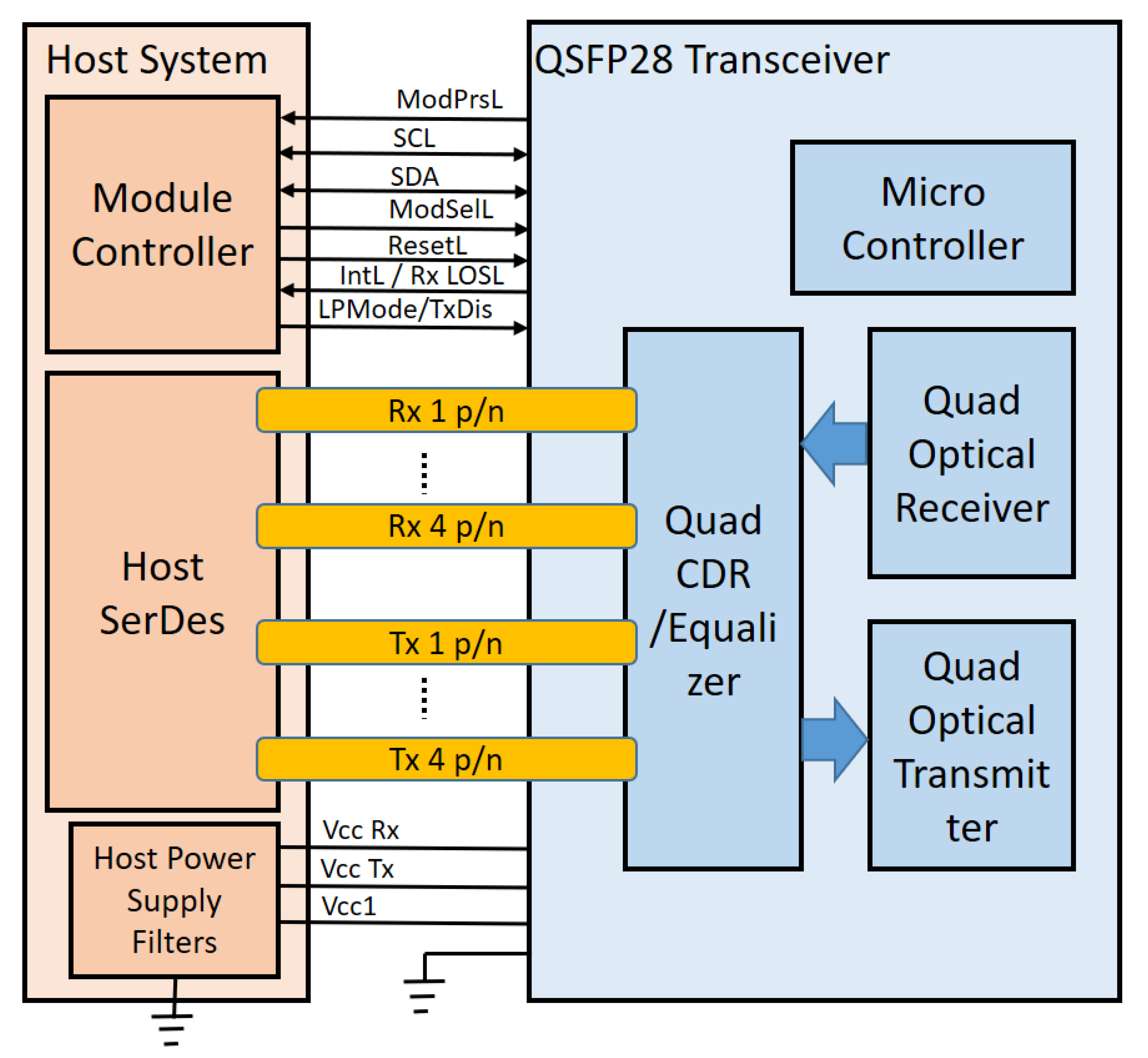
Figure 5 shows the complete hardware structure diagram proposed with reference to the standard documentation. The QSFP28 optical transceiver internal hardware of the proposed design scheme consists of PAM4 DSP IC for PAM4 and duplication, electro-absorption-modulated laser (EML)–transmitter optical sub-assemblies (TOSA) for transmission, and PIN-PD receiver optical sub-assemblies (ROSA) for reception. It also consists of a driver IC for driving one TOSA, a TEC controller for controlling optical transmitters wavelengths, and an MCU for overall operation of modules.
The PAM4 DSP IC functions to modulate two 25 Gbps NRZ signals with 50 Gbps PAM4 signals and, vice versa, that is, to convert PAM4 signals to NRZ signals. The EML-TOSA is a 25/28 G single channel TOSA and applies an electro-absorption modulator and distributed feedback laser diode (DFB-LD), monitor photodiode, embedded optical isolator, and TEC to a gold box-type package. The TEC controller is used to control the TEC inside the TOSA. Because the TOSA laser diode has the characteristic that the wavelength varies according to temperature, the internal TEC controls the laser diode to maintain a constant temperature without being affected by external temperature. The linear PIN-PD ROSA for receiving PAM4 optical signals consists of a photodiode of 25 GHz bandwidth and a trans-impedance amplifier (TIA) capable of receiving up to 2.5 mA inputs and is adjustable from 31 to 37 GHz. The MCU controls laser diodes, linear drivers, and linear TIA using a built-in analog-to-digital converter (ADC) and digital-to-analog converter (DAC). The MCU is also responsible for operation of the PAM4 DSP IC and operation of the QSFP28 optical transceiver.
For optical transceivers manufactured with the QSFP28 form-factors, a number of ICs must be integrated in a limited printed circuit board (PCB) area. Therefore, we optimized the PCB design by selecting each IC for the QSFP28 design in consideration of its small size and high-efficiency characteristics. In particular, DC–DC converters for power supply are more than 90% efficient and the inductor is applied with switching converters integrated inside the IC to minimize the area. This can reduce the heat in the power supply and lower the power consumption.

3.2. PCB Design

The circuit design proposed in this study was implemented on a 10-layer PCB to optimize the circuit in a limited area. The parameters that determine high-speed signal loss are the dielectric constant (Dk) and the dissipation factor (Df) for frequency. Although PCB material with less Dk and Df has the advantage of less high-frequency loss, its price is higher. Therefore, an appropriate trade-off design is required considering cost and performance. In this study, we used FR4 substrates, which are primarily used for industrial purposes, and Panasonic MEGTRON6 with relatively lower Dks and lower dielectric losses compared to FR4 substrates. The 25 Gbps NRZ high-speed signal and PAM4 signal transmission lines were placed in the top and bottom planes using the MEGTRON6 substrate, and the remainder was designed with FR4 substrates. Table 3 shows the PCB layer structures designed by the proposed method and their circuit functionality implemented on each layer.
The design of the transmission line for transmitting 26 giga-baud (GBd) PAM4 signals per channel over the PCB requires a more sophisticated transmission line design than conventional NRZ signals. The PAM4 signals are more susceptible to noise and attenuation than NRZ signals. A signal passing through a transmission line on a PCB designed with differential 100 Ohms results in reflection or radiation of the signal at the point of the characteristic impedance mismatch, thus impacting the signal characteristics. This causes overshoot and undershoot on the signal eye pattern and degrades jitter properties. The main areas where impedance nonconformities occur are IC pads and the flexible PCB assembly. The proposed scheme is used to apply a coplanar waveguide type transmission line on the PCB. The impedance of the area where the transmission line width thickens increases capacitance, and the dielectric substrate thickness below the transmission line decreases capacitance [18]. The proposed scheme minimizes impedance nonconformity by subtly calculating the impedance characteristics according to the line width, the dielectric thickness, and the gap between the track and the ground (GND) and increases inductance to solve the impedance degradation problem occurring on IC pads on the path through which the signal passes, thereby improving the overall impedance convergence.

3.3. Firmware Design

The QSFP28 optical transceiver firmware design scheme proposed in this study was designed to meet the requirements of standard documents. The DS4830 of Maxim Integrated was used as the MCU for the QSFP28 optical transceiver [19]. The DS4830 supports optimized control for information monitoring of optical transceivers that meet the SFF-8472 standard. It provides ADC and DAC with 12-bit resolution and I2C slave interface that can operate reliably at a 400 kHz clock speed. 
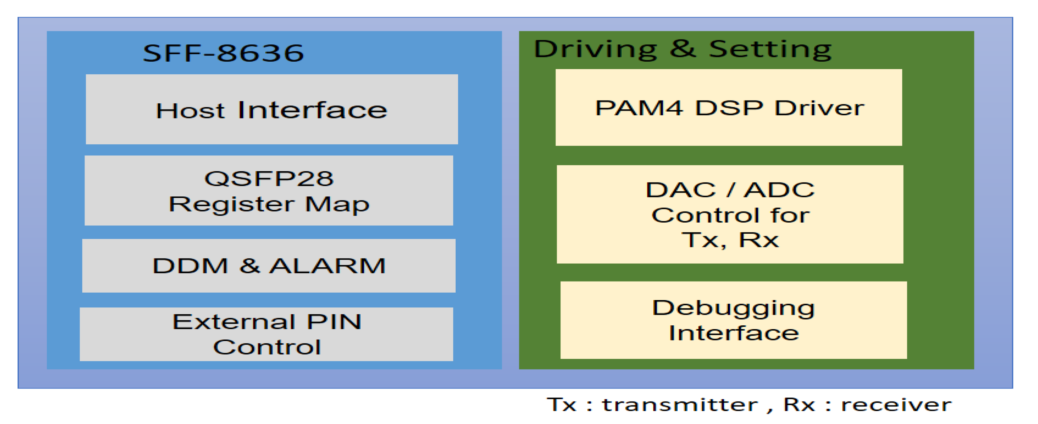
Figure 6 shows the QSFP28 firmware design block diagram.
The QSFP28 optical transceiver defines the internal registers for control and monitoring in the standard and uses I2C as the host access interface. In addition, the firmware implements digital diagnostic monitoring (DDM) and alarm functions to indicate the optical transceiver status and implements external pins functions connected by the connectors described in Section 2. Moreover, the firmware implements the PAM4 DSP IC drive function for PAM4 processing, the DAC control function to drive transmission IC, the ADC control function to update DDM information, and the debugging interface to help debug and set up the optical transceivers. The debugging interface is not directly implemented but is indirectly designed so that the manufacturer’s area of the QSFP28 register is defined and used for debugging purposes.
Figure 7 shows the firmware sequencing of the QSFP28 PAM4 optical transceiver. The operation is initiated when the optical transceiver is energized or the reset signal is released. First, the MCU initializes the peripherals. The peripherals to be used in the proposed scheme are ADC for temperature, drive voltage, and alarm monitoring; DAC to drive the transmitting optical components such as EML-TOSA; I2C slave functions to be used as host interfaces; and I2C master functions to communicate with the external ADC IC and PAM4 DSP IC. Additionally, the Watchdog timer is initialized for firmware stability and for setting up the General-Purpose Input/Output(GPIO) pin. When the MCU peripheral initialization is complete, the PAM4 DSP IC initialization process is followed. To operate the PAM4 DSP IC, the firmware for DSP IC drive must be downloaded and initialized. The ADC IC is added in this scheme for channel scalability and precise measurement. Thus, the operating program undergoes an initialization process to utilize the external ADC IC. In addition, the process of initializing the global variables required for QSFP28 optical transceiver operation is followed by an infinite polling loop. The operating program checks the status of the LPMode/TxDIS pin and, if enabled, switches the PAM4 DSP IC to a non-operational state and shuts off the transmitting optic components power. If both LPMode/TxDIS pins are inactive, it commands the PAM4 DSP IC to drive and proceed with power activation and optimization settings for the transmission photomultiplier. For operation and optimization of the PAM4 DSP IC, the manufacturer’s datasheet was referenced and the API provided by the manufacturer was ported to the MCU to implement the drive driver. Finally, a function related to alarm monitoring was executed so that the optical transceiver status could be constantly monitored. If a monitoring and control request is received from the external host interface, the MCU generates an I2C request interrupt and performs the processing as requested.

QSFP28 Register Configuration and Control Algorithm

As described in Section 2.3, the QSFP28 optical transceiver should define the internal register to receive control and monitoring requests from the host system and should configure nonvolatile registers, such as the upper page 0 × 02 area, at the request of the standard document. The proposed scheme allocates a portion of the MCU’s flash memory to store nonvolatile data. For the host to access the upper page 0 × 02 of the QSFP28 optical transceiver, it must first change the page selection address (0 × 7F) value on the lower page. To implement the page access function, the proposed scheme designates that the MCU uploads the value of the flash memory area of the page to the RAM when the host changes the page selection register. In addition, the vendor specific area, page 0 × 04, was used to store nonvolatile values such as the setting values for optimizing the optical component performance of the QSFP28 optical transceiver, calibration values for DDM accuracy, and values for optimizing PAM4 signals.
The QSFP28 requires an algorithm to access and control registers to handle host requests. The standard document defines only the register structure and functions and must be directly implemented by the manufacturer for actual operation. Algorithm 1 shows the QSFP28 register control algorithm that includes page selection when requested by the host system over the I2C interface. The I2C interrupts occur in the MCU when I2C access occurs from the host. The MCU executes the I2C interrupt service function to store the StartAddress, WriteCount, and WriteValue to be written to the I2C. For example, if a write action occurs on the host, the stop signal is checked for I2C communication and the I2C slave stop function is executed as shown in Algorithm 1. If this is a read operation, the register values of the lower and upper pages currently stored in the I2C buffer are sent as output to the host interface. The I2C buffer consists of a LowerBuffer and UpperBuffer, totaling 256 bytes. When the I2C slave stop function is called, access to the first page-selection address is checked, and the values of the flash memory area, where the values of that page are stored, are copied onto the upper page buffer. If not selected, the buffer value with the specific address value is updated to a new value and the processing proceeds according to the function of that address. Finally, if the value of the address must be stored on the EEPROM, the function that stores it in the flash memory must be executed. At this time, all storage units in pages are 128 bytes.
The DDM function monitors the status of the optical transceiver from the ADC IC and updates it to the register. The proposed design is monitored using the internal ADC in the MCU and the external ADC IC. The monitoring values include the optical power, transmission bias current, transmission component temperature, transceiver temperature, and voltage. The monitored values are updated by converting them to values in units defined in the standard document when they are updated in that register. In this design, the DDM-related specifications for the SFP optical transceiver in Standard Document SFF-8472 were implemented to satisfy the DDM-related specifications and were designed to calculate DDM values using higher-order polynomials to increase DDM accuracy [20]. The DDM formula representing the receiving optical power is shown in Equation (1):
R X P W R = n = 1 m C n A n + O f f s e t ( i )
where RXPWR is the received optical power DDM value for the receiving channel and C n is the coefficient value of the nth order and performs the calculation up to the mth difference. The maximum value of m is four. A is the value monitored from the ADC, and Offset represents the channel offset. All coefficient values and offsets were assigned to the register so that the coefficient values and offsets for each order could be set and calculated in floating point format (IEEE 754). Applsci 11 02803 i001

4. Evaluation and Result

4.1. 50G QSFP28 PAM4 Optical Transceiver Fabrication

In this study, a 50G QSFP28 PAM4 optical transceiver was fabricated according to the proposed design scheme. Figure 8 shows the PCB board and parts of the QSFP28 optical transceiver being loaded. The NRZ electrical interface is implemented to meet the CEI-28G-VSR standard for LAUI-2 with two 25 Gbps high-speed current mode logic(CMLs), the PAM4 optical interfaces designed to comply with standard IEEE802.3cd, and are implemented to transmit up to 40 km at a speed of 50GBASE-ER (LC) on a single mode fiber. The EML-TOSA, linear PIN-PD ROSA, PAM4 DSP IC, and other parts needed for the operation were outsourced by each supplier. Figure 9 shows the final QSFP28 optical transceiver assembled with a manufactured PCB in the case. The case dimensions are 72.4, 18.35, and 8.5 mm for the width, length, and height, respectively, according to the standard document SFF-8661.

4.2. Test Bed

A test bed was configured to verify the performance of the proposed design schemes. Figure 10 shows a schematic of the test-bed configuration, and Figure 11 shows an image of the actual configuration. For a BER Tester (BERT), the ONT-606 was used. The ONT-606 is an optical network test apparatus that can transmit actual data using the embedding optical transceiver, can be tested from the physical layer to the medium access control(MAC) layer, and can only be tested by connecting data signals to an external evaluation board. Two 25 Gbps BERT electrical channels are connected via cable to the transmission and receive connectors of the QSFP28 evaluation board. The QSFP28 evaluation board includes a cage section capable of carrying the QSFP28 type optical transceiver, a high-speed data line capable of transmitting four channels of 25 Gbps signals, and switches for controlling QSFP28 hardware pins. A temperature chamber was used to verify the environmental stability of the fabricated QSFP28 optical transceiver. The test temperature is 0 to 70 based on the optical transceiver case temperature. Furthermore, the interface device enables the PC to act as a host system using the I2C interface for testing the optical transceiver. The interface device interconnects the I2C interface and USB serial communications. Additionally, we implemented the host graphical user interface(GUI) program for testing. Kerterex USB-910H of KETEREX Integrated was used as the interface device [21].
The QSFP28 optical transceiver is embedded on the evaluation board for the long-distance transmission test, and self-loopback is tested using a 40 km single mode fiber (SMF) cable. The PAM4 optical transmission signal of the QSFP28 optical transceiver used to measure and optimize another PAM4 optical transmission signal was also measured using a wideband oscilloscope with a built-in photo-to-electric converter. The firmware design then tested whether the QSFP28 optical transceiver reliably drives the detailed components and operates in accordance with the standards. In addition, a performance reliability evaluation was ensured by conducting tests within the industrial temperature environment required by the standard using a temperature chamber.

4.3. Results

The access tests for the internal registers the QSFP28 were conducted through the assessment board to verify the host interface implementation. Figure 12 shows the access result from the QSFP28 optical transceiver internal register using a self-produced memory control program. Figure 12a shows the process of writing and reading a value to the first address of upper page 02h, which is used as an EEPROM to store user data. Figure 12b shows the result of reading both the default lower and upper pages, and Figure 12c shows the result of reading upper page 02h. We can verify that the value written in Figure 12a is read in Figure 12a. Based on the register access results, we confirmed that the host interface implemented using the proposed firmware design scheme and register access algorithm function normally according to the standard.
Figure 13 shows an oscilloscope measurement of the 50G QSFP28 PAM4 optical transmission signal. An 86100C Infiniium digital communication analyzer (DCA) oscilloscope mainframe and 86105D Optical/Electrical (O/E) module were used for measurement. The detailed PAM4 signal parameters could not be determined owing to the limitations of the available measuring equipment, but four levels were clearly measured. The amplitude ratio at each level is evenly maintained and constant (level 1 = 940 uW, level 2 = 2.92 mW, level 3 = 4.94 mW, and level 4 = 6.94 mW). This means that the proposed design scheme operates the PAM4 DSP IC and optical transmitter normally. It was also confirmed that the transmission and reception were performed through the self-loopback test and that the BER could be measured. Figure 14 shows a receiving BER graph of the QSFP28 PAM4 optical transceiver. The measurement results show that, in all temperature environments, the receive sensitivity was 8.6 × 10 5 when the received optical power was –13.99 dBm.
Measurements of the QSFP28 PAM4 optical transceiver parameters produced by the proposed design scheme are summarized in Table 4. The tests were conducted in low, ordinary, and high temperature environments and compared with the measurements required by the standard. The measurement results met all the standard figures. The transmission optical power and extinction ratio showed improved performance over that of the standard figures. This is analyzed as a result of optimizing the PAM4 signal of the transmitter output to overcome the limitations of the PIN-PD receiver for long-distance transmission. In addition, the power consumption also improved compared to that of the specification and transmission distance is up to 57 km.
To verify the performance of the DDM function, we measured the received optical power DDM of the QSFP28 optical transceiver. To adjust the input optical power input into the transceiver, we used a variable optical attenuator. The received optical power DDM accuracy was measured in low, room, and high temperature environments. Figure 15 shows the received optical power DDM value of the QSFP4 optical transceiver measured for input optical powers ranging from −3 dBm to −15 dBm. All results are within the margin of error 2 dB, and the accuracy is over 92%.
Furthermore, we compared the performance between the existing methods for long-distance transmission of PAM4 signals described in the Introduction section and the proposed method. One existing method is to use an APD receiver for reception, and another method is to amplify signals using SOA on the PIN-PD receiver. The proposed method uses a PIN-PD receiver only for reception. We experimented on our own using a commercial APD and SOA for performance comparison. Figure 16a shows the received sensitivity of the proposed method and the existing method, and Figure 16b shows the BER characteristics of PAM4 signals for back-to-back when the received power is −4 to −14 dBm for each method. The sensitivity results show that the proposed method is 1.14 dB lower than the APD method and about 3.55 dB lower than the SOA method. The BER graph also shows that the existing methods are lower than the proposed method at the same received optical power. The BER of the APD method is higher than the proposed method in the −4 to −6 dBm range because of the overload phenomenon caused by APD receivers when receiving high optical power. As the comparison result, the performance of the proposed method reaches 90% of the APD method and 80% of the SOA method. From a cost perspective, the proposed method has a beneficial point given that the hardware cost is half that of existing methods and available for long-distance transmission. Therefore, the proposed method can be applied to product designs such as QSFP28 ER-lite, depending on application. Finally, the advantages of the proposed design scheme are summarized in Table 5.The proposed firmware design technique implemented a DSP driver API designed to help change the DSP IC if the system requires significantly more bandwidth. In addition, the receiver design using PIN-PD minimizes the circuit design space. This method can be tested in high- and low-temperature environments to ensure stability of the optical transceiver. The proposed method also used the vendor register of QSFP28 to help debug and tune the optical transceiver.

5. Conclusions

In this study, the optical transceiver design technology for building a next-generation communication infrastructure requiring large data transmission was proposed. The optical transceiver, in the proposed scheme, is designed with a QSFP28 form-factor type that can achieve twice the transmission efficiency per symbol using the PAM4 scheme. Moreover, it is compact and consumes less power. Optical transceivers using PAM4 require expensive photoreceptor parts for long-distance transmission, but the proposed scheme used low-cost PIN-PD to increase the economic feasibility and to optimize the transmitting optical components to meet the requirements of long-distance transmission. Hardware and firmware design schemes that satisfy the standards were proposed for the QSFP28 optical transceiver. Furthermore, both the receiver sensitivity and the error performance were experimentally measured and compared to existing solutions. The obtained results indicated that data can be transmitted successfully over a distance of up to 40 km and more. In addition, the test could produce results that meet the standard requirements for industrial use at high, low, and normal temperatures. This proves that the scheme is useful for manufacturing industrial optical transceivers.
Future studies will allow for the data transfer rate to be extended to 200G/400G based on the proposed scheme, while long-distance transmission schemes using PAM4 signals will be used not only for QSFP28 but also for other form-factor types.

Author Contributions

Design and implementation, J.-W.K.; experiment, S.-H.K.; hardware, S.-M.S.; writing—review and editing, D.-S.K. All authors have read and agreed to the published version of the manuscript.

Funding

This research was supported by Basic Science Research Program and Priority Research Centers through the National Research Foundation (NRF) funded by the Ministry of Education (2019R1I1A1A01063895, 2018R1A6A1A03024003) and the Grand Information Technology Research Center Program through the Institute of Information & Communications Technology and Planning & Evaluation (IITP) funded by the Ministry of Science and ICT (MSIT), Korea (IITP-2020-2020-0-01612).

Institutional Review Board Statement

Not applicable.

Informed Consent Statement

Not applicable.

Data Availability Statement

Data sharing is being prepared.

Acknowledgments

The author would like to thank the Co. Coset for the the data provided.

Conflicts of Interest

The authors declare no conflict of interest.

References

  1. IEEE 802.3 400 Gb/s Ethernet Study Group. 400G Optical Transceivers; LUXTERA: Carlsbad, CA, USA, 2013; pp. 1–26. [Google Scholar]
  2. Wladek, F.; Donald, S. Progress Toward 100-G Digital Coherent Pluggables Using InP-Based Photonics. J. Light. Technol. 2014, 32, 2925–2934. [Google Scholar]
  3. Intel. Application Note 835:PAM4 Signaling Fundamentals. 2019. Available online: https://www.intel.com/content/dam/www/programmable/us/en/pdfs/literature/an/an835.pdf (accessed on 12 March 2019).
  4. 802.3 WG-Ethernet Working Group. 3 WG—Ethernet Working Group Amendment 10:Media Access Control Parameters, Physical Layers, and Management Parameters for 200 Gb/s and 400 Gb/s Operation; IEEE Standard 802.3bs; IEEE: New York, NY, USA, 2017. [Google Scholar]
  5. 50G PAM4 Technical white Paper, The Huawei Website. Available online: https://carrier.huawei.com/en/technical-topics/fixed-network/huawei-released-50g-pam4-technical-white-paper (accessed on 11 July 2018).
  6. Jin, Z.; Bill-Piu, K.; Stojan, R. 64Gb/s PAM4 and 160Gb/s 16QAM modulation reception using a low-voltage Si-Ge waveguide-integrated APD. Opt. Express 2020, 28, 23266–23273. [Google Scholar]
  7. Kangping, Z.; Xian, Z.; Yiguang, W.; Jiahao, H.; Hongyu, Z.; Li, Z.; Changyuan, Y.; Alan Pak, T.L.; Chao, L. Amplifier-Less Transmission of 56Gbit/s PAM4 over 60km Using 25Gbps EML and APD. In Proceedings of the Optical Fiber Communication(OFC) 2017, Los Angeles, CA, USA, 19–23 March 2017. [Google Scholar]
  8. Masahiro, H.; Toshihide, Y.; Fumito, N.; Kimkazu, S.; Hideaki, M. A 42-GHz Bandwidth Avalanche Photodiodes Based on III-V Componunds for 106-Gbit/s PAM4 Applications. J. Light. Technol. 2019, 37, 260–265. [Google Scholar]
  9. Takahiko, S.; Naoki, F.; Shigeru, K.; Masahiro, N.; Yasuhiko, N.; Toshihide, Y.; Atsushi, K.; Mingchen, C.; Yoshitaka, O.; Kimikazu, S.; et al. High Power and High Speed SOA Assisted Extended Reach EADFB Laser(AXEL) for 53-Gbaud PAM4 Fiber-Amplifier-Less 60-km Optical Link. J. Light. Technol. 2020, 38, 2984–2991. [Google Scholar]
  10. Jiao, Z.; Kaihui, W.; Yiran, W.; Li, Z.; Jiangnan, X.; Bo, L.; Xiangijun, X.; Jianjun, Y. Symmetrical 50-Gb/s/λ PAM-4 TDM-PON at O-band Supporting 26 dB+ Loss Budget using Low-bandwidth Optics and Semiconductor Optical Amplifier. In Proceedings of the Optical Fiber Communication(OFC), San Diego, CA, USA, 8–12 March 2020. [Google Scholar]
  11. Radhakrishnam, N.; Mark, F.; Yang, F.; Masaki, K.; Todd, R.; James, S. Silicon Photonics-Based 100 Gbit/s, PAM4, DWDM Data Center Interconnects. J. Opt. Commun. Netw. 2018, 10, B25–B36. [Google Scholar]
  12. Hongtao, Z.; Brandon, J.; Yu, L.; Satoru, K.; Geoff, Z. PAM4 Signaling for 56G Serial Link Applications-A tutorial. In Proceedings of the Design Conference, San Jose, CA, USA, 19–21 January 2016. [Google Scholar]
  13. Brown, M.; Dudek, M. The state of IEEE 802.3bj 100Gb/s Backplane Ethernet. In Proceedings of the Design Conference, Santa Clara, CA, USA, 28–31 January 2014. [Google Scholar]
  14. Optical Internetworking Forum Contribution. 2014CEI-56G-LR-PAM4 Long Reach Implementation Agreement Draft Text; OIF2014; IEEE: New York, NY, USA, 2016. [Google Scholar]
  15. SFF Committee. SFF-8665 Specification for QSFP+ 28 Gbps 4X Pluggable Transceiver Solution (QSFP28). 2015. Available online: https://doc.xdevs.com/docs/Seagate/SFF-8665.PDF (accessed on 29 June 2015).
  16. SFF Committee. SFF-8679 Specification for QSFP+ 4X Hardware and Electrical Specification. 2018. Available online: https://members.snia.org/document/dl/25969 (accessed on 4 October 2018).
  17. SFF Committee. SFF-8636 Specification for Management Interface for Cabled Environments. 2017. Available online: https://members.snia.org/document/dl/26418 (accessed on 24 September 2019).
  18. Brian, C.W. Transmission Line Design Handbook; Artech House: Norwood, MA, USA, 1991; ISBN 0-89006436-9. [Google Scholar]
  19. Maxim Integrated Projects, Optical Microcontroller, DS4830. 2011. Available online: http//datasheets.maxim-ic.com/en/ds/DS4830.pdf (accessed on 1 January 2017).
  20. Kim, J.W.; Kim, D.S.; Kim, S.H.; Shin, S.M. The Firmware Design and Implementation Scheme for C Form-Factor Pluggable Optical Transceiver. Appl. Sci. 2020, 10, 2143. [Google Scholar] [CrossRef] [Green Version]
  21. KETEREX Integrated, USB-910H Embedded Systems Interface. 2009. Available online: http://www.keterex.com/kxusb910h_details.php (accessed on 1 January 2017).
Figure 1. Comparison of non-return-to-zero (NRZ) and level-four pulse-amplitude modulation (PAM4) signals [3].
Applsci 11 02803 g001
Figure 2. QSFP28 interface block diagram between host system and transceiver [16].
Applsci 11 02803 g002
Figure 3. QSFP28 host two-wire interface (write operation) [17].
Applsci 11 02803 g003
Figure 4. QSFP28 internal register architecture and page accessing [17].
Applsci 11 02803 g004
Figure 5. QSFP28 hardware design block diagram.
Applsci 11 02803 g005
Figure 6. QSFP28 firmware function design block diagram.
Applsci 11 02803 g006
Figure 7. QSFP28 firmware sequence diagram for initialization and operation.
Applsci 11 02803 g007
Figure 8. QSFP28 fabricated PCB with mounted parts.
Applsci 11 02803 g008
Figure 9. QSFP28 optical transceiver case housing.
Applsci 11 02803 g009
Figure 10. QSFP28 transmission test-bed configuration diagram.
Applsci 11 02803 g010
Figure 11. QSFP28 test-bed configuration images (self-loopback).
Applsci 11 02803 g011
Figure 12. QSFP28 register access test result.
Applsci 11 02803 g012
Figure 13. QSFP28 Optical PAM4 eye pattern.
Applsci 11 02803 g013
Figure 14. Optical PAM4 bit error rate (BER) curves obtained for the three different temperatures
Applsci 11 02803 g014
Figure 15. Optical PAM4 transceiver graph of Rx power digital diagnostic monitoring (DDM).
Applsci 11 02803 g015
Figure 16. Performance comparison between the proposed method and other methods (avalanche photodiode (APD) used and semiconductor optical amplifier (SOA) + positive intrinsic negative (PIN) used).
Applsci 11 02803 g016
Table 1. The long-reach transmission technology of an optical transceiver.
SOA [9,10]APD [6,7,8]PIN-PD
CostHighestHighLow
PackageBulkyChip scaleChip scale
Power consumptionSOA + TEC currentAPD bias current DC/DC converter∼mA
Additional CircuitSOA bias controller TEC controllerAPD bias controller (DC/DC converter)Nothing
Operating Distance>40 km40–60 km10 km
Table 2. Control and alarm signals with host connector for QSFP28 [16].
NameFunction
ModPrsLOptical transceiver insertion status to host
SCL/SDATwo-wire serial interface
ModSelLModule selection, when using multiple modules
ResetLOptical transceiver reset
intLOptical transceiver alarm interrupt
RxLOSLOptical transceiver loss of signal
LPModeLow power mode enabled
TxDisDisable the optical transmission
Table 3. QSFP28 PAM4 printed circuit board (PCB) layer stack-up.
LayerLay-Up StructureDesigned Thickness (um)Dieletric Constant (Dk)Disspation Factor (Df)Function
1(copper plate)Copper, ENIG45 Transmission line
(dielectric layer)Low loss material733.40.004
2Copper15 Analog GND
FR4764.130.0158
3Copper15 Analog GND, Low speed signal
FR41014.130.0158
4Copper15 Power
FR4434.130.0158
5Copper15 Low speed signal
FR41014.130.0158
6Copper15 Low speed signal
FR4764.130.0158
7Copper15 Power
FR41014.130.0158
8Copper15 Low speed signal
FR4764.130.0158
9Copper15 Digital GND
FR4783.40.004
10Copper, ENIG45 Transmission line, low spped signal
Table 4. Measurements of the QSFP28 PAM4 optical transceiver parameters.
List Unit Case Temperature50 GB ASE-ER Ref. [3
0 C25 C70 C
Wavelengthnm1308.421308.401308.381304.5 ∼ 1317.5
ER outerdB9.05528.76418.0731-
Tx power (OMA)dBm7.277.487.474.5
Rx power (OMA)dBm−12.73−12.58−12.08−13.5
Power budgetdB20.0120.0719.5520
Transmission distanceKm57.1757.1755.87≥ 40
Power ConsumptionW2.82.63.04.5
Table 5. Advantages of the proposed design.
AdvantageExplanation
Scalability- Easily change PAM4 DSP IC depending on demand performance
Stability- Reliable operation at high and low temperatures
Efficiency- Minimize design space using PIN-PD only
- Power consumption optimization
Utility- Easy transceiver debugging and control through vendor register
- Long-reach transmission using PAM4
Publisher’s Note: MDPI stays neutral with regard to jurisdictional claims in published maps and institutional affiliations.

