Article

A New SEPIC-Based DC-DC Converter with Coupled Inductors Suitable for High Step-Up Applications

Applied Electronics Department, Politehnica University Timișoara, 300006 Timisoara, Romania
*
Author to whom correspondence should be addressed.
Appl. Sci. 2022, 12(1), 178; https://doi.org/10.3390/app12010178
Submission received: 23 November 2021 / Revised: 19 December 2021 / Accepted: 21 December 2021 / Published: 24 December 2021

Abstract

:
In this paper, a new hybrid SEPIC dc-dc converter with coupled inductors suitable for photovoltaic applications is presented. First, the way how the new topology was derived will be presented, continuing with its analysis and design equation as a standalone dc-dc topology. The analysis will consist of a steady-state equations derivation, a static conversion ratio calculation based on which the semiconductor voltage and current stresses are evaluated, leading to the continuous conduction mode (CCM) operation conditions. The converter will then be simulated as a first validation of the theory using the dedicated Caspoc power electronics package. To finally validate the theoretical design, a prototype will be built in order to practically demonstrate the feasibility of the proposed solution and to reveal its main practical features and limitations. A comparative study to several other similar topologies will be carried out to identify its most desirable features. Finally, an application of the new hybrid converter will consist of a complete solar energy conversion system using a photovoltaic panel. The maximum power point tracking (MPPT) algorithm will be elaborated. The solar system together with the MPPT will first be modeled, then simulated and practically implemented and tested.

1. Introduction

The European Union (EU) expects greenhouse gas emissions to be eliminated by 2050 and 100% replaced by renewable energy sources [1,2,3]. Solar energy is considered to be the largest source of energy [3]. In this context, solar energy technologies have experienced an increase in research to offer better efficiency at a lower cost. In order to achieve these goals, power electronics also deals with the conversion and storage of solar energy, the development of algorithms and control methods, etc. Dc-dc converters play an important role in the conversion systems of photovoltaic panels (PV). In the literature, several solutions are proposed depending on the type of conversion that is required [4,5,6,7,8,9,10,11,12,13,14,15,16,17,18,19,20,21,22,23,24,25,26,27,28,29,30,31,32,33,34,35,36,37,38,39,40,41,42,43,44,45,46,47,48,49,50,51,52,53,54,55,56,57,58,59,60]. If the output voltage is required to be higher than the input voltage, a step-up converter needs to be used. The classical Boost topology is the simplest step-up converter with the lowest number of components [13]. One disadvantage of this converter is that if the required output voltage is much higher than the input voltage, this type of conversion cannot be achieved because of the intrinsic non-ideal components losses. However, on the market, different solutions, beginning with non-isolated high step-up dc-dc converters like: cascaded converters [14,15,16,17], semiquadratic converters [18], quadratic converters [19,20,21], stacked step-up converters [22,23], hybrid converters [24,25,26,27], multi-input converters [28], multiphase converters [17,29] and ending with isolated step-up topologies [30] have been reported.
If a step-down converter is required, one of the solutions could be the traditional Buck converter [13]. If an extremely low conversion ratio is required, it cannot be obtained with the classical Buck converter, but different converters have been proposed in the literature, such as cascaded [31,32], quadratic [33], multiphase [34] or hybrid step-down converters [24,25,26,27], etc.
In this paper, a new SEPIC-based step-down/step-up converter is presented, and it is compared to other types of step-down/step-up topologies. Similar to the classical Buck and Boost converters, the Buck-Boost converter has the advantage of having the lowest number of components among the step-down/step-up topologies [13]. The disadvantage of this converter is the control, which is difficult because the transistor is floating, and the output voltage polarity is opposite to that of the input voltage. In the literature, different Buck-Boost-type topologies can be found, beginning with a buck-boost converter with positive output voltage, presented in [35], a bidirectional buck-boost converter [36,37,38], cascaded [39], quadratic [40] or multi-input converters [41,42], etc. Also, the classical Ćuk, SEPIC and ZETA converters [13,61] are of step-up/step-down nature.
The classical transformerless SEPIC converter has the advantage that the output voltage has the same polarity as the input voltage [13]. The authors in [24,25,26,27] are using a switched capacitor or switched inductor structure that it is inserted into the traditional SEPIC topology for increasing the step-up or step-down capabilities. In reference [43], it is shown that a quadratic SEPIC converter can be used in microgrid applications to obtain a high-voltage gain at a low-duty cycle and it exhibits a continuous input current, like in the classical transformerless SEPIC. Another structure with a reduced input current ripple and higher step-up capabilities is presented in [44]. In [45,46,47,48,49,50,51,52,53,54,55,56,57,58,59,60], different structures of nonisolated SEPIC converters with some examples of design, analysis and control are presented. In [61], the classical SEPIC with isolation is presented, analyzed, and implemented.
The new SEPIC-based converter introduced in this paper employs coupled inductors and exhibits a static conversion ratio that is higher than the classical one. In Section 2, the development of the novel proposed converter and the dc analysis are presented. The theoretical waveforms, the peak-to-peak ripples, the semiconductor current and voltage stresses, the CCM operation conditions and the theoretical comparative study to other step-down/step-up topologies are presented in Section 3. The next section provides a design example. The simulation and the experimental results developed are presented in Section 5. In Section 6, the suitability and feasibility of the proposed SEPIC converter in a photovoltaic application is proven. The perturb and observe (P&O) method will be implemented as a MPPT algorithm, and the whole PV system will be validated by both simulations and experiments. The last section is dedicated to some discussions.

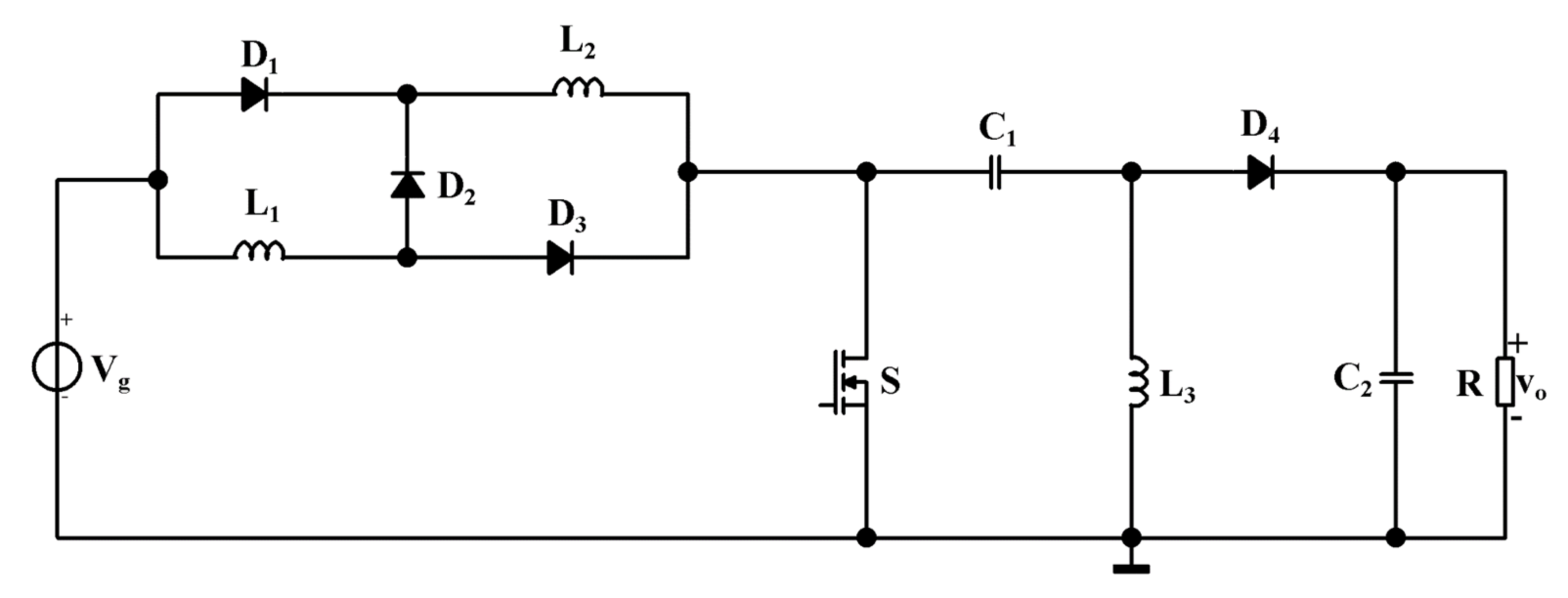
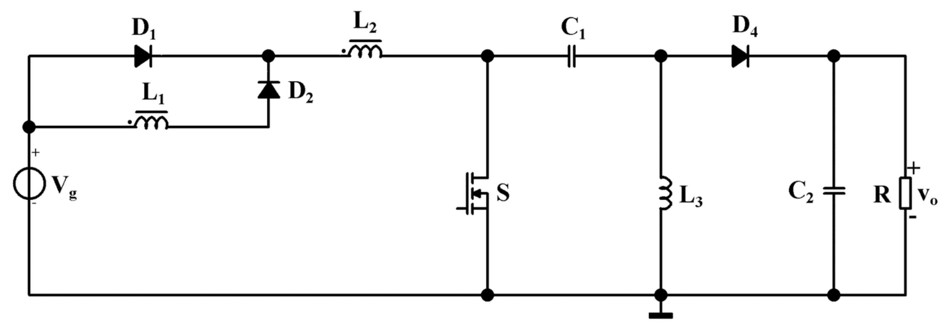
2. Steady State Analysis of the Proposed Hybrid SEPIC-Based Converter with Coupled Inductors

In [24], Prof. Ioinovici et al. proposed a new hybrid SEPIC converter with a switching Up 3 structure. The architecture of this topology was analyzed in [24,62] and is presented in Figure 1.
The idea of developing the novel converter proposed in this paper started by coupling the inductors L1 and L2. The authors also used this technique in other published research [63,64,65,66]. The coupling is assumed to be ideal and the numbers of turns corresponding to L1 and L2 are denoted as N1 and N2 respectively. The transformer ratio n defined as:
n = N 2 N 1
can be higher, lower, or equal to unity.
In this paper, the case when the transformer ratio is assumed to be lower than unity will be analyzed. It can be shown that, in this situation, diode D3 is always off and therefore it can be removed from the circuit. Taking this into account, the proposed topology is presented in Figure 2. It is obvious that it is simpler and cheaper than the previous one because one magnetic core and one diode are eliminated. The novel converter obtained consists of one active switch, three passive switches, an individual inductor, and a pair of coupled inductors, combined with one internal and one output capacitor.
In order to analyze the converter, all components are assumed to be ideal. Because the inductors are pefectly coupled, they will be modelled by an ideal transformer (IT) that has the transformer ratio n, together with a magnetizing inductor, LM, equal to L1. In Figure 3, the equivalent schematic is presented, and all the analyses will be developed on it considering the CCM operation. Noncapital letters will denote instantaneous variables, and capital letters will specify dc values or maximum values.
Considering the notations used in Figure 3, the ideal transformer equations are:
v 2 = n × v 1  
i 1 + n × i 2 = 0
The transistor is controlled by a pulse-width modulated (PWM) signal with a fixed frequency fs and a variable cycle D. The converter goes through two topological states, depicted in Figure 4a,b. In Figure 4a, in the first topological state, which lasts from 0 to DTs, both transistor S and diode D1 are on, while in Figure 4b, associated to the second topological state, which lasts from DTs to Ts, the diodes D2 and D4 are on.
The dc analysis is performed considering the small ripple assumption for the capacitor voltages and inductor currents. To calculate the dc voltages for the inner and output capacitors, the volt-second balance principle is invoked, and it can be written as in the following equations:
D × V g n + 1 D × V g V C 1 V C 2 1 + n = 0  
D × V C 1 + 1 D × V C 2 = 0
By solving Equations (4) and (5), the dc voltages across the internal capacitor, VC1, and across the output capacitor, VC2, are found as:
V C 1 = n + D n × V g  
V C 2 = D 1 D × n + D n × V g  
Because Vo = VC2, the ideal static conversion ratio can be obtained from (7):
M = D 1 D × n + D n  
The next step is to invoke the charge balance principle to calculate the dc magnetizing inductor current, ILM, and the dc output inductor current, IL3:
D × I L 3 + 1 D × I L M 1 + n   = 0
D × V C 2 R + 1 D × I L M 1 + n + I L 3 V C 2 R = 0
From (9) and (10), it follows that:
I L M = D 2 1 D 2 × n + D × 1 + n n × V g R  
I L 3 = D 1 D ×   n + D n × V g R  

3. Semiconductor Stresses and AC Analysis of the Proposed SEPIC-Based Converter

3.1. Semiconductor Stresses and Ripples Calculation

From the analysis carried out in the previous section, the semiconductor stresses are determined, neglecting the capacitor voltage ripples. These semiconductor stresses are also needed for the converter design.
The maximum voltage across switch S is obtained from the second topological state, while the dc transistor current stress can be found from the first topological state. The voltage across switch S is equal to the sum of the internal capacitor voltage, VC1, and the output capacitor voltage, VC2. By replacing VC1 and VC2 from (6) and (7), the transistor voltage stress is:
V S = n + D n × 1 D × V g  
The current flowing through the transistor is the sum between iLM/n and iL3. Hence, the dc transistor current stress is: D × I L M n + I L 3 . By replacing ILM and IL3 from (11) and (12), the transistor current stress is:
I S = D 2 × n + D 2 n 2 × 1 D 2 × V g R  
The voltage stress for diode D1 can be found from the second topological state being equal to V g V C 1 V C 2 1 + n . Using (6) and (7), it results that:
V D 1 = D n × 1 D × V g  
The current through diode D1 is equal to iLM/n, and therefore the dc current through D1 is D × I L M n . With ILM given by (11), one obtains:
I D 1 = D 3 × n + D × 1 + n n 2 × 1 D 2 × V g R  
Similarly, the voltage stress across diode D2 is obtained from the first topological state, while from the second topological state, the dc current through diode D2 results as:
V D 2 = V g n  
I D 2 = 1 D × I L M 1 + n = D 2 × n + D n × 1 D × V g R  
The voltage stress across D4 is the sum between VC1 and VC2. Using (6) and (7) it immediately follows that:
V D 4 = n + D n × 1 D × V g  
As D4 conducts the sum of the currents   i L M 1 + n + i L 3 in the second topological state, taking (11) and (12) into account, the dc D4 current is found as:
I D 4 = 1 D × I L M 1 + n + I L 3 = D × n + D n × 1 D × V g R  
Peak-to-peak inductor currents and capacitor voltages ripples are also invoked in the design equations and in the CCM operation conditions.
The magnetizing peak-to-peak current ripple can be written as:
Δ I L M = D × V g n × L M × f s  
The peak-to-peak current ripple for the inductor L3 is given by:
Δ I L 3 = D × n + D × V g n × L 3 × f s  
For the internal capacitor C1, the peak-to-peak voltage ripple is expressed as:
Δ V C 1 = D 2 × n + D n × 1 D × V g R × C 1 × f s  
The output capacitor peak-to-peak voltage ripple is:
Δ V C 2 = D 2 × n + D n × 1 D × V g R × C 2 × f s  
According to the CCM operation condition, it is necessary that the diodes be on during the whole topological state during which they are planned to conduct. This imposes the condition that the minimum diode current has to remain positive during the corresponding topological state. Taking into account that the converter includes three diodes, this will result in three CCM conditions. As the currents through D1 and D2 are equal to I L M n and I L M 1 + n respectively, for these diodes, the CCM condition is the same. In this case, the general condition will be:
I L M m i n = I L M 1 2 Δ I L M 0
By replacing ILM and ΔILM from (11) and (21), after some simple algebra the final condition is:
2 × L M × f s R 1 D 2 D × n + D × 1 + n  
The current flowing through D4 is i L M 1 + n + i L 3 , and iLM while iL3 have the same monotonicity. Therefore, the condition is I L M m i n 1 + n + I L 3 m i n > 0 , where I L M m i n = I L M 1 2 Δ I L M and I L 3 m i n = I L 3 1 2 Δ I L 3 . Replacing the ILM, IL3, ΔILM and ΔIL3 with their formulae from (11), (12), (21) and (22), the CCM condition for diode D4 becomes:
2 × L e × f s R 1 D 2 n + D  
where the equivalent inductor Le is:
L e = L M × n + D | | L 3 1 + n  

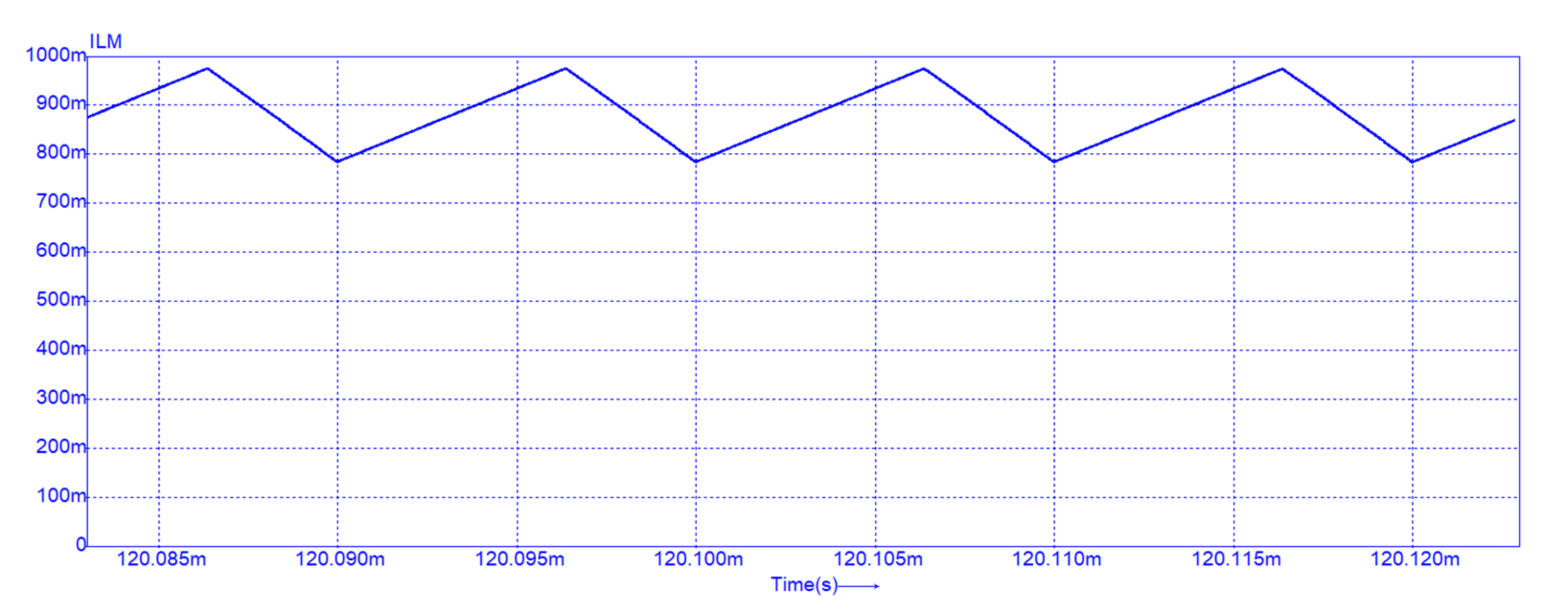
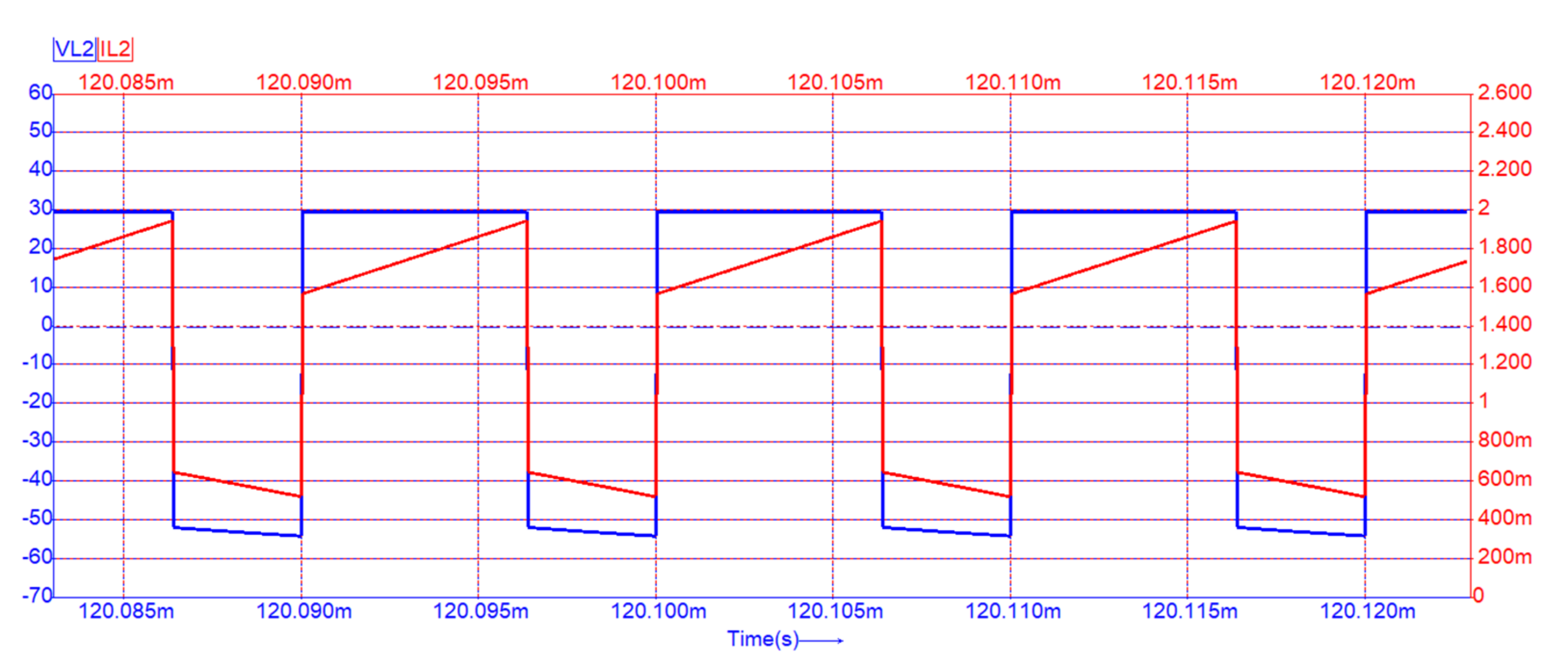
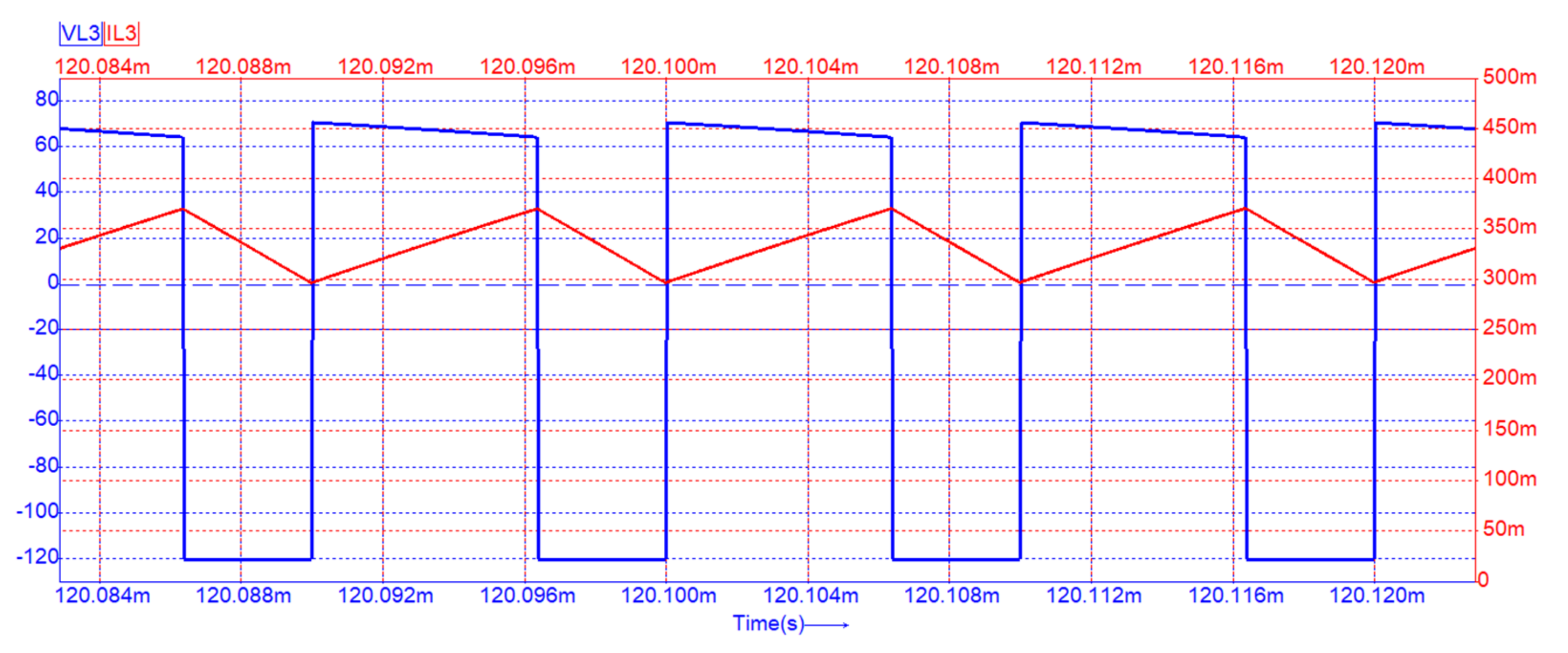
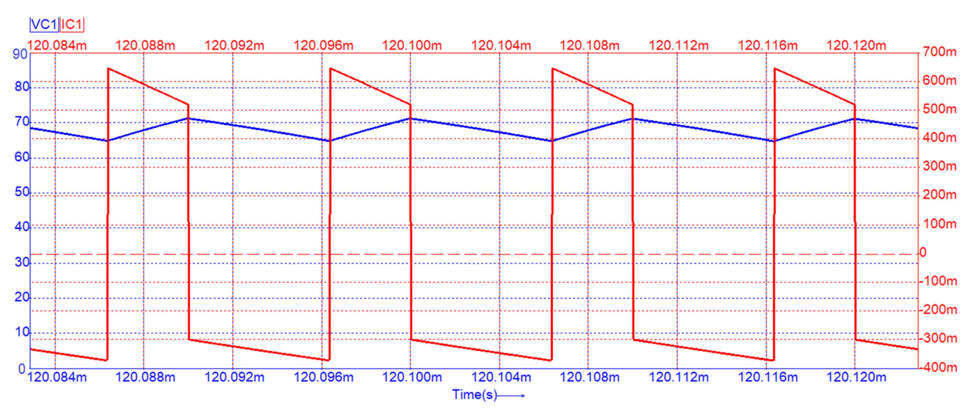
3.2. Steady State Theoretical Waveforms

The theoretical waveforms associated to the converter are presented in Figure 5 and Figure 6.
The magnetizing inductor voltage vLM is piecewise constant, exhibiting a rectangular shape, while the magnetizing inductor current iLM is piecewise linear, increasing until D∙Ts, because vLM is positive in the first topological state and decreasing in the second topological state, when the voltage is negative. Similarly, the same theoretical waveforms are associated for inductor voltage vL3 and inductor current iL3. Internal capacitor current iC1 and output capacitor current iC2 are piecewise constant, resulting in a piecewise linear internal capacitor voltage, vC1, and output capacitor voltage, vC2. The semiconductor waveforms, depicted in Figure 6, result from taking into account that, when “ON”, the semiconductor currents are linear combinations of inductor currents and the same is true for semiconductor voltages. These linear combinations values are also specified in Figure 6.

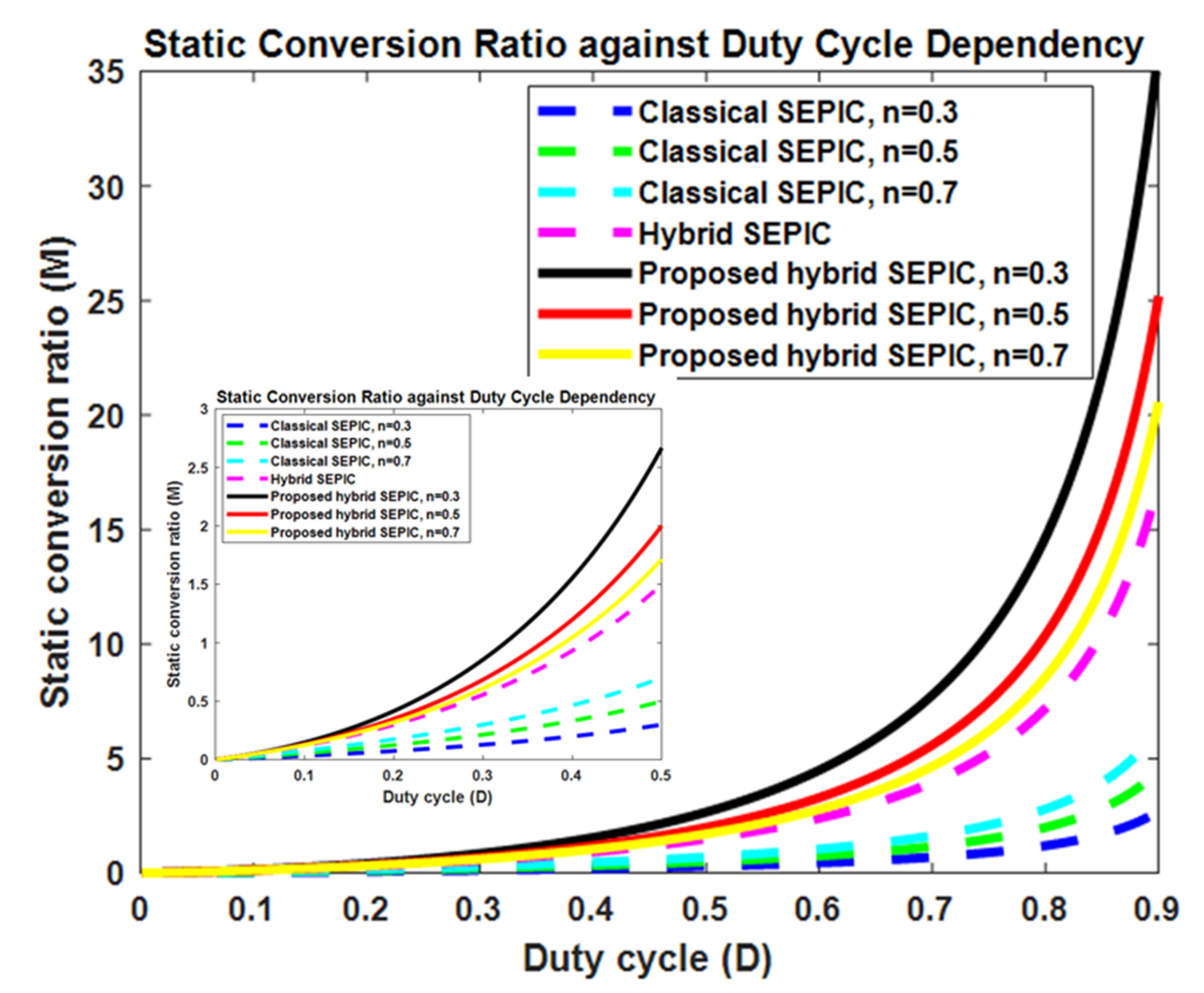
3.3. Comparative Study to Other Step-Down/Step-Up Topologies

Examining Equation (8), the duty cycle can be expressed in terms of the static conversion ratio and transformer ratio n as a solution of a second-degree equation:
D = n × 1 + M × n 2 × 1 + M 2 + 4 × n × M 2
The dependency of the static conversion ratio against the duty cycle for the classical isolated SEPIC [61], the hybrid SEPIC from [24] and the proposed hybrid SEPIC-based converter is presented in Figure 7. For a better representation, a detail for a duty cycle between [0–0.5] is provided.
At a first glance, the step-down and step-up allure of the proposed converter can be observed. From (29) and Figure 7, it can be observed that the proposed SEPIC converter starts to step up at a lower duty cycle value, compared to the isolated and hybrid SEPIC, or, in other words, at the same turns ratio, a higher static conversion ratio is achieved for the proposed converter at the same duty cycle, compared to the same converters. Figure 7 also reveals the fact that the lower the value of n, the more step-up is achieved, thus recommending the converter for step-up applications where a big difference between the input and output voltage is needed.
Another comparison, where the comparative parameters are the number of active and passive semiconductors, the number of cores/windings, the total number of components, the system order, the expression of the static conversion ratio M, the expression of the duty cycle D, and the current and voltage semiconductor stresses, is realized in Table 1. The comparison is made between the classical Buck-Boost, classical non-isolated SEPIC, hybrid SEPIC and proposed hybrid SEPIC converter. For a fair comparison, the converters are supposed to be supplied by the same input voltage Vg, and to deliver the same output voltage Vo on the same load R. Consequently, the conversion ratio M and the output power Po are the same.
Analyzing the results from Table 1, it can be remarked that each topology has only one transistor. The proposed SEPIC-based converter has two additional diodes, in comparison to the classical Buck-Boost or SEPIC converter, and one diode less if it is compared to the hybrid SEPIC from [24]. The lowest system order is the classical Buck-Boost, followed by the classical SEPIC and the proposed SEPIC. From Table 1, it can be seen that the static conversion ratio for the proposed SEPIC topology is (1 + D/n) times higher than the classical SEPIC, or Buck-Boost converter. Therefore, in the step-up region, a wide static conversion ratio is achieved at a moderate duty cycle, and this can be observed also from the dependency of the static conversion ratios against the duty cycle for the proposed converter, for the classical and the hybrid SEPIC converters presented in Figure 7.

4. Design Example for the Proposed Converter

In the design example, the converter is used in a PV system and, therefore, the requirements for the proposed SEPIC-based converter depend on the PV panel characteristics. Two PV modules MWG-20 will be used for the experiments. The PV modules will be connected in series, in order to increase the input voltage. In standard test conditions (STC) for a solar irradiance G = 1000 W/m2 and temperature T = 25 °C, one PV module has the following parameters:
  • Peak power: Pmax = 20 W
  • Maximum power point current: Imp = 1.14 A
  • Maximum power point voltage: Vmp = 17.49 V
  • Short circuit current: Isc = 1.22 A
  • Open circuit voltage: Voc = 21.67 V
  • The converter was designed according to the following parameters:
  • Input voltage range was between: Vg = 30 ÷ 35 V − correlated to Vmp
  • Maximum output power: Po = 40 W
  • Switching frequency: fs = 100 kHz
  • Output voltage: Vo = 120 V
  • Output voltage peak-to-peak ripple: ΔVC2 = 300 mV
  • Transformer ratio: n = 0.5
The minimum and maximum static conversion ratios are obtained from Equation (8):
M m i n = V o V g m a x = 3.42
M m a x = V o V g m i n = 4
The necessary duty cycle range can be calculated using (29) and will result in D     [0.6070, 0.6375].
The value for the load resistor is given by:
R = V o 2 P o = 360   Ω
Imposing the peak-to-peak magnetizing inductor current ripple given by (21) not to exceed 25% of the dc magnetizing inductor current value (11), the magnetizing inductor can be calculated. The condition will be:
Δ I L M   1 4 × I L M
From Equations (33), (21) and (11) the minimum magnetizing inductor formula can be found:
L M 4 × 1 D 2 × R D × n + D × 1 + n × f s  
In a similar way, the condition for L3 inductor current will look like:
Δ I L 3   1 4 × I L 3
and from (35), (22), and (12) the minimum inductor L3 value can be found as follows:
L 3 4 × 1 D × R f s
The equations for the inner and output capacitors are designed imposing that the voltage ripple across the inner capacitor be less than ten percent of its dc value and for the output capacitor to ensure an output voltage ripple less than the value imposed by the specifications.
Using (6) and (23) the minimum required value for the internal capacitor, and from (7) and (24) the minimum required value for the output capacitor can be calculated:
C 1 10 × D 2 1 D × R × f s  
C 2 D 2 × n + D × V g n × 1 D × R f s × Δ V C 2
The minimum value of the magnetizing inductor LM calculated with Equation (35) will be equal to the value of inductor L1, LM = L1 = 1.7 mH. The value for L2 is determined using L2 = n2∙LM, so L2 = 425 µH. The minimum inductor value L3, calculated from (36) is L3min = 5200 µH. The minimum value of the inner capacitor was obtained from (37) and that for the output capacitor from (38), and they are C1min = 0.26 µF and C2min = 6.72 µF. The inductors were manufactured in the laboratory with the following values: L1 = 2 mH, L2 = 503 µH and L3 = 5900 µH. Taking into account the practical values obtained in the laboratory for L1 and L2, the transformer ratio n resulted as n = 0.5014. For the capacitors, the following standard values were chosen: C1 = 0.33 µF and C2 = 10 µF.
The transistor voltage stress can be calculated from (13), and it is VS = 197 V. According to (14), its average current will be IS = 1.33 A. The voltage and current stresses associated to diode D1 can be calculated from (15) and (16), respectively, resulting in: VD1 = 108 V and ID1 = 1.12 A. The smallest voltage and current stresses are related to the diode D2: VD2 = 70 V and ID2 = 0.21 A, calculated from (17) and (18). The value of the voltage stress on diode D4 is equal to the voltage stress of the transistor, VD4 = 197 V. From (20) diode D4 current stress is ID4 = 0.33 A.

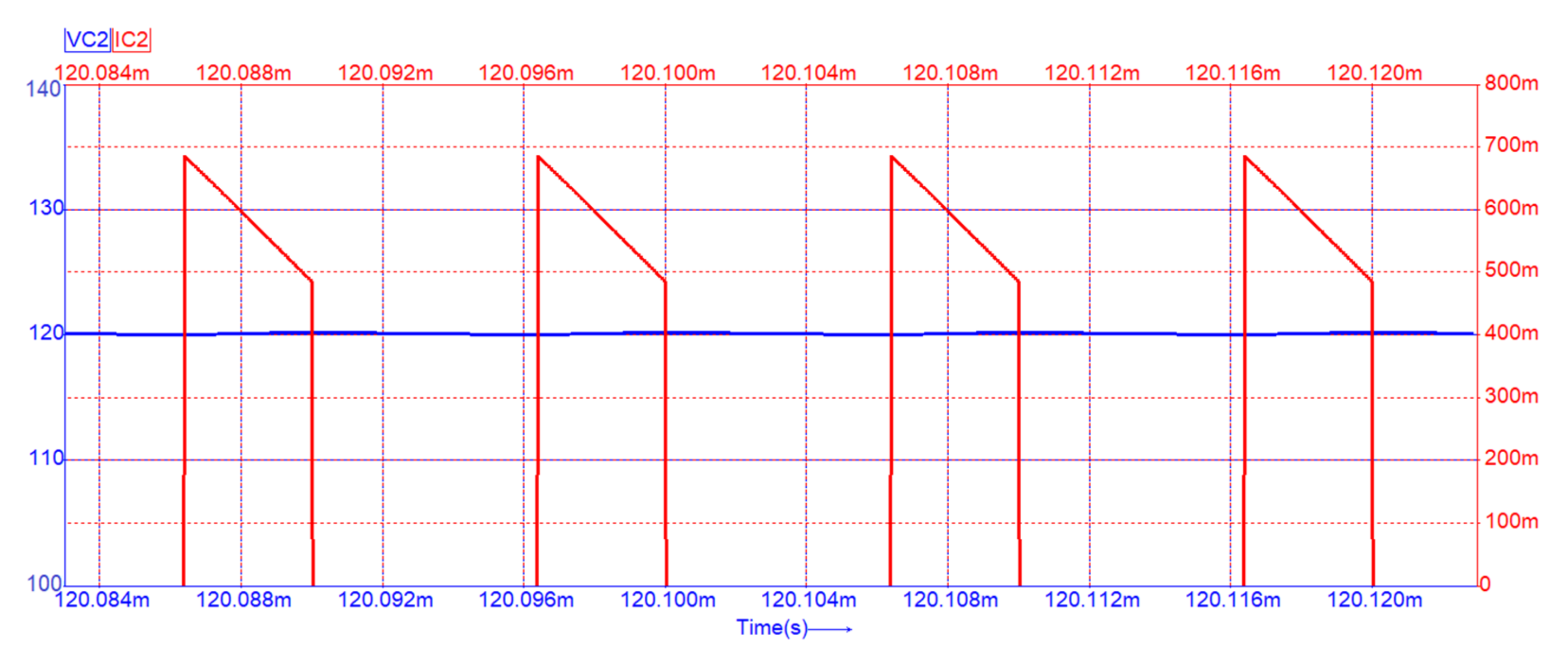
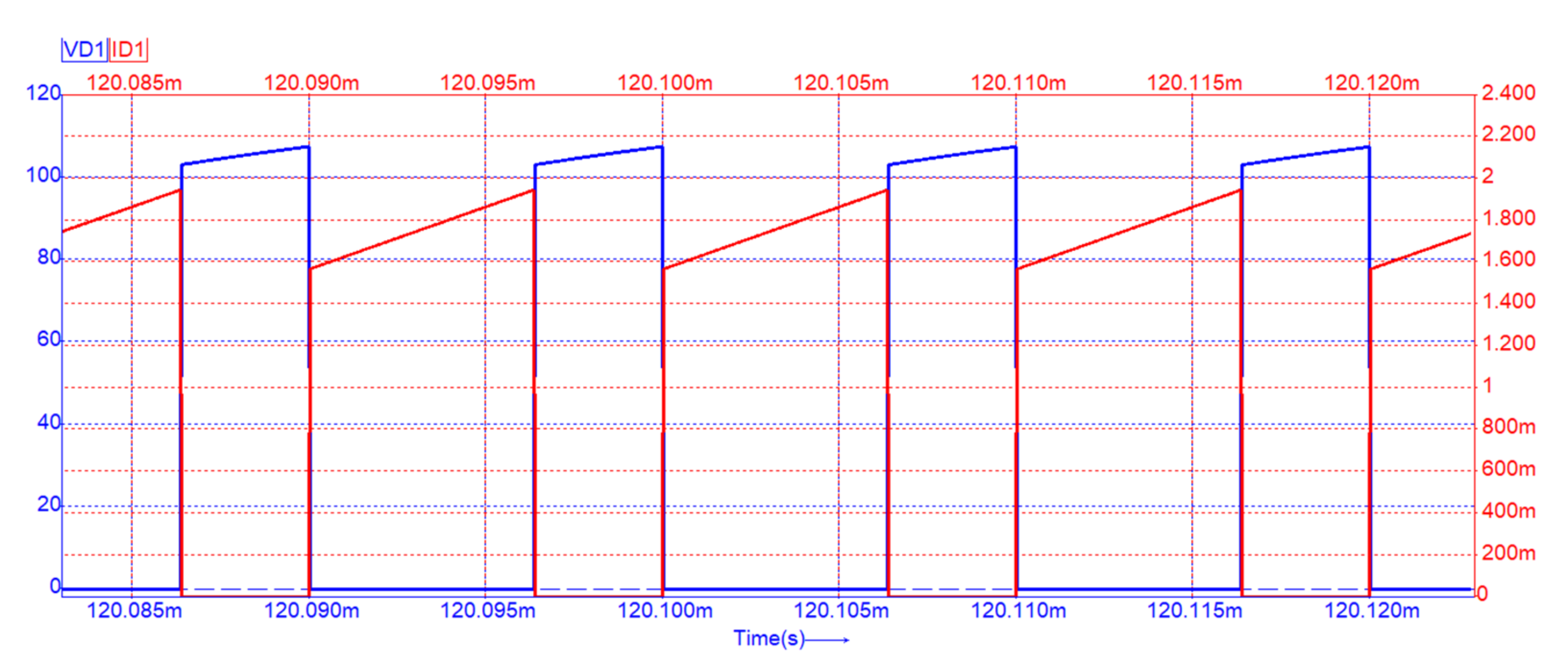
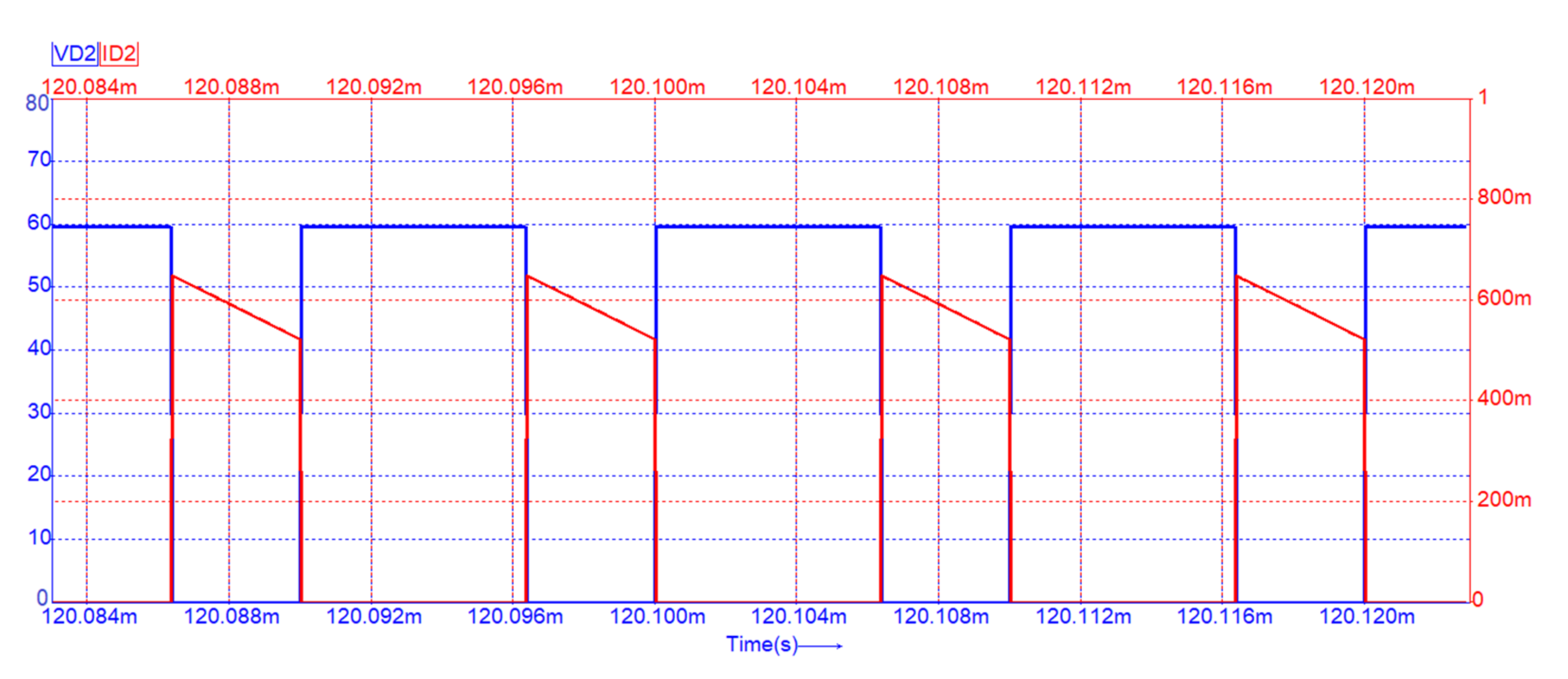
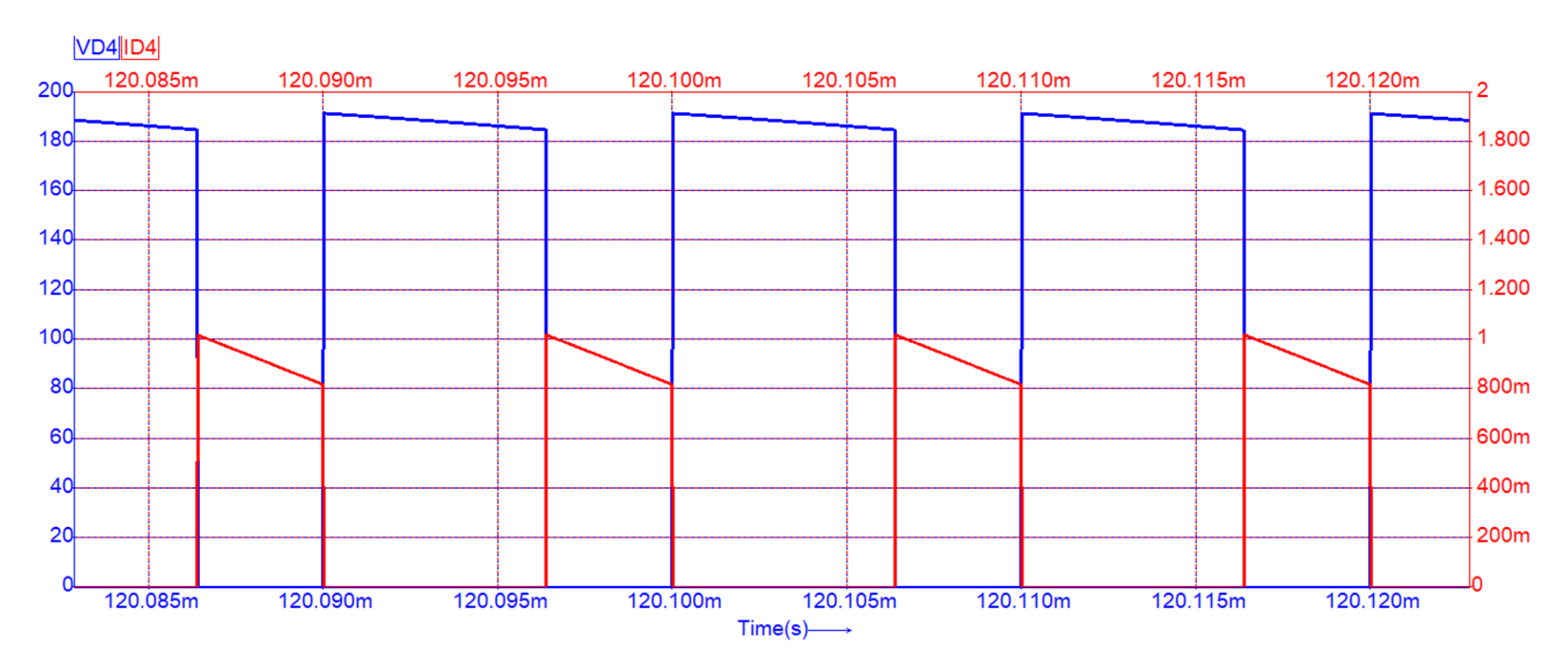
5. Simulations and Experimental Results

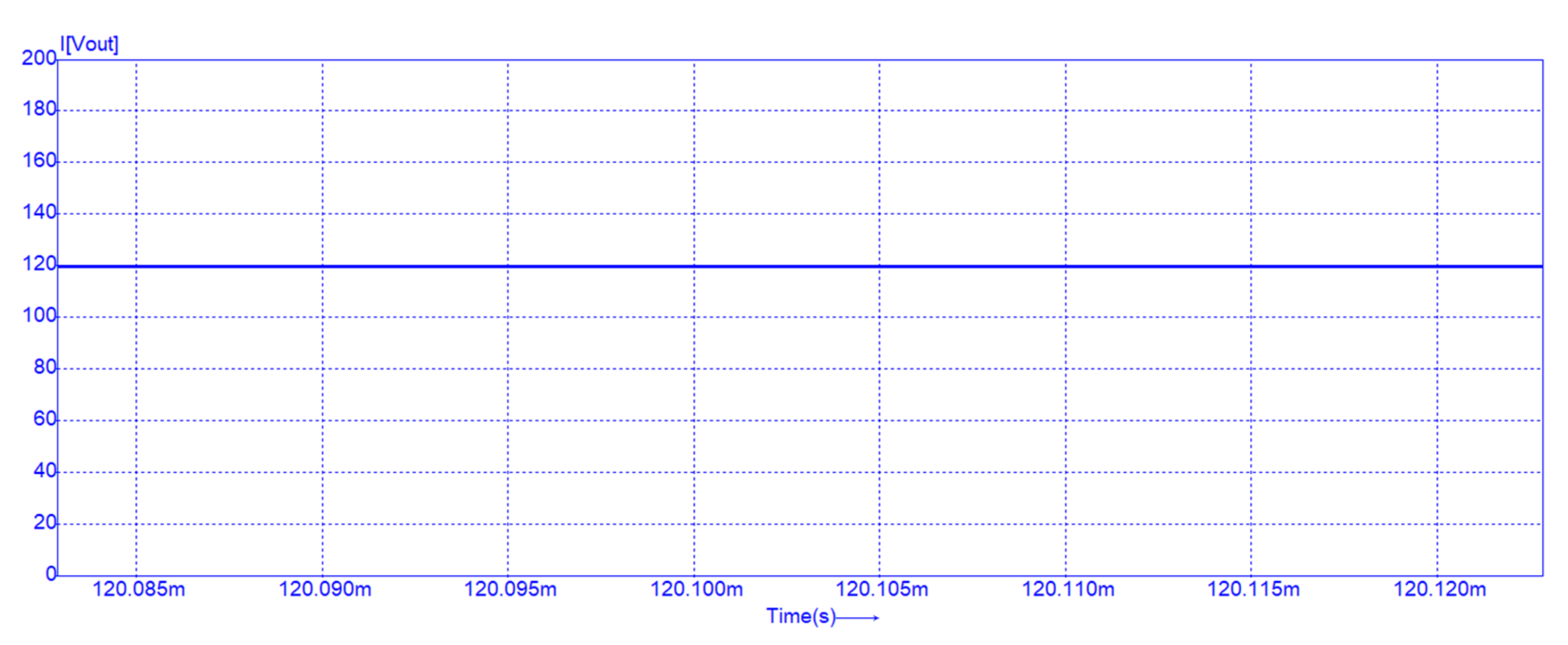
5.1. Simulation Results

A simulation of the ideal SEPIC-based dc-dc converter with coupled inductors was performed using Caspoc software [67]. This simulation was realized as a first validation of the theoretical considerations. The values of the components are the same as those from the design example. The simulation is made in an operating point, considering the input voltage Vg = 30 V, the static conversion M = 4. For these values, the duty cycle is D = 0.6375.
The dc output voltage, Vo, predicted by the simulation was 120 V, as Figure 8 reveals, exactly as theoretically calculated with (7). In Figure 9, the magnetizing inductor current is presented, confirming its triangular shape, obtained in Caspoc with the help of the mathematical blocks. For inductor L1, the first part of the triangular shape of the magnetizing current can be seen in Figure 10. The second part of the triangular shape of the magnetizing current can be seen in Figure 11, as the inductor L2 current. The voltage and current for inductor L3 are presented in Figure 12. The correct CCM operation of the converter is proven by the voltages and currents for the coupled inductors L1 and L2, and inductor L3. The voltage and current for the inner capacitor are presented in Figure 13 and, for the output capacitor, are depicted in Figure 14. In Figure 15, Figure 16, Figure 17 and Figure 18, the voltage and current for the transistor and diodes are presented.
The simulation results completely validated the theoretical considerations, both qualitatively and quantitatively.

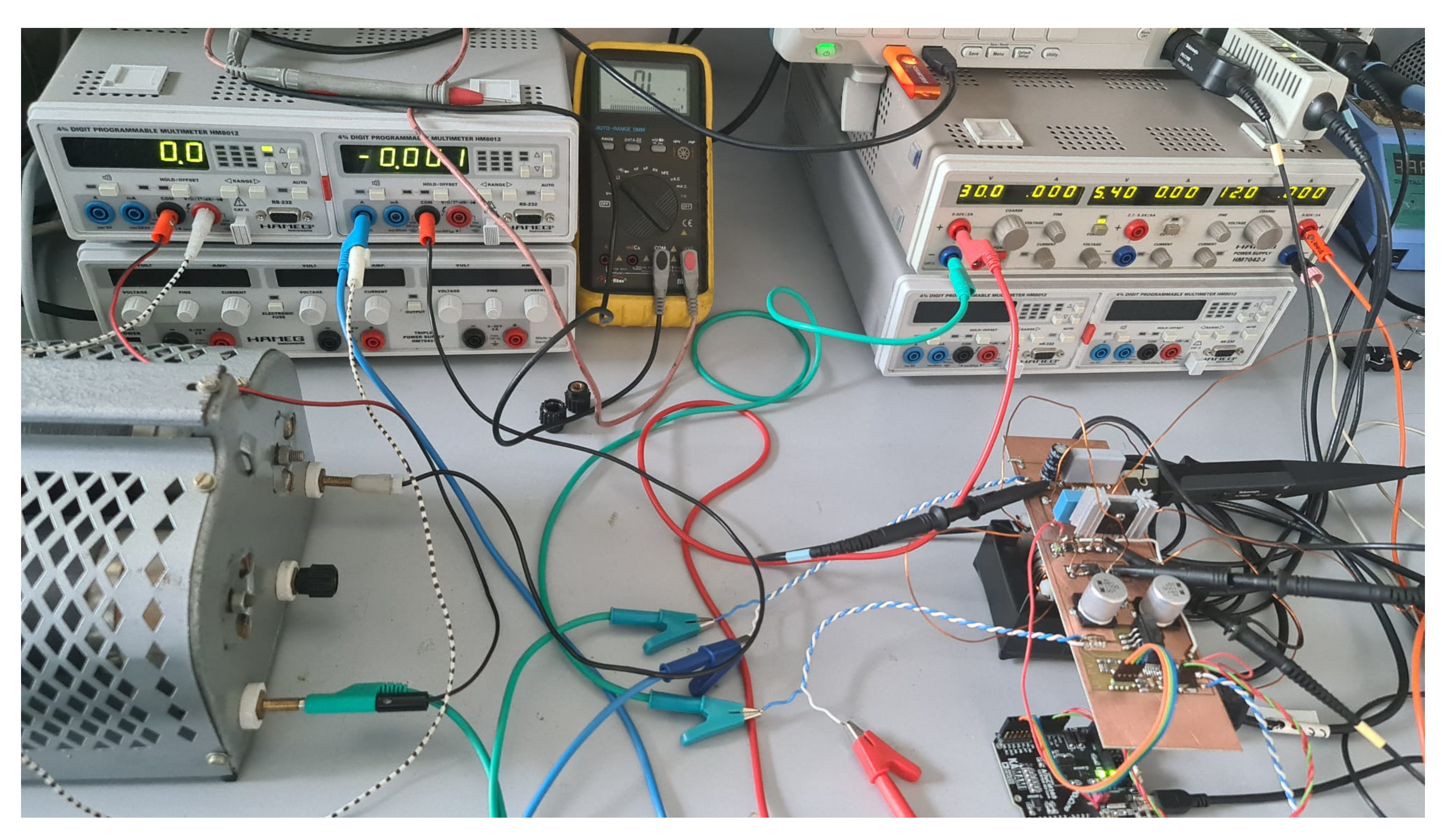
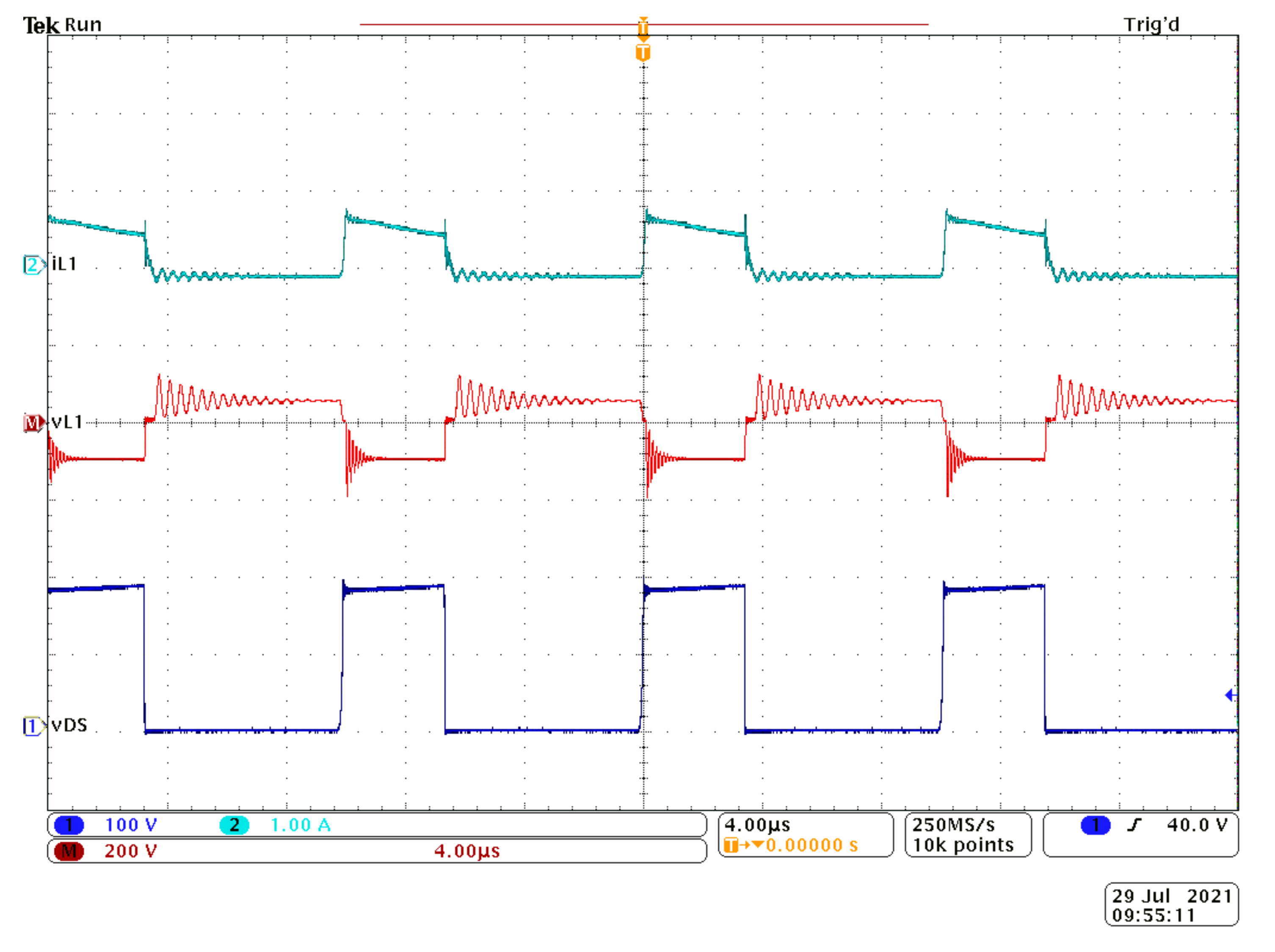
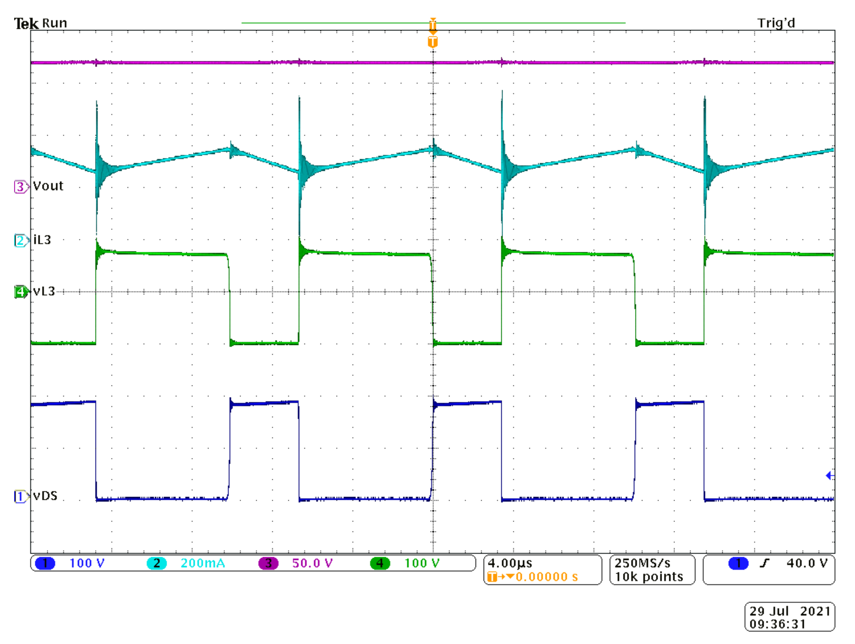
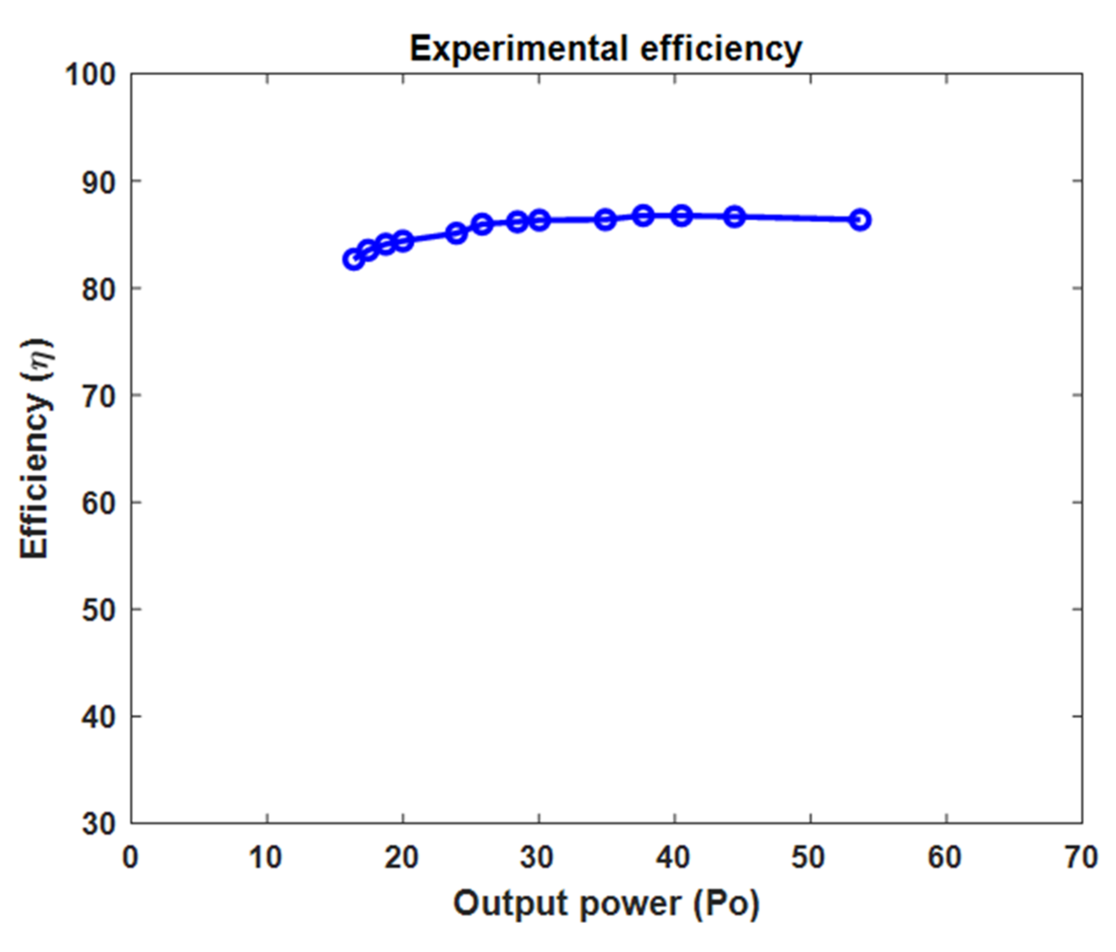
5.2. Experimental Results

A prototype of the proposed SEPIC converter was built in order to prove its functionality. The design parameters were the same as the ones in the design example and simulation. The semiconductors used were: S = STMicroelectronics STW70N60M2 and diodes D1,2,4 = Silicon Carbide Diodes from STMicroelectronics STPSC4H065-type. The coupled inductors L1 and L2 were built on the same E71/33/32-3C94 FERROXCUBE core, and the turns numbers were manually adjusted in order to obtain the desired inductor values. For inductor L3, a separated core of the same type was used. The experimental waveforms were obtained with a fixed input voltage of Vg = 30 V, a fixed switching frequency of fs = 100 kHz and a load of R = 360 Ω. In Figure 19, the proposed SEPIC converter, together with the equipment used, can be observed.
The reference signal that is present in all waveforms on the oscilloscope is the drain-to-source transistor voltage. In Figure 20, the second waveform is the voltage across inductor L1 (in red) and the third waveform is the inductor L1 current (shown in cyan). In Figure 21, the first waveform is the drain-to-source voltage, (blue), the second one is the voltage across winding L2 (red), followed by the current through inductor L2 (cyan), with the last waveform being the output voltage (purple). The waveforms for inductor L3 are presented in Figure 22. After the reference signal in blue, the voltage across inductor L3 (in green) and the current through inductor L3 (light blue) can be observed, while the last waveform is the output voltage (purple). It is confirmed that the acquired waveforms are in good accordance to those from the simulation.
In Figure 23, the dependency of the efficiency against the output power at a constant output voltage of 120 V is presented.

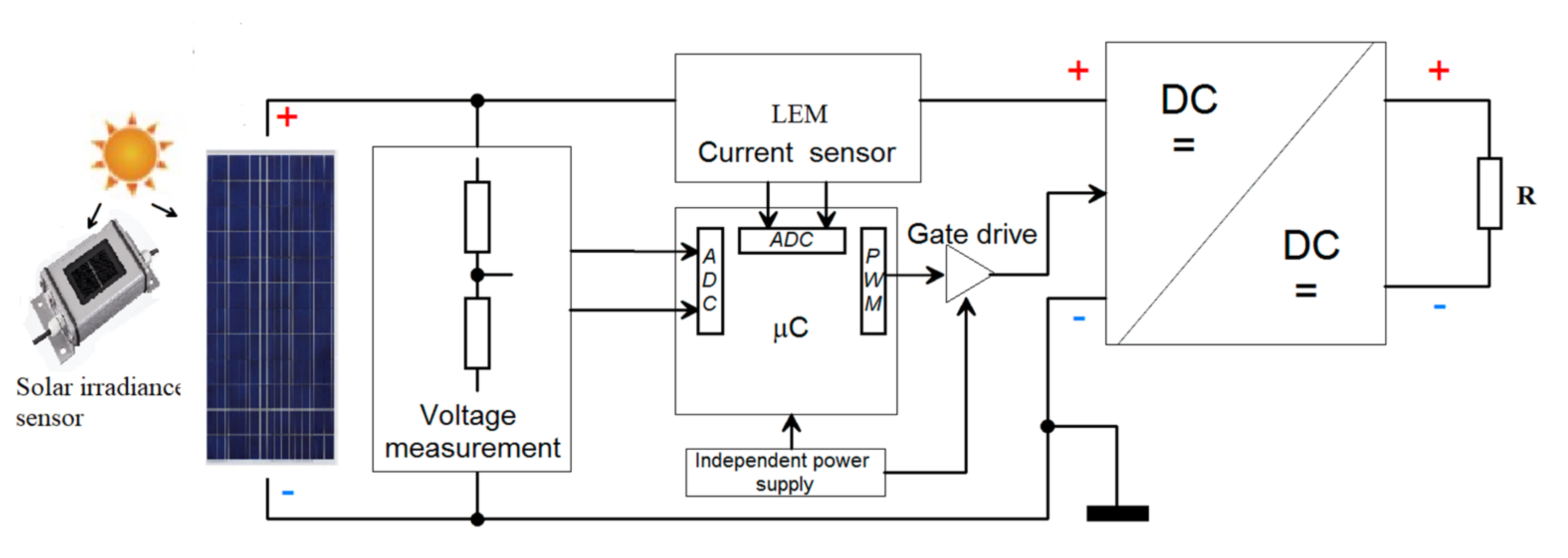
6. Applicability of the Proposed SEPIC Converter in a PV System

For proving the ussefulnes of the proposed SEPIC-based converter in a PV application, a PV system with the block diagram presented in Figure 24, was built.
The structure of the PV application is similar with the block diagram presented in [64]. The chosen maximum power point (MPP) algorithm was perturb and observe (P&O), and it was implemented in an ADuCino development board equipped with the ADuCM360 ARM microcontroller (Analog Devices, Greater Boston, MA, USA) [68]. The current transducer used in this application was LEM HO-8-NSM/SP33 [69]. A resistive divider was used to measure the voltage across the PV modules. The MPPT algorithm is described in detail in the authors’ work [64].

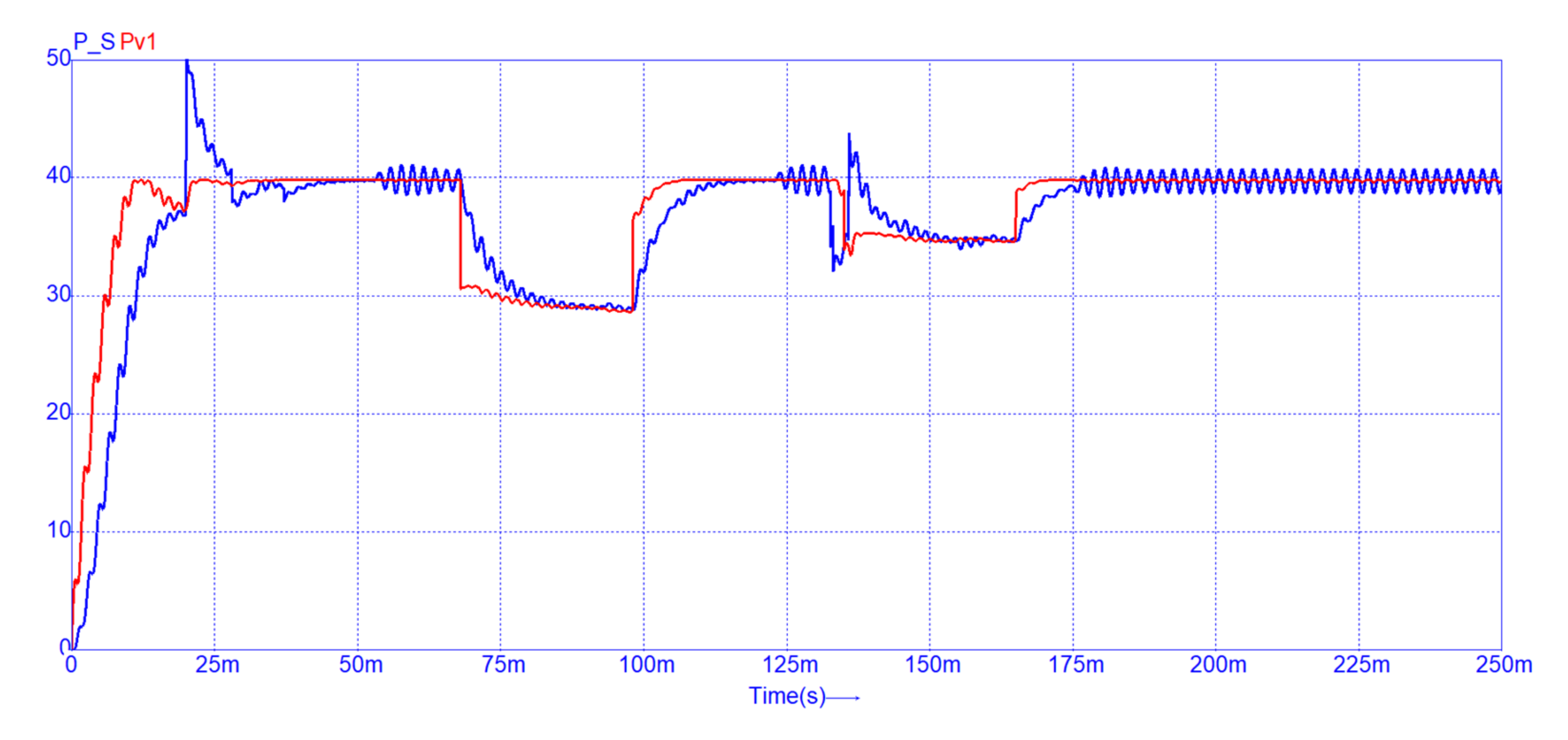
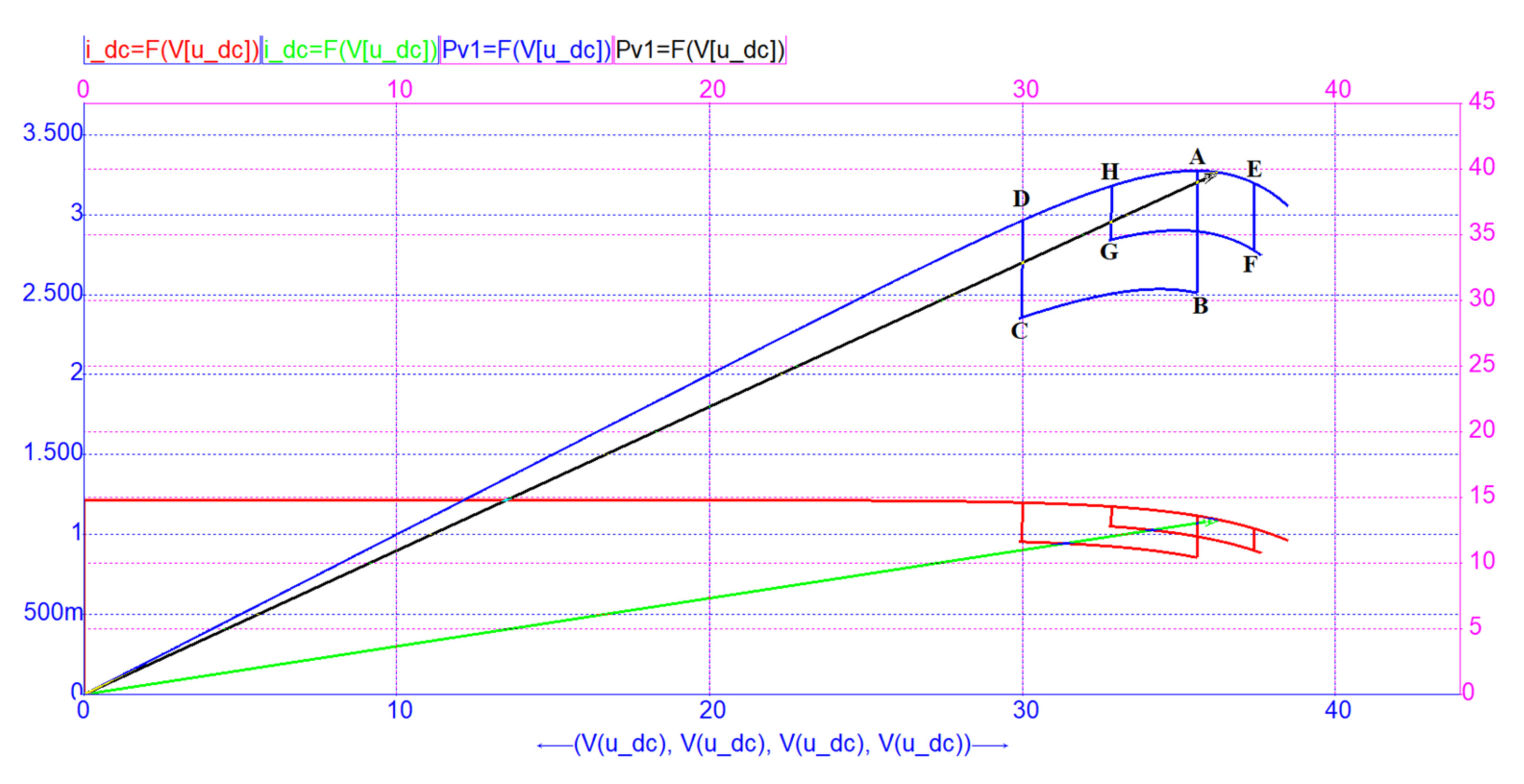
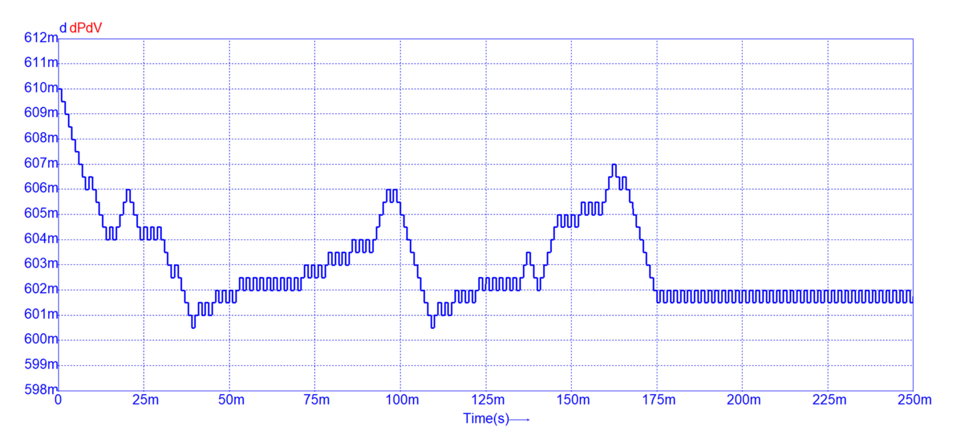
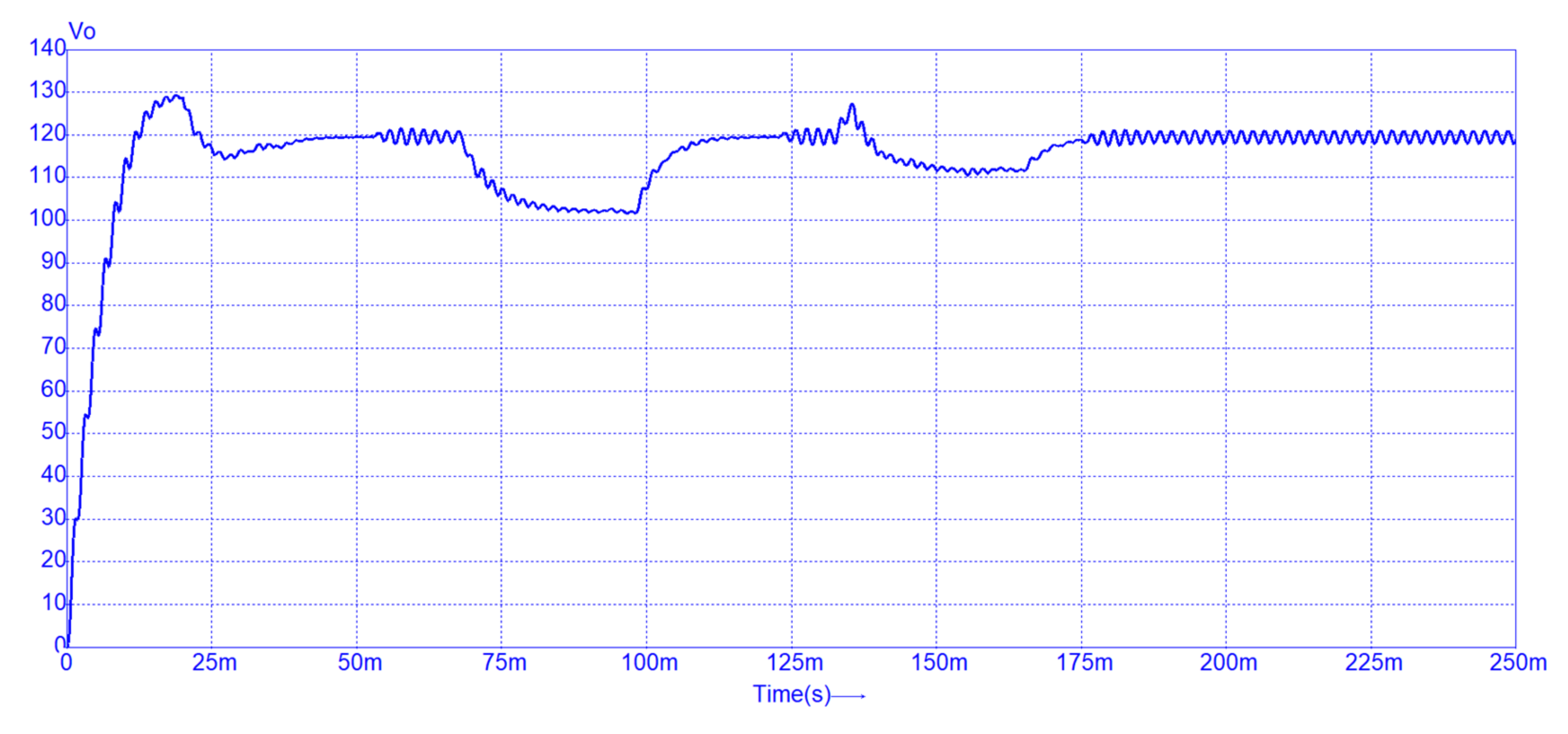
6.1. Simulation Results of the PV System Using the Proposed SEPIC Converter

To prove the utility of the proposed SEPIC-based converter in the PV system, a simulation that follows the scenario below was performe. All the changes encountered were step changes.
-
at start-up T1 = 0 ms, the irradiance was set to G1 = 1000 W/m2, and the load resistance was R = 450 Ω;
-
at T2 = 20 ms, the load resistance suffered a change to R = 325 Ω;
-
at T3 = 28 ms, the load resistance was changed to R = 350 Ω;
-
at T4 = 37 ms, the load resistance was modified to R = 360 Ω;
-
at T5 = 68 ms, the irradiance was suddenly modified from G1 = 1000 W/m2 to G2 = 800 W/m2;
-
at T6 = 98 ms, the irradiance was set back to G3 = 1000 W/m2;
-
at T7 = 133 ms, the output resistance was changed to R = 460 Ω;
-
at T8 = 135 ms, the irradiance was set from G3 = 1000 W/m2 to G4 = 900 W/m2;
-
at T9 = 136 ms, the output resistance was changed back R = 360 Ω;
-
the last change was at T10 = 165 ms, when the irradiance was modified from G4 = 900 W/m2 to G5 = 1000 W/m2.
The simulation time was 250 ms. The simulation step chosen was 20 ns, and the results were displayed each one hundred simulation steps. In Figure 25, the input (red) and the output (blue) power against time are represented. With these characteristics, the changings according to the scenario can be easily identified, and it can be remarked that the MPPT control regulates the absorbed power from the panel. The regulated power value is about 40 W at an irradiance equal to 1000 W/m2, 30 W at 800 W/m2 and around 35 W at a solar irradiance of 900 W/m2.
The current-voltage and power-voltage characteristics of the PV module can be seen in Figure 26. During the simulation, the instantaneous position of the operating point (OP) on the current-voltage (I-V) characteristic is shown with the green arrow, while the black arrow points to the instantaneous position of the operating point on the power-voltage (P-V) characteristic. The system is able to reach the MPP, even if the OP is located before or after the MPP. The MPP can be found at the point marked on the graph with “A”. Because the load was initially set to R = 450 Ω, the characteristics passed through the MPP, and overpassed point “E”. Changing the value of the load to R = 325 Ω determined the return to point “A”, but overpassed point “A” to the left. Adjusting the resistor to R = 350 Ω caused the return to point “A” but slightly exceeded to the right, with small oscillations around point “A”. When T4 = 37 ms, the output resistance was changed to R = 360 Ω, which determined the return to and placement in point “A,” corresponding to the MPP. A step transition in solar irradiance from G1 = 1000 W/m2 to G2 = 800 W/m2 produced a displacement from points “A” to “B” and an evolution on the PV characteristic related to point “C”. A step increase in the irradiance to 1000 W/m2 produced a jump of the characteristics from “C” to “D” and a progression of the PV characteristic that ended with the value of the solar irradiance corresponding to point “A”. Changing the value of the load to R = 460 Ω determined the exceedance of point “A” to the right. Because at T8 = 135 ms, the irradiance was set from G3 = 1000 W/m2 to G4 = 900 W/m2, again a jump took place from point “E” to point “F” and a search of the MPP on the characteristic corresponding to 900 W/m2. When the load was changed back to R = 360 Ω, it determined a return to the left of the characteristics, finally reaching the point “G”. The last modification of the solar irradiance, back to G5 = 1000 W/m2 produced a jump from “G” to “H” and a displacement on the solar irradiance characteristic to the point “A”. At the end, small oscillations around point “A” could be observed due to the P&O MPP algorithm.
The duty cycle evolution that results from the P&O algorithm is depicted in Figure 27. At the end, when the irradiance and the load do not modify anymore, the duty cycle is slightly modified around the expected value of 60%.
Figure 28 presents how the output voltage modifies along the proposed scenario. It is confirmed that the desired dc output voltage value of 120 V can be achieved if the irradiance and the load are high enough and they do not modify.
An overall examination of Figure 25, Figure 26, Figure 27 and Figure 28, clearly reveals the correlations between the input and output power characteristics, current-voltage and power-voltage characteristics, duty cycle and output voltage evolution regarding the time moments when changes occur.

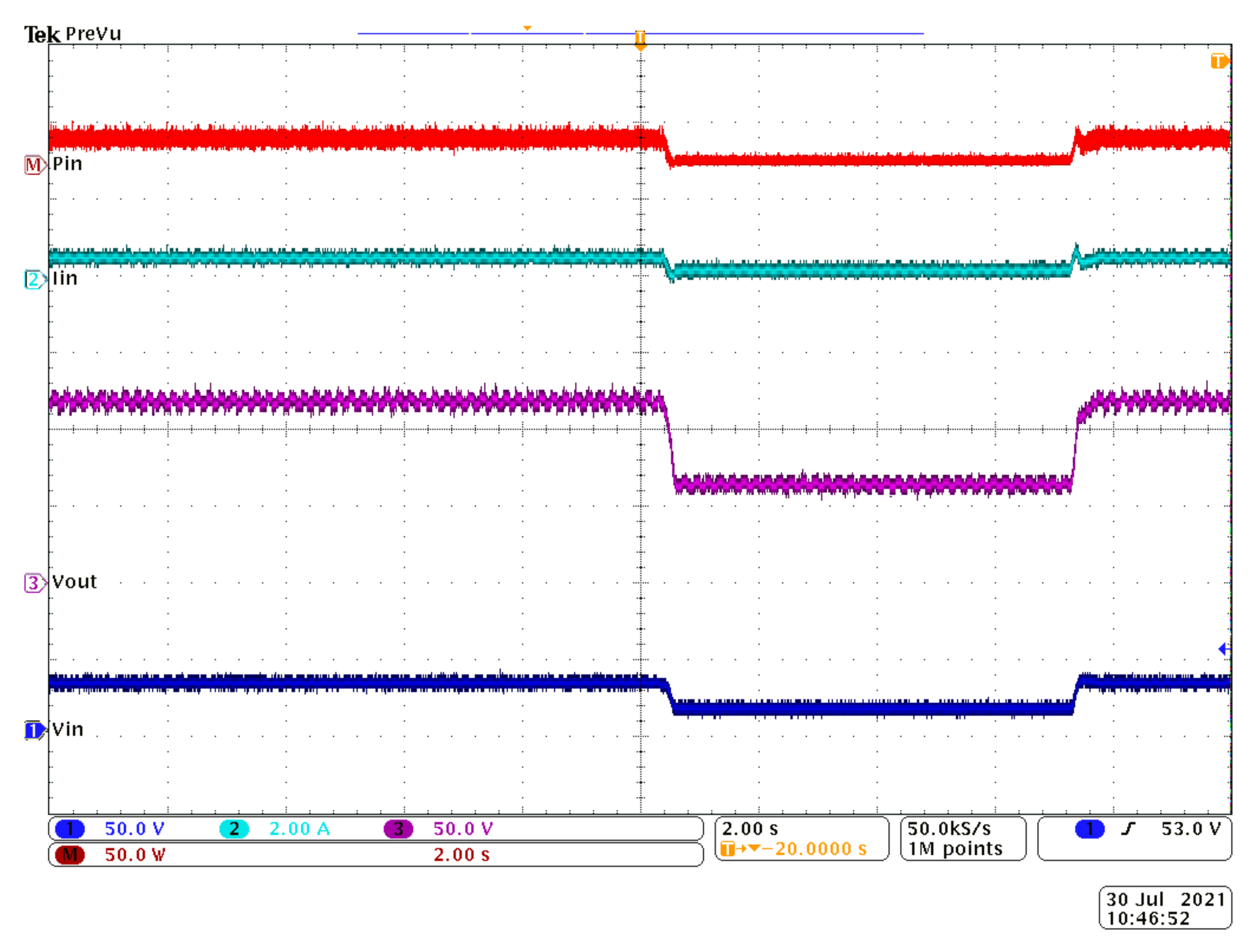
6.2. Experimental Results of the PV System Using the Proposed SEPIC-Based Converter

In this section, the novel proposed converter supplied by two PV panels connected in series and having P&O as a MPPT method is presented. For solar irradiance and PV temperature measurement, a pyranometer [70] was used. The pyranometer produces a voltage (VGPV) proportional to the incident solar irradiance. For the PV temperature measurement (TPV), the other pyranometer voltage (VTPV) is measured and the temperature can be found according to the formula [70]:
T P V = V T P V 1.84 0.092   ° C
In Figure 29 and Figure 30, for an irradiance of 885.6 W/m2 the corresponding VGPV = 7.38 V and VTPV = 8.24 V. According to (39), the PV temperature is equal to TPV = 69.56 °C. In Figure 29, the oscilloscope capture shows the start-up, which lasts approximately 5 s.
In the down to up order, the first waveform drawn in dark-blue and labeled “Vin” is the input voltage. In the beginning, it is equal to the open-circuit voltage of the PV panels, of about 42 V, and then it decreases according to the characteristic to about 35 V. The MPP is reached after approximately 5 s, and this can be seen on the third waveform labeled “Vout” (in purple). The P&O algorithm continuously modifies the duty cycle by increasing and decreasing it with one step. Because the irradiance is constant, the converter is maintained around the same OP. The output voltage in this case is equal to 110 V. The second signal is the input current, labeled “Iin” and depicted with cyan. The fourth waveform presented, labeled “Pin”, is the instantaneous power at the input provided by the PV cell. This power is displayed on the oscilloscope, computing the product between the voltage and current at the input. To demonstrate the functionality of the P&O control algorithm, the input power needs to be maximized. As the current increases and the input voltage slightly decreases, the input power provided by solar conversion increases and proves the correct behavior of the control algorithm. In Figure 30, the same waveforms are shown in different order: “Vin”, “Vout”, “Iin” and “Pin” for the following scenario. Because the measurements were performed on a sunny day, without any cloud in the sky, in order to prove the functionality of the converter driven by the P&O algorithm, after about 10.4 s, a part of the PV panel was shaded for approximately 6 s. The input voltage and power decrease can be observed in Figure 30, and the steps of the P&O implementation are also visible, validating the effectiveness of the P&O implementation.

7. Discussion

A new step-up/step-down converter with a step-up characteristic steeper than that of the classical SEPIC and hybrid SEPIC is introduced. As a result, the new topology is suitable in applications where an output voltage much higher than the input voltage is needed. Inductor coupling introduces an additional degree of freedom, and this allows for the minimization of certain stress values. After deriving the steady state equations and sketching the main waveforms, design equations were provided, and the simulations validated the theoretical concepts. In order to prove the feasibility and usefulness of the proposed converter, a PV solar system was built around it. It is shown that, using the P&O algorithm, the system can be maintained on the MPP and the maximum power capabilities of the PV panel can be used. In addition to its higher step-up capability, the converter has the advantage of offering a non-inverting output voltage and a non-floating transistor, which simplifies the control.

Author Contributions

All authors contributed to this research. Conceptualization and study design I.-M.P.-C. and D.L. Formal analysis, I.-M.P.-C. and D.L. MATLAB program development, I.-M.P.-C. and D.L. Performed the Caspoc simulations for the new proposed SEPIC-based converter, I.-M.P.-C. Performed the Caspoc simulations for the MPPT algorithm, S.P. Software algorithm, S.P. and D.L. Experiments, I.-M.P.-C., D.L. and S.P. Validation, I.-M.P.-C., D.L. and S.P. Writing original draft, I.-M.P.-C. Writing-review and editing, D.L., I.-M.P.-C. and S.P. All authors have read and agreed to the published version of the manuscript.

Funding

This work was supported by a grant of the Ministry of Research, Innovation and Digitization, CNCS/CCCDI—UEFISCDI, project number PD76/2020, within PNCDI III.

Conflicts of Interest

The authors declare no conflict of interest.

References

  1. IRENA. Global Energy Transformation: A Roadmap to 2050; International Renewable Energy Agency: Abu Dhabi, United Arab Emirates, 2018. [Google Scholar]
  2. IEA. Net Zero by 2050. A Roadmap for the Global Energy Sector IEA; IEA: Paris, France, 2021; Available online: https://www.iea.org/reports/net-zero-by-2050 (accessed on 1 October 2021).
  3. WWF—World Wide Fund for Nature (Formerly World Wildlife Fund). 100% Renewable Energy Report; WWF: Gland, Switzerland, 2011; Available online: http://awsassets.panda.org/downloads/the_energy_report_lowres_111110.pdf (accessed on 1 October 2021).
  4. Koç, Y.; Birbir, Y.; Bodur, H. Non-isolated high step-up DC/DC converters—An overview. Alex. Eng. J. 2021, 61, 1091–1132. [Google Scholar] [CrossRef]
  5. Raghavendra, K.V.G.; Zeb, K.; Muthusamy, A.; Krishna, T.N.V.; Prabhudeva Kumar, S.V.S.V.; Kim, D.-H.; Kim, M.-S.; Cho, H.-G.; Kim, H.-J. A Comprehensive Review of DC–DC Converter Topologies and Modulation Strategies with Recent Advances in Solar Photovoltaic Systems. Electronics 2020, 9, 31. [Google Scholar] [CrossRef] [Green Version]
  6. Affam, A.; Buswig, Y.M.; Othman, A.-K.B.H.; Bin Julai, N.; Qays, O. A review of multiple input DC-DC converter topologies linked with hybrid electric vehicles and renewable energy systems. Renew. Sustain. Energy Rev. 2020, 135, 110186. [Google Scholar] [CrossRef]
  7. Wu, X.; Wang, J.; Zhang, Y.; Du, J.; Liu, Z.; Chen, Y. Review of DC-DC Converter Topologies Based on Impedance Network with Wide Input Voltage Range and High Gain for Fuel Cell Vehicles. Automot. Innov. 2021, 4, 351–372. [Google Scholar] [CrossRef]
  8. Forouzesh, M.; Siwakoti, Y.P.; Gorji, S.A.; Blaabjerg, F.; Lehman, B. Step-Up DC–DC Converters: A Comprehensive Review of Voltage-Boosting Techniques, Topologies, and Applications. IEEE Trans. Power Electron. 2017, 32, 9143–9178. [Google Scholar] [CrossRef]
  9. Ismail, E.M.; Abdulbaq, I.M.; Majeed, A.I. High Step up DC-DC Converter Fed. Photovolt. Syst. Int. J. Comput. Appl. 2016, 139, 6–13. [Google Scholar]
  10. Padhee, S.; Pati, U.C.; Mahapatra, K. Overview of High-Step-Up DC–DC Converters for Renewable Energy Sources. IETE Tech. Rev. 2016, 35, 99–115. [Google Scholar] [CrossRef]
  11. Wang, H.; Huang, X.; Wang, Y.; Xu, H. Series-connected PV MVDC Converter for Large Scale PV System. In Proceedings of the 2019 10th International Conference on Power Electronics and ECCE Asia (ICPE 2019—ECCE Asia), Busan, Korea, 27–30 May 2019; pp. 1246–1251. [Google Scholar] [CrossRef]
  12. Saravanan, S.; Babu, N.R. A modified high step-up non-isolated DC-DC converter for PV application. J. Appl. Res. Technol. 2017, 15, 242–249. [Google Scholar] [CrossRef]
  13. Erickson, R.W.; Maksimovic, D. Fundamentals of Power Electronics, 2nd ed.; Kluwer Academic Publishers: New York, NY, USA, 2001. [Google Scholar]
  14. Genc, N.; Koc, Y. Experimental verification of an improved soft-switching cascade boost converter. Electr. Power Syst. Res. 2017, 149, 1–9. [Google Scholar] [CrossRef]
  15. Fu, J.; Zhang, B.; Qiu, D.; Xiao, W. A novel single-switch cascaded DC-DC converter of Boost and Buck-boost converters. In Proceedings of the 2014 16th European Conference on Power Electronics and Applications, Lappeenranta, Finland, 26–28 August 2014; pp. 1–9. [Google Scholar] [CrossRef]
  16. Totonchi, N.; Gholizadeh, H.; Mahdizadeh, S.; Afjei, E. A High Step up DC-DC Converter Based on the Cascade Boost, Voltage Multiplier Cell and Self Lift Luo Converter. In Proceedings of the 2020 10th Smart Grid Conference (SGC), Kashan, Iran, 16–17 December 2020; pp. 1–5. [Google Scholar] [CrossRef]
  17. Makarim, F.H.; Antares, B.; Rizqiawan, A.; Dahono, P.A. Optimization of Multiphase Cascaded DC-DC Boost Converters. In Proceedings of the 2019 6th International Conference on Electric Vehicular Technology (ICEVT), Bali, Indonesia, 18–21 November 2019; pp. 285–289. [Google Scholar] [CrossRef]
  18. Hasanpour, S.; Siwakoti, Y.P.; Mostaan, A.; Blaabjerg, F. New Semiquadratic High Step-Up DC/DC Converter for Renewable Energy Applications. IEEE Trans. Power Electron. 2020, 36, 433–446. [Google Scholar] [CrossRef]
  19. Boujelben, N.; Masmoudi, F.; Djemel, M.; Derbel, N. Design and comparison of quadratic boost and double cascade boost converters with boost converter. In Proceedings of the 2017 14th International Multi-Conference on Systems, Signals & Devices (SSD), Marrakech, Morocco, 28–31 March 2017; pp. 245–252. [Google Scholar] [CrossRef]
  20. Balal, A.; Shahabi, F. Ltspice Analysis of Double-Inductor Quadratic Boost Converter in Comparison with Quadratic Boost and Double Cascaded Boost Converter. In Proceedings of the 2021 12th International Conference on Computing Communication and Networking Technologies (ICCCNT), Kharagpur, India, 6–8 July 2021; pp. 1–6. [Google Scholar] [CrossRef]
  21. Boujelben, N.; Djemel, M.; Derbel, N. Analysis of a Quadratic Boost Converter using Sliding Mode Controller. In Proceedings of the 2020 17th International Multi-Conference on Systems, Signals & Devices (SSD), Monastir, Tunisia, 20–23 July 2020; pp. 969–973. [Google Scholar] [CrossRef]
  22. Lica, S.; Pop-Călimanu, I.M.; Lascu, D.; Cireşan, A.; Gurbina, M. A new stacked step-up converter. In Proceedings of the 2017 40th International Conference on Telecommunications and Signal Processing (TSP), Barcelona, Spain, 5–7 July 2017; pp. 315–319. [Google Scholar] [CrossRef]
  23. Lica, S.; Vătău, V.; Lascu, D.; Tomoroga, M. A Generalized Model for Stacked Boost Single-Switch Converters. In Proceedings of the 2020 IEEE 26th International Symposium for Design and Technology in Electronic Packaging (SIITME), Pitesti, Romania, 21–24 October 2020; pp. 386–389. [Google Scholar] [CrossRef]
  24. Axelrod, B.; Berkovich, Y.; Ioinovici, A. Switched-Capacitor/Switched-Inductor Structures for Getting Transformerless Hybrid DC–DC PWM Converters. IEEE Trans. Circ. Syst. I Regul. Pap. 2008, 55, 687–696. [Google Scholar] [CrossRef]
  25. Axelrod, B.; Berkovich, Y.; Ioinovici, A. Switched-capacitor (SC)/switched inductor (SL) structures for getting hybrid step-down Cuk/Sepic/Zeta converters. In Proceedings of the IEEE International Symposium on Circuits and Systems, Island of Kos, Greece, 21–24 May 2006; p. 4. [Google Scholar]
  26. Axelrod, B.; Berkovich, Y.; Ioinovici, A. Hybrid switched-capacitor-Cuk/Zeta/Sepic converters in step-up mode. In Proceedings of the IEEE International Symposium on Circuits and Systems, Kobe, Japan, 23–26 May 2005; Volume 2, pp. 1310–1313. [Google Scholar]
  27. Axelrod, B.; Berkovich, Y.; Tapuchi, S.; Ioinovici, A. Steep conversion ration Cuk, Zeta, and Sepic converters based on a switched coupled-inductor cell. In Proceedings of the IEEE Power Electronics Specialists Conference, Rhodes, Greece, 15–19 June 2008; pp. 3009–3014. [Google Scholar]
  28. Khwan-On, S.; Kongkanjana, K. A Multi-input High Step-up Converter for Renewable Energy-Drive Systems. In Proceedings of the 2019 IEEE 2nd International Conference on Power and Energy Applications (ICPEA), Singapore, 27–30 April 2019; pp. 212–216. [Google Scholar] [CrossRef]
  29. Renken, F.; Pop-Calimanu, I.-M.; Schürmann, U. Novel multiphase hybrid boost converter with wide conversion ratio. In Proceedings of the 2014 16th European Conference on Power Electronics and Application, Lappeenranta, Finland, 26–28 August 2014; pp. 1–10. [Google Scholar] [CrossRef]
  30. Yang, L.; Zhang, J.; Yu, W.; Tong, X.; Wu, X. Analysis of isolated high boost quasi-two switch boosting switched-capacitor converter. In Proceedings of the 2018 13th IEEE Conference on Industrial Electronics and Applications (ICIEA), Wuhan, China, 31 May–2 June 2018; pp. 281–286. [Google Scholar] [CrossRef]
  31. Aguilar-Najar, R.; Perez-Pinal, F.; Lara-Salazar, G.; Herrera-Ramirez, C.; Barranco-Gutierrez, A. Cascaded buck converter: A reexamination. In Proceedings of the 2016 IEEE Transportation Electrification Conference and Expo (ITEC), Busan, Korea, 1–4 June 2016; pp. 1–5. [Google Scholar] [CrossRef]
  32. Veerachary, M. Modeling of cascade buck converters. In Proceedings of the 2003 International Symposium on Circuits and Systems 2003, Bangkok, Thailand, 25–28 May 2003; p. III. [Google Scholar] [CrossRef]
  33. Ayachit, A.; Kazimierczuk, M.K. Power losses and efficiency analysis of the quadratic buck converter in CCM. In Proceedings of the 2014 IEEE 57th International Midwest Symposium on Circuits and Systems (MWSCAS), College Station, TX, USA, 3–6 August 2014; pp. 463–466. [Google Scholar] [CrossRef]
  34. Ishwarya, M.; Dhanalakshmi, R. Investigations on multiphase modified interleaved buck converters for high step down voltage. In Proceedings of the 2017 International Conference on Innovative Mechanisms for Industry Applications (ICIMIA), Bengaluru, India, 21–23 February 2017; pp. 491–496. [Google Scholar] [CrossRef]
  35. Paul, A.K.; Paul, S.; Paul, B. Transformerless Buck-Boost Converter with Positive Output Voltage and Feedback. Int. J. Eng. Res. Technol. (IJERT) 2017, 6, 656–661. [Google Scholar]
  36. Wu, Y. Novel High Efficiency Three-Port Bidirectional Step-up/Step-down DC/DC Converter for Photovoltaic Systems. In Proceedings of the 2020 IEEE 3rd International Conference on Electronics Technology (ICET), Chengdu, China, 8–12 May 2020; pp. 289–296. [Google Scholar] [CrossRef]
  37. Wu, H.; Sun, K.; Chen, L.; Zhu, L.; Xing, Y. High Step-Up/Step-Down Soft-Switching Bidirectional DC–DC Converter with Coupled-Inductor and Voltage Matching Control for Energy Storage Systems. IEEE Trans. Ind. Electron. 2016, 63, 2892–2903. [Google Scholar] [CrossRef]
  38. Chen, M.M.; Cheng, K.W.E. A new bidirectional DC-DC converter with a high step-up/down conversion ratio for renewable energy applications. In Proceedings of the 2016 International Symposium on Electrical Engineering (ISEE), Hong Kong, China, 16–18 March 2016; pp. 1–6. [Google Scholar]
  39. Siouane, S.; Jovanović, S.; Poure, P.; Jamshidpour, E. An Efficient Fault Tolerant Cascaded Step-Up Step-Down Converter for Solar PV Modules. In Proceedings of the 2018 IEEE International Conference on Environment and Electrical Engineering and 2018 IEEE Industrial and Commercial Power Systems Europe (EEEIC/I&CPS Europe), Palermo, Italy, 12–15 June 2018; pp. 1–5. [Google Scholar]
  40. Gholizadeh, H.; Sarikhani, A.; Hamzeh, M. A Transformerless Quadratic Buck-Boost Converter Suitable for Renewable Applications. In Proceedings of the 10th International Power Electronics, Drive Systems and Technologies Conference (PEDSTC), Shiraz, Iran, 12–14 February 2019; pp. 470–474. [Google Scholar]
  41. Sun, Z.; Bae, S. Multiple-Input Soft-Switching Step-up/down Converter for Renewable Energy Systems. In Proceedings of the 7th International Conference on Renewable Energy Research and Applications (ICRERA), Paris, France, 14–17 October 2018; pp. 632–636. [Google Scholar]
  42. Moury, S.; Lam, J. New soft-switched high frequency multi-input step-up/down converters for high voltage DC-distributed hybrid renewable systems. In Proceedings of the 2017 IEEE Energy Conversion Congress and Exposition (ECCE), Cincinnati, OH, USA, 1–5 October 2017; pp. 5537–5544. [Google Scholar]
  43. Maroti, P.K.; Esmaeili, S.; Iqbal, A.; Meraj, M. High step-up single switch quadratic modified SEPIC converter for DC microgrid applications. IET Power Electron. 2020, 13, 3717–3726. [Google Scholar] [CrossRef]
  44. Muranda, C.; Ozsoy, E.; Padmanaban, S.; Bhaskar, M.S.; Fedak, V.; Ramachandaramurthy, V.K. Modified SEPIC DC-to-DC boost converter with high output-gain configuration for renewable applications. In Proceedings of the 2017 IEEE Conference on Energy Conversion (CENCON), Kuala Lumpur, Malaysia, 30–31 October 2017; pp. 317–322. [Google Scholar]
  45. Baliwant, B.B.; Gothane, A.R.; Waghmare, V.B. Hardware Implementation of DC-DC SEPIC Converter for Applications of Renewable Energy Using PWM Based Charge Controller. In Proceedings of the 3rd International Conference on Electronics, Communication and Aerospace Technology (ICECA), Coimbatore, India, 12–14 June 2019; pp. 562–565. [Google Scholar]
  46. De Melo, P.F.; Gules, R.; Romaneli, E.F.R.; Annunziato, R.C. A Modified SEPIC Converter for High-Power-Factor Rectifier and Universal Input Voltage Applications. IEEE Trans. Power Electron. 2009, 25, 310–321. [Google Scholar] [CrossRef]
  47. Mosconi Ewerling, M.V.; Brunelli Lazzarin, T.; Illa Font, C.H. Proposal of an Isolated Two-Switch DC-DC SEPIC Converter. In Proceedings of the 2019 IEEE 15th Brazilian Power Electronics Conference and 5th IEEE Southern Power Electronics Conference (COBEP/SPEC), Santos, Brazil, 1–4 December 2019; pp. 1–6. [Google Scholar] [CrossRef]
  48. Ranjana, M.S.; SreeramulaReddy, N.; Kumar, R.K. A novel sepic based dual output DC-DC converter for solar applications. In Proceedings of the 2014 Power and Energy Systems: Towards Sustainable Energy, Bangalore, India, 13–15 March 2014; pp. 1–5. [Google Scholar] [CrossRef]
  49. Ravindran, V.; Ponraj, R.; Syed Zameerbasha, S.; Santhosh Kanna, N.; SamuelRaj, S.; Sabarish, B. Dynamic Performance Enhancement of Modified Sepic Converter. In Proceedings of the 2021 2nd International Conference for Emerging Technology (INCET), Belagavi, India, 21–23 May 2021; pp. 1–5. [Google Scholar] [CrossRef]
  50. Prajof, P.; Agarwal, V. Novel boost-SEPIC type interleaved dc-dc converter for low-voltage bipolar dc microgrid-tied solar pv applications. In Proceedings of the 2015 IEEE 42nd Photovoltaic Specialist Conference (PVSC), New Orleans, LA, USA, 14–19 June 2015; pp. 1–6. [Google Scholar] [CrossRef]
  51. Zhou, Z.; Li, L. Isolated Sepic Three-Level DC-DC converter. In Proceedings of the 2011 6th IEEE Conference on Industrial Electronics and Applications, Beijing, China, 21–23 June 2011; pp. 2162–2165. [Google Scholar] [CrossRef]
  52. Siwakoti, Y.P.; Soltani, M.; Blaabjerg, F.; Mostaan, A. A novel quasi-SEPIC high-voltage boost DC-DC converter. In Proceedings of the 2017 IEEE Applied Power Electronics Conference and Exposition (APEC), Tampa, FL, USA, 26–30 March 2017; pp. 2213–2216. [Google Scholar] [CrossRef]
  53. Park, K.; Moon, G.; Youn, M. Nonisolated High Step-up Boost Converter Integrated With Sepic Converter. IEEE Trans. Power Electron. 2010, 25, 2266–2275. [Google Scholar] [CrossRef]
  54. Rashmi Manohar, J.; Rajesh, K.S. A comparative study and performance analysis of synchronous SEPIC Converter and synchronous Zeta Converter by using PV system with MPPT technique. In Proceedings of the 2016 IEEE 1st International Conference on Power Electronics, Intelligent Control and Energy Systems (ICPEICES), Delhi, India, 4–6 July 2016; pp. 1–6. [Google Scholar] [CrossRef]
  55. Suryoatmojo, H.; Dilianto, I.; Suwito; Mardiyanto, R.; Setijadi, E.; Riawan, D.C. Design and analysis of high gain modified SEPIC converter for photovoltaic applications. In Proceedings of the 2018 IEEE International Conference on Innovative Research and Development (ICIRD), Bangkok, Thailand, 11–12 May 2018; pp. 1–6. [Google Scholar] [CrossRef]
  56. Kaouane, M.; Boukhelifa, A.; Cheriti, A. Design of a synchronous sepic DC-DC converter for a stand-alone photovoltaic system. In Proceedings of the 2015 IEEE 28th Canadian Conference on Electrical and Computer Engineering (CCECE), Halifax, NS, Canada, 3–6 May 2015; pp. 870–874. [Google Scholar] [CrossRef]
  57. Verma, M.; Kumar, S.S. Hardware Design of SEPIC Converter and its Analysis. In Proceedings of the 2018 International Conference on Current Trends towards Converging Technologies (ICCTCT), Coimbatore, India, 1–3 March 2018; pp. 1–4. [Google Scholar] [CrossRef]
  58. Maheshwari, M.; Arounassalame, M. Control of Integrated Quadratic Boost Sepic Converter for High Gain Applications. In Proceedings of the 2019 Fifth International Conference on Science Technology Engineering and Mathematics (ICONSTEM), Chennai, India, 14–15 March 2019; pp. 348–353. [Google Scholar] [CrossRef]
  59. Soedibyo; Amri, B.; Ashari, M. The comparative study of Buck-boost, Cuk, Sepic and Zeta converters for maximum power point tracking photovoltaic using P&O method. In Proceedings of the 2015 2nd International Conference on Information Technology, Computer, and Electrical Engineering (ICITACEE), Semarang, Indonesia, 16–18 October 2015; pp. 327–332. [Google Scholar] [CrossRef]
  60. Chandran, A.; Reshmi, V.; Mathew, B.K. Comparative Analysis of P&O and FLC based SEPIC Boost Converter for Solar PV Application. In Proceedings of the 2020 Third International Conference on Smart Systems and Inventive Technology (ICSSIT), Tirunelveli, India, 20–22 August 2020; pp. 616–621. [Google Scholar] [CrossRef]
  61. Massey, R.P.; Snyder, E.C. High voltage single-ended DC-DC converter. In Proceedings of the 1977 IEEE Power Electronics Specialists Conference, Palo Alto, CA, USA, 14–16 June 1977; pp. 156–159. [Google Scholar] [CrossRef]
  62. Ioinovici, A. Power Electronics and Energy Conversion Systems-Fundamentals and Hard-Switching Converters, 1st ed.; John Wiley & Sons, Ltd.: Hoboken, NJ, USA, 2013. [Google Scholar]
  63. Pop-Calimanu, I.-M.; Balint, M.; Lascu, D. A New Hybrid Ćuk DC-DC Converter with Coupled Inductors. Electronics 2020, 9, 2188. [Google Scholar] [CrossRef]
  64. Pop-Calimanu, I.-M.; Lica, S.; Popescu, S.; Lascu, D.; Lie, I.; Mirsu, R. A New Hybrid Inductor-Based Boost DC-DC Converter Suitable for Applications in Photovoltaic Systems. Energies 2019, 12, 252. [Google Scholar] [CrossRef] [Green Version]
  65. Jude, G.-M.; Pop-Calimanu, I.-M.; Renken, F. A New Step-Up Converter with Coupled Inductor. In Proceedings of the 2020 International Symposium on Electronics and Telecommunications (ISETC), Timisoara, Romania, 5–6 November 2020; pp. 1–4. [Google Scholar] [CrossRef]
  66. Renken, F.; Schürmann, U.; Chen, Q.; Pop-Calimanu, I.-M. Novel hybrid buck L converter for wide conversion ratios. In Proceedings of the 2016 IEEE International Power Electronics and Motion Control Conference (PEMC), Varna, Bulgaria, 25–28 September 2016; pp. 158–167. [Google Scholar] [CrossRef]
  67. CASPOC. Online Manuals. Available online: http://www.caspoc.com/support/manuals/ (accessed on 10 May 2021).
  68. ADuCino 360. Datasheet. Available online: https://kamami.com/analog-devices/208971-aducino-360.html (accessed on 10 May 2021).
  69. LEM HO-8-NSM/SP33. Datasheet. Available online: https://www.lem.com/sites/default/files/products_datasheets/ho-nsm_sp33-1000_series.pdf (accessed on 10 May 2021).
  70. Irradiance and Temperature Sensor SI-12TC. Datasheet. Available online: http://www.renewpowers.com/datasheets/METEO%20CONTROL/meteocontrol_Si12TC_DataSheet_en.pdf (accessed on 10 May 2021).
Figure 1. SEPIC hybrid converter with a switching Up 3 structure presented in [24].
Applsci 12 00178 g001
Figure 2. The proposed hybrid SEPIC-based converter with coupled inductors.
Applsci 12 00178 g002
Figure 3. Equivalent schematic of the proposed hybrid SEPIC-based dc-dc converter with coupled inductors.
Applsci 12 00178 g003
Figure 4. The equivalent circuits of the proposed hybrid SEPIC-based dc-dc converter with coupled inductors in CCM: (a) first topological state; (b) second topological state.
Applsci 12 00178 g004
Figure 5. Main waveforms associated to the passive components of the proposed converter.
Applsci 12 00178 g005
Figure 6. Main waveforms associated to the semiconductor devices.
Applsci 12 00178 g006
Figure 7. Static conversion ratio against the duty cycle for the classical isolated SEPIC, hybrid SEPIC and proposed converter with the turns ratio as a parameter.
Applsci 12 00178 g007
Figure 8. Output dc voltage.
Applsci 12 00178 g008
Figure 9. Magnetizing inductor current iLM.
Applsci 12 00178 g009
Figure 10. Voltage (blue) and current (red) of the primary winding L1.
Applsci 12 00178 g010
Figure 11. Voltage (blue) and current (red) of the secondary winding L2.
Applsci 12 00178 g011
Figure 12. Voltage (blue) and current (red) for the inductor L3.
Applsci 12 00178 g012
Figure 13. Voltage and current for the internal capacitor C1.
Applsci 12 00178 g013
Figure 14. Voltage and current for the output capacitor C2.
Applsci 12 00178 g014
Figure 15. Voltage and current corresponding to the transistor S.
Applsci 12 00178 g015
Figure 16. Voltage and current corresponding to the diode D1.
Applsci 12 00178 g016
Figure 17. Voltage and current corresponding to the diode D2.
Applsci 12 00178 g017
Figure 18. Voltage and current corresponding to the diode D4.
Applsci 12 00178 g018
Figure 19. View of the experimental setup.
Applsci 12 00178 g019
Figure 20. Oscilloscope waveforms: drain to source voltage (dark blue—vDS); voltage across L1 (red—vL1); current through L1 (cyan—iL1).
Applsci 12 00178 g020
Figure 21. Oscilloscope waveforms: drain-to-source voltage (dark blue—vDS); voltage across L2 (red—vL2); current through L2 (cyan—iL2) and output voltage (purple—Vout).
Applsci 12 00178 g021
Figure 22. Oscilloscope waveforms: drain-to source-voltage (dark blue—vDS); voltage across L3 (green—vL3); current through L3 (cyan—iL2) and output voltage (purple-Vout).
Applsci 12 00178 g022
Figure 23. The experimental efficiency against the output power.
Applsci 12 00178 g023
Figure 24. The block diagram of the PV system.
Applsci 12 00178 g024
Figure 25. Simulation of input and output power during time according to the proposed scenario.
Applsci 12 00178 g025
Figure 26. Simulation of the OP movement on the I-V and P-V PV module characteristics.
Applsci 12 00178 g026
Figure 27. Duty cycle evolution against time for the proposed scenario.
Applsci 12 00178 g027
Figure 28. Output voltage against time during the proposed scenario.
Applsci 12 00178 g028
Figure 29. Oscilloscope waveforms at start-up for: input voltage “Vin” (dark-blue), input current “Iin” (cyan), output voltage “Vout” (purple), and input power “Pin” (red), in down to up order.
Applsci 12 00178 g029
Figure 30. Oscilloscope waveforms for: input voltage “Vin”(dark-blue), output voltage “Vout”(purple), input current “Iin”(cyan) and input power “Pin”(red), in down to up order.
Applsci 12 00178 g030
Table 1. Comparison between the main parameters of different step-down/step-up converters.
ParameterType of Converter
Classical Buck-Boost [13]Classical Nonisolated SEPIC
[13]
Hybrid SEPIC [24]
Switches111
Diodes114
No. of cores/windings1/12/23/3
Total no. of components4610
System order245
Static conversion ratio-M D 1 D D 1 D D × 1 + D 1 D
Duty cycle-D M 1 + M M 1 + M 1 M + 1 + M 2 + 4 × M 2
Switch current stress M 2 × V g R M 2 × V g R M 2 × V g R
Switch voltage stress 1 + M × V g 1 + M × V g 2 × M 1 M + 1 + M 2 + 4 × M × V g
Maximum diode dc current stress M 2 × V g R M 2 × V g R M × V g R
Maximum diode voltage stress 1 + M × V g 1 + M × V g 1 M + 1 + M 2 + 4 × M 3 + M 1 + M 2 + 4 × M × V g
ParameterType of Converter
Proposed Hybrid SEPIC
Switches1
Diodes3
No. of cores/windings2/3
Total no. of components8
System order4
Static conversion ratio-M D 1 D × n + D n
Duty cycle-D n × 1 + M + n 2 × 1 + M 2 + 4 × n × M 2
Switch current stress M 2 × V g R
Switch voltage stress 2 × M n × 1 + M + n 2 × 1 + M 2 + 4 × n × M × V g
Maximum diode dc current stress 1 + n × n 2 × 1 + M 2 + 2 × n × M n × 1 + M × n 2 × 1 + M 2 + 4 × n × M n × 2 + n × 1 + M n 2 × 1 + M 2 + 4 × n × M × M × V g R
Maximum diode voltage stress 2 × M n × 1 + M + n 2 × 1 + M 2 + 4 × n × M × V g
Publisher’s Note: MDPI stays neutral with regard to jurisdictional claims in published maps and institutional affiliations.

