Article

Numerical Simulation and Experiment of a High-Efficiency Tunnel Oxide Passivated Contact (TOPCon) Solar Cell Using a Crystalline Nanostructured Silicon-Based Layer

by
Muhammad Quddamah Khokhar
1,
Shahzada Qamar Hussain
2,
Muhammad Aleem Zahid
1,
Duy Phong Pham
1,
Eun-Chel Cho
1,* and
Junsin Yi
1,3,*
1
Department of Electrical and Computer Engineering, Sungkyunkwan University, Suwon 16419, Gyeonggi-do, Korea
2
Department of Physics, Lahore Campus, COMSATS University Islamabad, Lahore 54000, Pakistan
3
College of Information and Communication Engineering, Sungkyunkwan University, Suwon 16419, Gyeonggi-do, Korea
*
Authors to whom correspondence should be addressed.
Appl. Sci. 2022, 12(1), 392; https://doi.org/10.3390/app12010392
Submission received: 16 November 2021 / Revised: 28 December 2021 / Accepted: 29 December 2021 / Published: 31 December 2021
(This article belongs to the Special Issue Selected Papers from GPVC Conferences)

Abstract

:
We report on the tunnel oxide passivated contact (TOPCon) using a crystalline nanostructured silicon-based layer via an experimental and numerical simulation study. The minority carrier lifetime and implied open-circuit voltage reveals an ameliorated passivation property, which gives the motivation to run a simulation. The passivating contact of an ultra-thin silicon oxide (1.2 nm) capped with a plasma enhanced chemical vapor deposition (PECVD) grown 30 nm thick nanocrystalline silicon oxide (nc-SiOx), provides outstanding passivation properties with low recombination current density (Jo) (~1.1 fA/cm2) at a 950 °C annealing temperature. The existence of a thin silicon oxide layer (SiO2) at the rear surface with superior quality (low pinhole density, Dph < 1 × 10⁻⁸ and low interface trap density, Dit ≈ 1 × 108 cm−2 eV−1), reduces the recombination of the carriers. The start of a small number of transports by pinholes improves the fill factor (FF) up to 83%, reduces the series resistance (Rs) up to 0.5 Ω cm2, and also improves the power conversion efficiency (PEC) by up to 27.4%. The TOPCon with a modified nc-SiOx exhibits a dominant open circuit voltage (Voc) of 761 mV with a supreme FF of 83%. Our simulation provides an excellent match with the experimental results and supports excellent passivation properties. Overall, our study proposed an ameliorated knowledge about tunnel oxide, doping in the nc-SiOx layer, and additionally about the surface recombination velocity (SRV) impact on TOPCon solar cells.

Graphical Abstract

1. Introduction

In recent times, silicon solar cells using a tunnel oxide passivated contact (TOPCon) cell structure [1,2,3,4,5,6,7,8,9], or alternatively, a poly-Si on passivating interfacial oxides (POLO) structure [10], have established an outstanding potential as well as having collected substantial consideration. For the above-mentioned kinds of solar cells, on the rear side surface of a silicon wafer (Si), an ultrathin oxide layer is used to provide higher-quality as well as full-area passivation, and furthermore, this layer provides an electron tunneling function [11,12]. A massively doped n-type (n+) poly-silicon layer is generally applied among the ultrathin oxide layer as well as the rear metal contact to accomplish an efficient full-area carrier accumulation. Consequently, in recent laboratory results, a highest TOPCon solar cell efficiency of up to 25.1% has been quickly achieved [13], along with champion efficiencies with regards to crystalline solar cells. Importantly, such prominent efficiency-based solar cells do not appear at the cost of complex procedures. Opposite to the alternative progressed cell design such as the interdigitated back contact (IBC) [14], TOPCon solar cells hold the full area contact, excluding the comparatively complex procedure for localized contacts. Through dominant equipment suppliers, new TOPCon processes have developed and matured, representing a considerable potential towards mass production [15].
The developing TOPCon solar cells have been analyzed primarily under experimental techniques and to experience the extensive knowledge of the critical parameters which influence the device’s performance, an organized numerical inspection is necessary. Such vital parameters include the thickness as well as the characteristics of the silicon oxide (SiO2) layer, quality and the concentration of doping in the nc-SiOx layer, and the interface characteristics, in addition to their combination thereof. Through simulation, Steinkemper et al. have provided an acceptable model to evaluate the achievement of TOPCon solar cells displaying various n+-Si materials (polycrystalline silicon as well as amorphous silicon) [16,17]. They focused on the carrier-selective electron contacts with tunnel oxides as well as identified what sort of material structures are appropriate in favor of a TOPCon solar cell.
In the present study we examined the routes to accomplish this, together with an outstanding carrier collection as well as surface passivation of a TOPCon solar cell by employing the simulation tool of the AFORS-HET (automat for simulation of heterostructures) software and through experiments. The main factor which limited our efficiency was the rear side contact because in the case of the front side contact it gave an exceptional passivation junction characteristic to the solar cells. The rear side layer should be transparent to provide a superior passivation and an excellent charge carrier transfer, while parasitic absorption losses should be minimized. We report on an unconventional rear side passivating electron contact which minimized absorption losses and ameliorated the transparency by substituting a doped poly-Si layer. Herein, we propose a TOPCon solar cell comprising of a SiOx/nc-SiOx(n) stack on the rear end. To reduce the optical and parasitical absorption, nc-SiOx(n), a wide bandgap material, was developed to replace the doped poly-Si. The carrier selectivity, surface passivation, optical transmission, and electrical characteristics could then be improved by the nc-SiOx(n) layer, which is crucial for device functionality, while changing the oxygen content may alter the optical and electrical properties. This study on TOPCon cells aimed to propose the creation of a TOPCon silicon solar cell system with a high performance and suggests an alternative framework that can be employed in the industry by using poly-Si in a TOPCon cell structure. Thus, our proposed TOPCon cell arrangement provides several advantages as compared to the conventional cell. Figure 1a,b shows a schematic of our proposed TOPCon solar cell. Our research on the TOPCon solar cells aimed to (a) demonstrate a mechanism for enhancing cell performance in a TOPCon structure; (b) achieve an efficiency exceeding 27% utilizing the TOPCon cell configuration; (c) conduct extensive research on high-quality passivating contacts, such as stacks of nc-SiOx(n)/SiOx contacts, which are at the cutting edge in the latest photovoltaic (PV) research; (d) establish a systematic experimental and simulation procedure for the TOPCon cell; and (e) propose a method of increasing the performance of TOPCon cells. This unconventional structure contains a thermally grown thin silicon oxide layer (SiO2) on both sides of the c-Si wafer, with a surface covered by a phosphorus-doped nanocrystalline silicon oxide (nc-SiOx) on both sides. The technique we used for the fabrication was a plasma-enhanced chemical vapor deposition (PECVD) for the synthesis of the nc-SiOx layer. Furthermore, a wide thermal processing window helped in improving the temperature stability due to the existence of a thermally fabricated SiO2 layer. The passivation properties were studied by varying the annealing temperature and fixing the thickness of SiO2. The influence of the forming gas annealing (FGA) was also investigated. Moreover, in the experiment, our research concentered on the experimental designs of the nc-SiOx layer to describe the physical mechanisms for improvement and optimization of the passivation characteristics of the symmetric structures, by employing a quasi-steady-state photoconductance (QSSPC) measurement system.
As far as a simulation is concerned, we accept the fundamental findings deduced by Steinkemper, and our study can be considered as an extension of their prior published works. The uniqueness of our work lies in acknowledging the consequences of the elaborated parameters on the complete device performances, including for instance, the various thickness and work function of an oxide layer, the doping of nc-SiOx, bulk defect density, rear SRV, interface-states density (Dit) as well as pinhole density through the oxide (Dph). SRV refers to the charge carriers that generated a loss that would have been imparted to the voltage or current which the cell could generate. The recombination mainly takes place in the surface and bulk region [18] and minimization is required on both the bulk recombination and surface recombination, to collect the maximum photo-generated carriers, which may be accomplished when the generated carriers are under their diffusion length. As compared to bulk recombination, surface recombination [19] needs extra consideration for numerous silicon devices on account of it enhancing the surface-to-volume ratio [20]. The parameters which influence the recombination are mentioned here; the effective minority carrier lifetime (τeff), and SRV as well as the emitter recombination current (Joe). The effective lifetime can be divided based on location, bulk lifetime (τb), and surface lifetime (τs). These two terms are related by an inverse addition, as mentioned in Equation (1). The effective carrier lifetime is conveyed as a function of surface recombination velocity, as depicted in Equation (2). Here, W represents the wafer thickness, and D represents the diffusion constant of minority charge carriers [21,22,23]:
1 τ eff = 1 τ b + 1 τ s
S = W 2 ( τ s 1 D ( w π ) 2 )
Additionally, our proposed simulation schemes for an optimized design of the tunnel oxide as well as the nc-SiOx layer contribute to a low tunneling resistance as well as high Voc. In a nutshell, our findings furnish an additional understanding of the challenges and limitations referring to the primary factors; furthermore, they will provide a direction for developing high-efficiency TOPCon solar cells.

2. Experimental Details and Simulation Setup

We used Czochralski-grown phosphorus-doped n-type wafers (200 µm thick with 3–5 Ω-cm,) in this study. The removal of surface defects was the first step by applying an etching solution containing sodium hydroxide (NaOH) at 70–80 °C for nearly 10 min. After that, the samples were cleaned by standard RCA-1 and RCA-2 cleaning procedures to remove organic as well as metallic impurities. Finally, sample cleaning was completed using deionized water. After cleaning, the samples were immediately transferred to a thermal oxide furnace. The SiO2 tunnel layer grown by the thermal furnace had an approximate thickness of 1.2 nm on both sides of the silicon wafer. The temperature used for the growth of the SiO2 was set around 600 °C with an O2 flow rate of 10 L/min for 30 min. After the growth of SiO2, the samples were transferred to the PECVD chamber for the deposition of the nc-SiOx. The transfer of samples was undertaken by breaking the vacuum and temporarily exposing them to the normal atmosphere. The nc-SiOx deposition with SiH4, H2, CO2, and PH3 gases was performed at a temperature of about 230 °C to the thickness of 30 nm. Optimized PECVD deposition parameters for the nc-SiOx layer were described in our prior paper [24]. All fabricated samples were exhibited to the post-deposition annealing (PDA) at 850, 900, and 950 °C for a 1-h duration. Finally, for the hydrogen passivation, forming gas annealing (FGA, 15% H2 in Ar) was completed at 400 °C for 2 h.
The fabricated symmetric structures are described in Figure 1a. The SiO2 tunnel oxide layer and the nc-SiOx layer with a 30 nm thickness were confirmed through spectroscopic ellipsometry (VASE, JA Woollam, Lincoln, NE, USA). The passivation characteristics were evaluated by employing a QSSPC measurement system (WCT Sintron, 120). The transfer length method (TLM) was applied to obtain the contact resistivity (ρ). The ultrathin SiO2 tunnel oxide layer and nc-SiOx layer thickness were affirmed through transmission electron microscopy (TEM) and spectroscopic ellipsometry (VASE, JA Woollam, Lincoln, NE, USA).
As for simulation concerns, the AFORS-HET v.2.5 is a powerful and professional simulation program used for hetero-junction solar cells. Using this tool, various simulation-based papers have been published [25,26]. In the present study, we examined thoroughly the solar cells displaying tunnel oxide passivated contact and attest that the rear side structure for the TOPCon solar cell is a heterojunction.
Architecture for the TOPCon solar cell applied in the present study is included in terms of the following: front electrode (Ag)/SiNx/p+-Si layer/n-Si wafer absorber/SiOx/nc-SiOx layer/rear electrode (Ag). A graphic depiction as well as the energy band structure for the simulated device architecture plus the comprehensive parameters are provided within Figure 1b,c and Table 1, accordingly. In Table 1, the supposed parameters of the TOPCon devices applied for the simulation are presented. Two essential parameters of tunnel oxide, namely, pinhole density through the oxide (Dph) and the interface-states density (Dit), are studied in the simulation. In this work, it is necessary to note that despite AFORS-HET being a 1D simulation tool, it can handle pinholes. This paper required categorizing the pinhole as a micro-hole or a micro-channel through tunnel oxide, because of the damage to oxide integrity by an impurity diffusion throughout the high temperature anneal [27]. Using a pinhole, the bulk carriers recombine at the interface, which decreases the solar cell performance. In Table 1, t represents the thickness, Eg represents the bandgap, SRV is the surface recombination velocity, Chi the electron affinity energy, Na and Nd are the acceptor concentration and donor concentration, respectively, dk is the relative dielectric constant, me as well as mh are the relative effective mass of electron and the hole, respectively, Dit represents the interface-state density, and Dph symbolizes the pinhole density through the insulator layer (dimensionless unit).

3. Results and Discussion

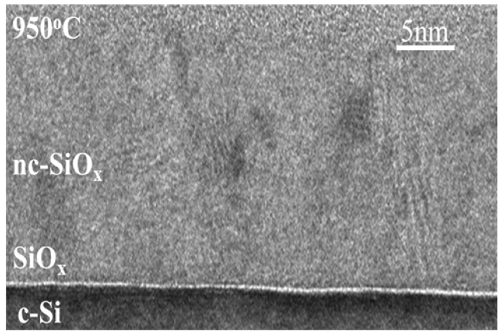
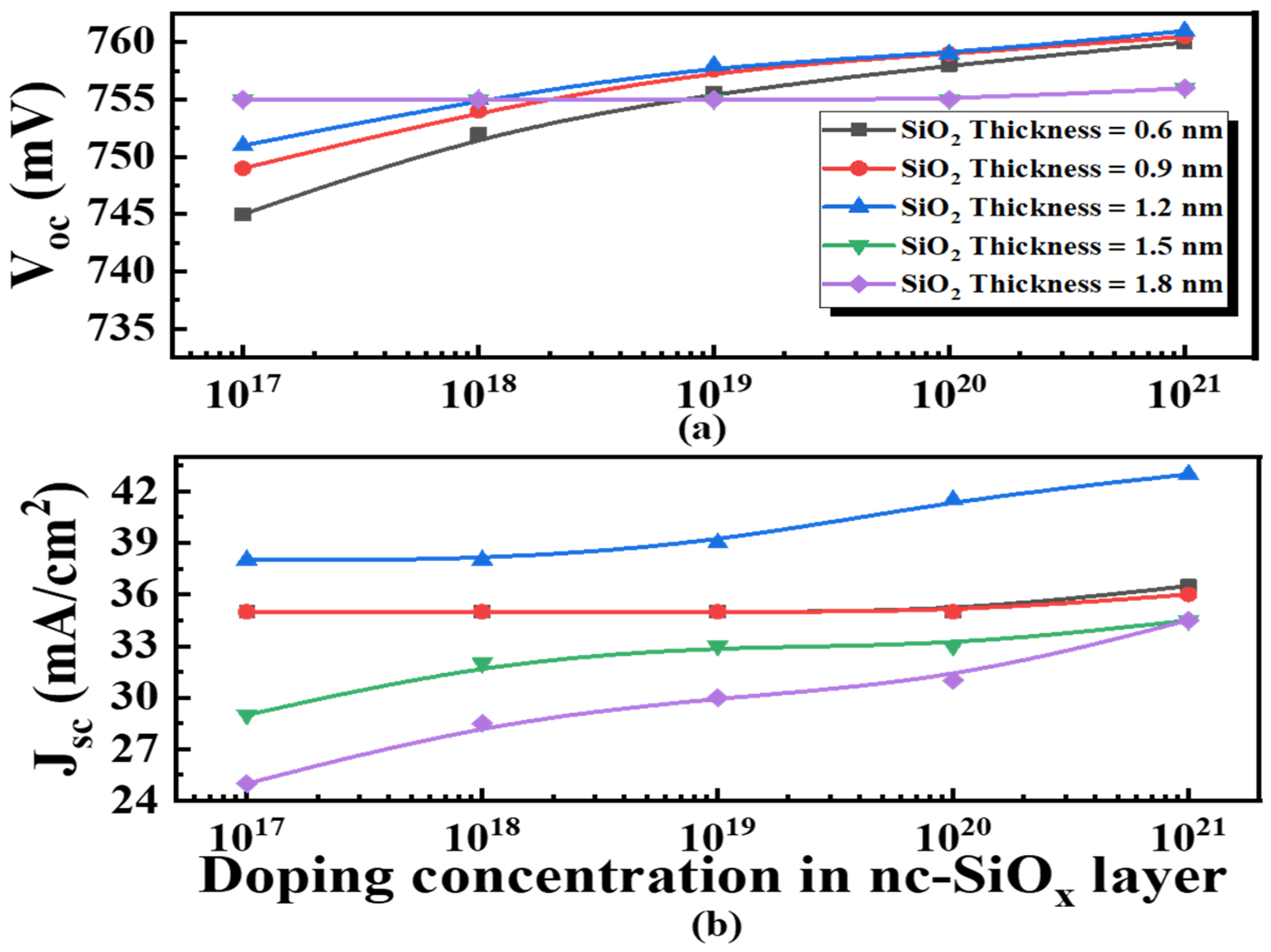
3.1. Electrical Properties of the nc-SiOx Layer

In order to optimize and enhance the efficiency of a solar cell, the electrical, as well as optical properties of the n-type nc-SiOx layer, can be varied. It can be applied to enhance carrier selectivity and rear side optical transmission, both of which are essentially significant in device operation. Our current research includes nc-SiOx material and its application in TOPCon solar cells as an optimized layer; where the goal is to provide the absorber layer with more light and ameliorate the selectivity of the carrier collection. A highly doped layer, as well as wide bandgap material, can assist with sharp band-bending, which enhances the carrier selectivity. Molybdenum-oxide, for instance, may be used as hole selective contacts. One of the key benefits of the nc-SiOx material is that the optical band-gap, or transparency, can be simply changed by various deposition conditions. The electrical conductivity was measuring the electrical (dark) conductivity (σ) in a planar electrode configuration (planar-conductivity), where current flows along the plane of the film, which we obtained around 1.1 × 10⁻¹ S/cm. Parallel with the electrical (dark) conductivity (σ), the activation energy (Ea) was measured and estimated to be around 0.04 eV. The refractive index (n) of the nc-SiOx films was estimated from spectroscopic ellipsometric measurements. The measured refractive index (n) ~2.9 at 600 nm indicates the excellent transparency of nc-SiOx. The characteristic of the nc-SiOx layer deposited on the ultrathin SiO2 passivation layer was shown by a cross-section transmission electron microscopy (TEM) image, as depicted in Figure 2. The thickness of the ultrathin SiO2 passivation layer was recorded as 1.2 nm. After thermal annealing at 950 °C, crystallization of the Si-rich region was further promoted, as shown in Figure 2 with their max grain sizes.

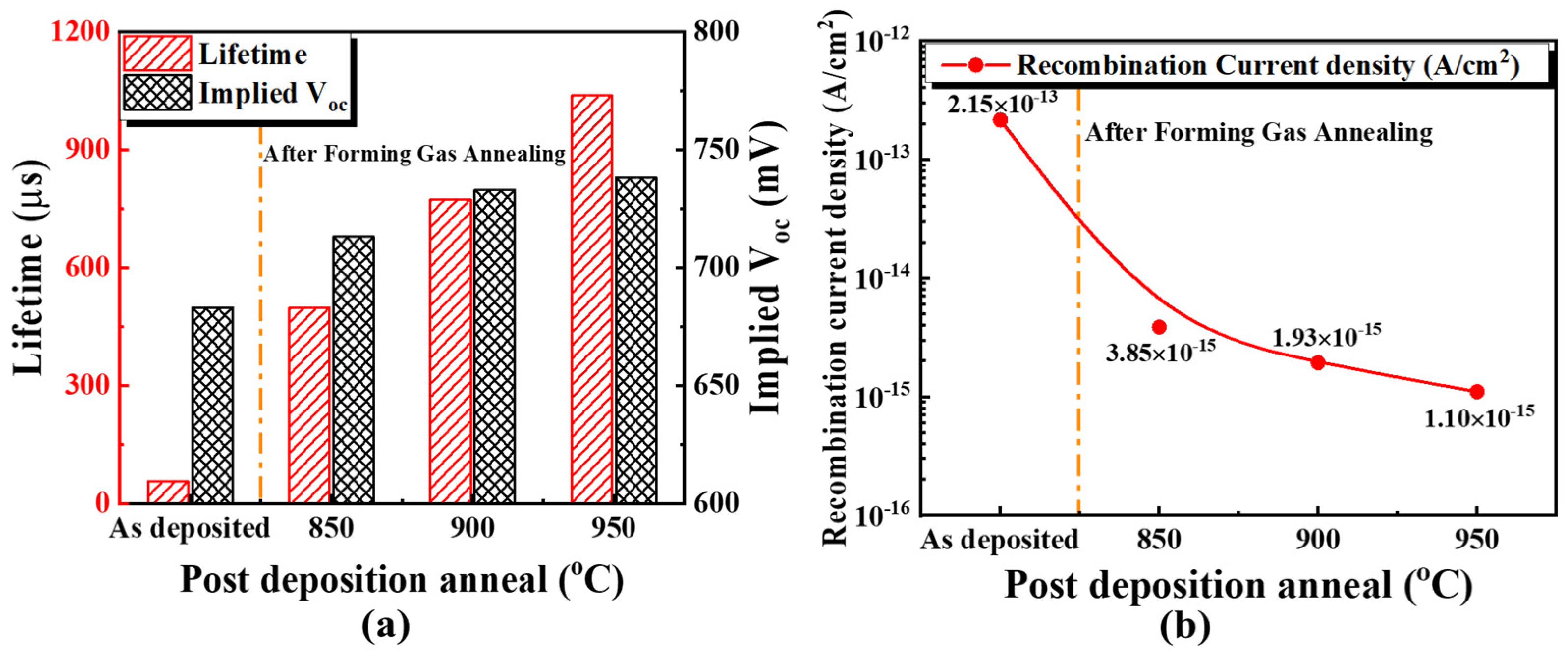
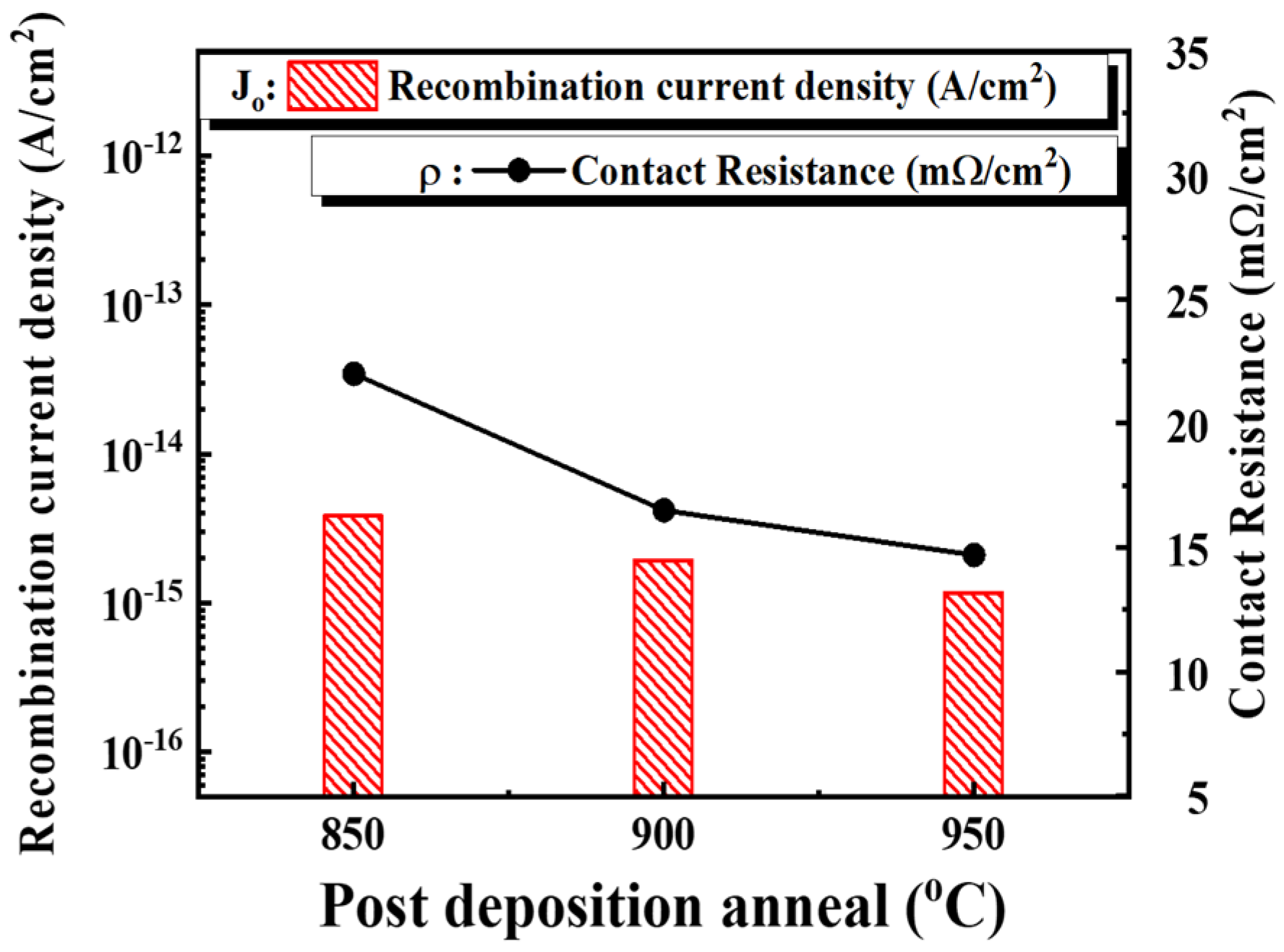
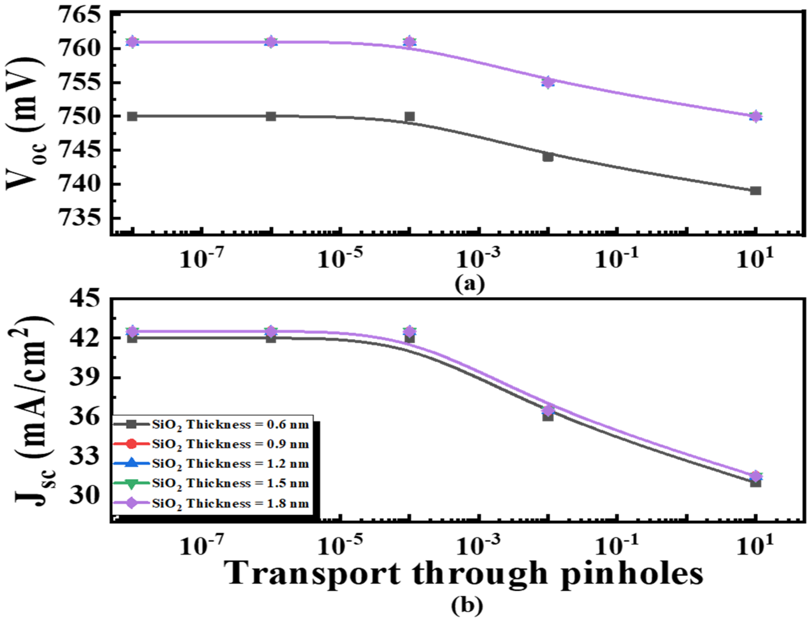
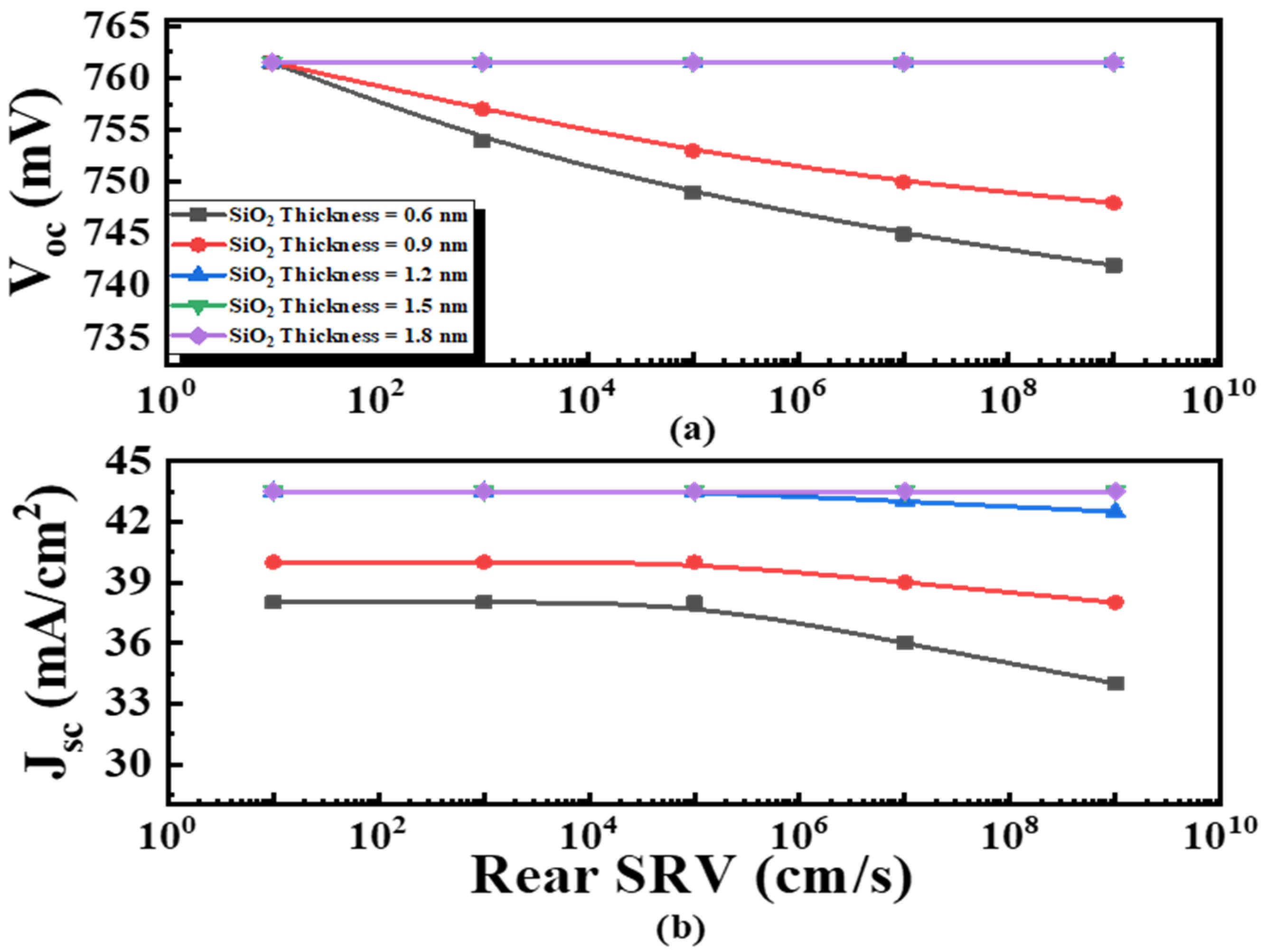
3.2. Analysis of Passivation Properties

Note that the implied open-circuit voltage (iVoc), derived from implicit current–voltage characteristic curves of the QSSPC, is an essential parameter to evaluate the overall performance of a silicon solar cell, as it reflects the quality of surface passivation and the lifetime bulk carrier. The iVoc of the double-sides symmetrical passivation structure, nc-SiOx/SiO2/n-type Si/SiO2/nc-SiOx layers, was studied exhaustively to estimate the surface passivation of the TOPCon structure. The iVoc can be described using Equation (3):
i V o c = k T q L n ( Δ n ( Δ n + N d o p n i 2 ) )
where Δn is the excess carrier density at one sun, k is the Boltzmann constant, T is the temperature, q is the elementary charge, Ndop is the bulk doping density, and ni is the intrinsic carrier concentration. Ndop and t of the wafer used for the calculation are 5 × 1015 cm−3 and 200 μm, respectively.
Note that the carrier lifetime (τeff), which can be measured experimentally in a given sample, is an effective parameter that encompasses several different recombination and transport mechanisms, including surface recombination. τeff derived from the implicit current–voltage characteristic curves of the QSSPC, is an essential parameter to evaluate the overall performance of a silicon solar cell. The τeff of the double-sides symmetrical passivation structure, nc-SiOx/SiO2/n-type Si/SiO2/nc-SiOx layers, was studied exhaustively to estimate the surface passivation of the TOPCon structure. The τeff can be described using Equation (4):
τ e f f = Δ n ( t ) G L ( t ) Δ n t
where GL(t) is the generation rate per unit volume.
The deposited 30 nm thick nc-SiOx sample was annealed at different temperatures in the range of 850–950 °C. As a result of the PDA, a substantial improvement was observed in the passivation characteristics after the PDA. As the thickness approached 30 nm, substantial improvements were observed in both the carrier lifetime (τeff) and implied open-circuit voltage (iVoc). Figure 3a depicts the τeff and iVoc of the 30 nm deposited sample at different post-deposition annealing temperatures (TPDA). We found more prominent results with the samples in terms of τeff and iVoc, as compared to the as-deposited sample, but in the case of the 950 °C temperature, a more notable lifetime, and iVoc of ~941 μs and ~737 mV, respectively, was observed. In the case of Figure 3b, we attempt to demonstrate the response of TPDA on the 30nm thick layer of the nc-SiOx in terms of recombination current density (Jo). The gradual decrease in Jo valued up to a Jo of 1.26 fA/cm2 was observed as the annealing temperature reaches 950 °C. At the annealing temperature in the range of 950 °C, increases in the τeff and iVoc, as well as the diminution in Jo, were observed compared to the as-deposited state of the nc-SiOx layer.
After FGA treatment for 2 h at 400 °C by using rapid thermal processing, the passivation characteristic of the symmetric structure increased further. After FGA treatment, the maximum lifetime was improved by up to 1 ms and the iVoc reached up to 738 mV, for the 30 nm thick nc-SiOx which represented in Figure 4a. Under this condition, a substantial reduction was observed in Jo up to 1.1 fA/cm2. A significant decrease in the interface defect density (Dit), could be a cause for the improved passivation after the FGA treatment. An increase in hydrogen activation on both sides of the tunnel oxide interface as well as the nc-SiOx layer was due to FGA treatment. This led to the best passivation with a 30 nm thick nc-SiOx layer which was annealed at 950 °C. The improved results of the passivation characteristics and lower Jo shows that this novel structure would produce a higher efficiency TOPCon cell. Figure 4a depicts meliorations in τeff and iVoc following FGA treatment for the 30 nm nc-SiOx deposited sample. Figure 4b depicts the change in Jo after the FGA at the same parameters as mentioned above. The Jo was found to be as low as ~1.1 fA/cm2 after FGA.
An improvement was observed at the SiOx/nc-SiOx passivated contact after thermal annealing at 950 °C and FGA treatment at 400 °C, yielding the lowest Jo and ρ values. Tunneling efficiency improved as Jo and ρ values decreased. Figure 5 depicts the Jo and ρ of the deposited samples at a 30 nm thickness of nc-SiOx as a function of TPDA. The melioration in Jo and lowest ρ value for the 30 nm SiOx/nc-SiOx passivated contact annealed at 950 °C, was outstanding compared to samples annealed at 850 °C and 900 °C. At a 30 nm thickness, the Jo up to 1.1 fA/cm2 and ρ up to 14.7 (mΩ/cm2) values decreased as the annealing temperature was raised to 950 °C. After comparing our results with those of other research groups such as Josua et al. [28], it was shown that we attained ameliorated passivation results. To ameliorate the TOPCon solar cell efficiency, nc-SiOx was applied in both studies; however, the differences lay with the layer thickness and deposition temperature as well as in the growth method of the SiOx. The novelty in our results arise from the different treatment steps and fabrication methods employed.

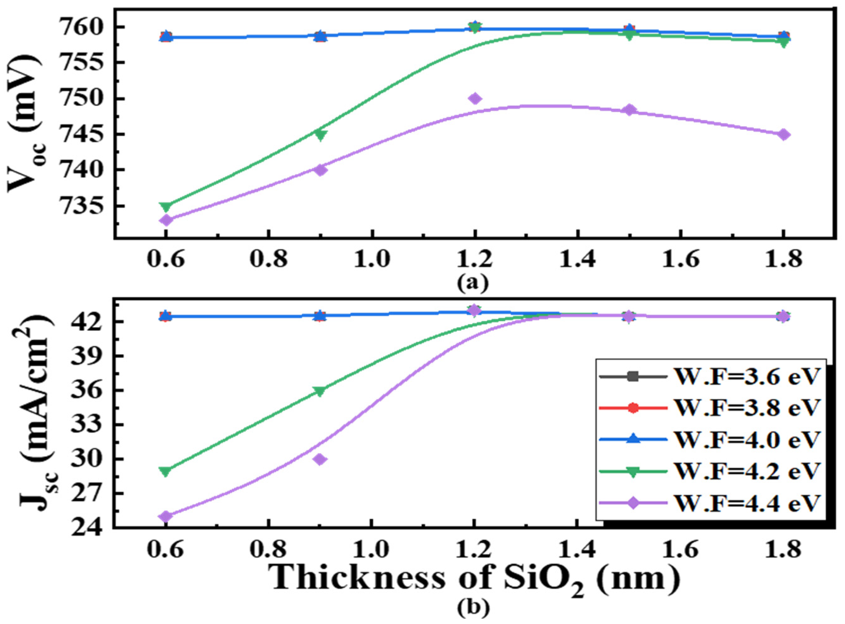
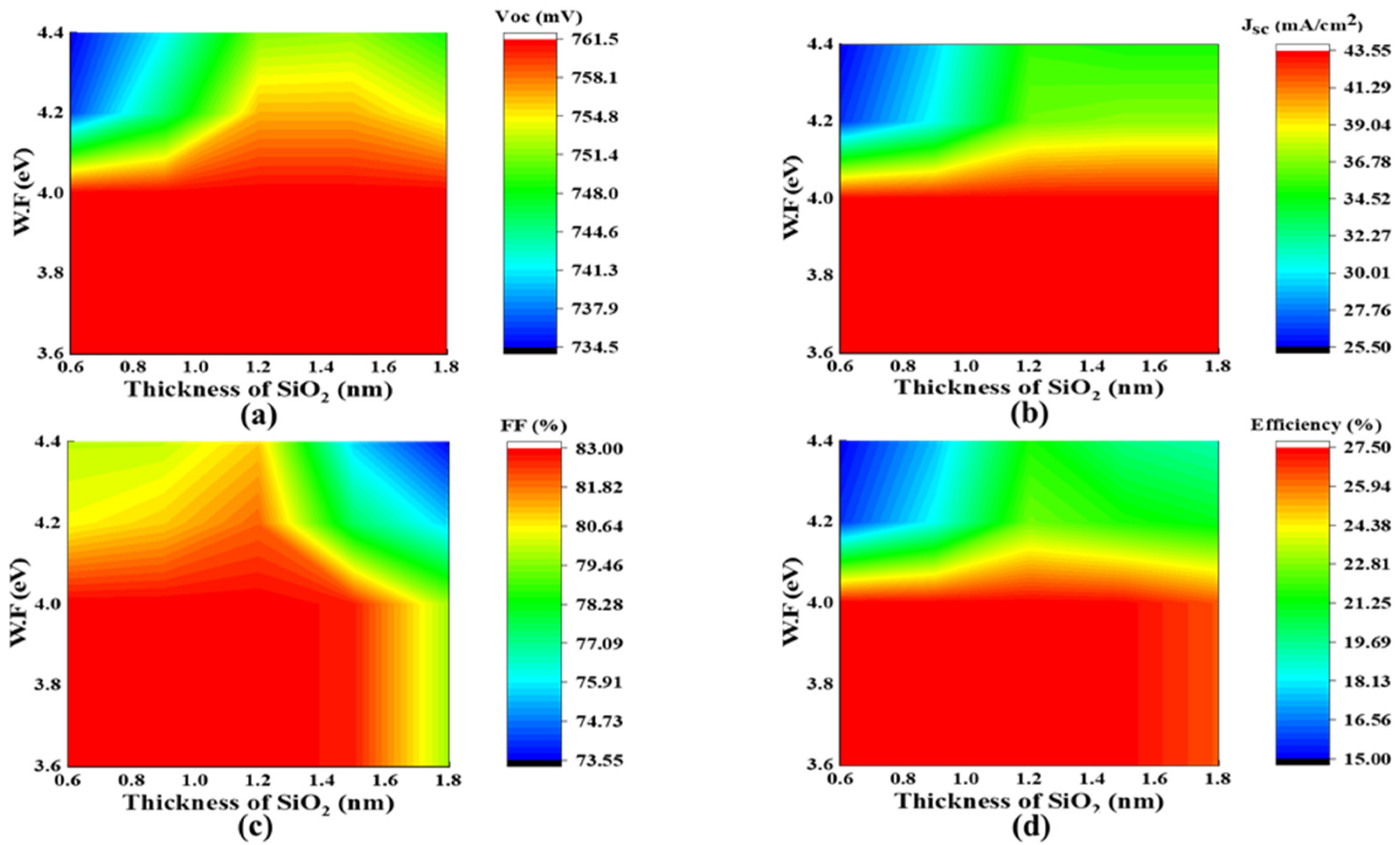
3.3. Path towards Cell Parameters Optimization

First, we examined the case when varying the thickness of nc-SiOx. From the results, we learned that TOPCon solar cell performance is affected by the nc-SiOx properties, such as the fabrication process and layer thickness, significantly. In this Section 3.3, we present a set of simulation results for the carrier transport in the TOPCon structure as used for the current–voltage measurement. Note that open circuit voltage (Voc), as well as short circuit current (Jsc), is derived from the current–voltage characteristics curve to assess the entire Si solar cell performance, because this indicates the achievement of the solar cell in terms of efficiency. The consequences regarding tunnel oxide thickness were investigated along with their work function, as depicted in Figure 6. Jsc was greatly improved by embedding a thin oxide layer, which was similar to the case of a nanocrystalline-based TOPCon structure [28]. Generally, Voc and Jsc increased gradually to the maximum value as the work function reduced and the oxide thickness increased. It should be note that the Jsc would drop down quickly as the tunnel oxide exceeded a certain thickness because of the invalidity of carrier tunneling (not shown in Figure 6); however, the Voc and Jsc showed the same characteristics at the work function range from 3.6 to 4.0 eV. The nc-SiOx layer, with a thickness of 30 nm, was interpreted as the model to elucidate this circumstance, for example, when the Voc increased from 733 to 760 mV through an increase of the thickness of the oxide ranging from 0.6 to 1.8 nm. Particular crystalline nanostructures with a 4.0 eV work function and a thickness of 30 nm exhibited better performance with the tunnel oxide of a 1.2 nm thickness. The champion performing Voc of the nc-SiOx TOPCon solar cell reached 760 mV, and the Jsc reached 43 mA/cm2 at a 1.2 nm thin tunnel oxide layer with up to a 4.0 eV work function, as shown in Figure 6a,b. The results of the Voc and Jsc, at a work function level of 3.6 eV, 3.8 eV, and 4.0 eV, respectively, show almost the same result. which is depicted in Figure 6a,b. This result suggests that this novel advanced TOPCon solar cell through an nc-SiOx layer with a superior tunnel oxide, attains magnificent surface passivation, which is competitive with an ordinary poly-Si TOPCon solar cell. Cheng et al. [29] reported on a TOPCon solar cell with a low-work function electron-selective-collection (ESC) as having a Voc of 735 (mV) and Jsc of 37 (mA/cm2), with an oxide layer over 0.8 nm and a work function range from 3.2 eV to 4.0 eV; however, in our novel TOPCon structure with the nc-SiOx layer, the results achieved up to 760 (mV) Voc and 43 (mA/cm2) Jsc with an oxide layer of ~1.2 nm and work function up to 4.0 eV. Moreover, a few practical problems that might hinder the development of an experimental, high-efficiency TOPCon solar cell are now discussed. The first and most critical issue is determining how to produce a thin, low-Dit, and low-Dph oxide layer. A wet, chemically grown oxide layer (such as hot HNO3) is often of poor quality, with a high density of interfacial defects. To eradicate the defects in these oxides, a high-temperature anneal of 800 °C to 1100 °C is necessary; however, the growth of the oxide thickness is a side effect of high-temperature anneals, e.g., only the 800 °C anneal can lead to an oxide of >2 nm that will decay the fill factor significantly. PECVD is a better tool for depositing a low-Dit oxide. Furthermore, it is challenging to maintain an oxide thickness of less than 2 nm and build a dense oxide layer with a low pinhole density using this approach. Thermal oxidation, which we adopted and detailed before in the experimental phase, has proven to be the most stable and probable contender among the remaining techniques for depositing a thin oxide.
Tunneling efficiency decreases as oxide thickness grows, but tunneling efficiency improves as doping concentration increases. Therefore, to obtain high performance and excellent tunneling current in the TOPCon cells, optimization is necessary. Various device parameters were observed for an oxide thickness ranging from 0.6 nm to 1.8 nm and an nc-SiOx doping concentration from 1 × 10¹⁷ to 1 × 1021 cm−3, as shown in Figure 7. Due to surface recombination, the Voc was low with a thick oxide layer and low doping density. As the doping density increased, Voc increased as well as the Jsc. Voc is a lead parameter to evaluate the device performance because it is computed through a current–voltage curve. Comparatively, similar trends were realized in the Voc, as demonstrated in Figure 7a. The Voc was minimized to 745 mV for the architecture with a SiO2 layer thickness of 0.6 nm. The maximum Voc value was enhanced up to the 761 mV by contributing a right oxide and nc-SiOx stack layer with proper doping level, which indicated that a TOPCon solar cell has the huge capacity to accomplish a quite high Voc, as long as the front-sided surface recombination is depressed. Figure 7b shows that Jsc reached up to 43 mA/cm2 for the architecture with a SiO2 layer of 1.2 nm. Jsc was diminished to an inferior value of 25 mA/cm2 by using the nc-SiOx layer under a low doping concentration of approximately 1 × 1017 cm−3. Similarly, the Jsc was diminished to about 25 mA/cm2 by employing a tunnel oxide layer along with a thickness beyond 1.8 nm. When the thickness of the tunnel oxide was near 1.2 nm, the Jsc depicted slight sensitivity to the nc-SiOx doping level, and exclusively once the doping concentration was more prominent with 1 × 1021 cm−3. This required that the Jsc be affected through a number of components, comprising the adopted parameters and mathematics model, such as wafer quality, doping concentration of the wafer, SRV, and doping of the nc-SiOx layer, that can account for the various findings computed by several researchers; however, the physics behind the simulation could not be modified. Zeng et al. [25] reported on a TOPCon solar cell with the n+-Si layer having a Voc of 737 (mV) and Jsc of 37 (mA/cm2), with an oxide layer of ~1 nm and a doping level (Nd) of 1 × 1019 cm−3. However, in our novel TOPCon structure with an nc-SiOx layer, the results reached up to 761 (mV) Voc and 43 (mA/cm2) Jsc, respectively, with an oxide layer of ~1.2 nm and a doping level (Nd) of 1 × 1021 cm−3.
As the oxide thickness rises, the tunneling efficiency falls, but as the bulk defect density increases, the tunneling efficiency drops. The various device parameters were observed for oxide thickness from 0.6 nm to 1.8 nm, and nc-SiOx bulk defect density from 1 × 10¹⁷ to 1 × 1021 cm−3, as shown in Figure 8a,b. As demonstrated in Figure 8a, the Voc decreased by 0.52 percent from 761 to 757 mV at a 1.2 nm oxide layer due to an increase in the bulk-defect density ranges from 1 × 10¹⁷ to 1 × 1021 cm3. Since the oxide thickness began to increase from 1.2 nm, the Voc reached a minimum value of approximately 755 mV at the work function of 4.0 eV for all the oxide layers. The studies revealed that a sufficient oxide thickness might tolerate the negative effects of defects while still producing satisfactory outcomes. The Jsc impact of the oxide thickness under a bulk-defect density in the nc-SiO2 layer is shown in Figure 8b. Cell performance and surface passivation were diminished by the increase in oxide thickness. Luckily, after introducing a proper thin oxide around 1.2 nm, the Jsc turned less sensitive with the nc-SiO2 thickness. In particular, the Jsc reached the highest value of about 43 mA/cm2 with regards to an oxide thickness of around 1.2 nm. According to the findings, it was possible to achieve the maximum Jsc by inserting an appropriate thin tunnel oxide that eliminated the influence of the defects.
The values of the tunnel oxide layers’ interface trap density (Dit) were incorporated into the AFORS HET simulation, the results of which are presented in Figure 9. The effects of SiO2 quality on the surface passivation and cell performance are investigated using Dit characteristics. It should be noted that Dit is fixed within the interface of the Si wafer and the oxide layer. As presented in Figure 9, the Voc and Jsc of the complete structure decreased with the increase of Dit. The Dit was ranging from 1 × 108 cm−2 eV−1 to 1 × 1012 cm−2 eV−1. A more prominent Jsc, Voc, and overall cell efficiency were achieved with a minimum Dit value. The main factor which affected the conversion efficiency was the Voc (761.5 mV) for the minimal Dit (1 × 108 cm−2 eV−1) at a perfect thin oxide layer of around 1.2 nm, as presented in Figure 9a. The rear electrode directly contacted the back-surface field in the passivated emitter and rear cell (PERC) solar cells, whereas the carrier on the rear side of the structure passed to the nc-SiOx layer through a tunneling mechanism in the passivated contact. Therefore, the tunneling oxide under a minimal Dit value resulted in an ameliorated conversion efficiency. The highest simulated value Jsc of 43.5 mA/cm2 was accomplished when the Dit had a minimal value of approximately 1 × 108 cm−2 eV−1 at a perfect thin oxide layer of around 1.2 nm, as shown in Figure 9b. The Jsc kept to above a Jsc of 43.5 mA/cm2 at a Dit value of 1 × 108 cm−2 eV−1, while it decreased to 29 mA/cm2 when the Dit rose to 1 × 1012 cm−2 eV−1. Cheolmin Park et al. [30] reported on a TOPCon solar cell having a Voc of 712 (mV) and Jsc of 41.30 (mA/cm2) with a Dit value of 1 × 1010 cm−2 eV−1. In our novel TOPCon structure with an nc-SiOx layer, the simulation results reached up to Voc 761.5 mV and Jsc 43.5 mA/cm2 with an oxide layer of ~1.2 nm plus a Dit value of 1 × 108 cm−2 eV−1. Bert et al. [31] published an experimentally based result for a low Dit value of up to 7 × 1011 cm−2 eV−1 that considered a tunnel oxide’s strong passivation ability. Wet chemical oxidation procedures were used to synthesize this tunnel oxide.
From the carrier transport study, we learned that in addition to the tunneling, the transport through pinholes affected the J-V characteristics of the junction significantly. Hence, it is convincing to suppose that carrier transport through pinholes could influence the performance of real TOPCon solar cells. The existence of a high-density oxide pinhole was also harmful to surface passivation, as presented in Figure 10. Therefore, the TOPCon solar cell performance, considering the probability of carrier transport through pinholes ranging from 10−8 to101, was studied with five different thicknesses of the SiOx layer ranging from 0.6 nm, 0.9 nm, 1.2 nm, 1.5 nm, and 1.8 nm. Figure 10a,b shows the performance parameters considering the transport through pinholes. In such a case, the thin SiOx layer furnished quite a high tunneling current to permit a majority of the photo-carrier. A lower fill factor (FF) was found without transport via pinholes; a modest amount of transport through the pinholes increased the FF; too much transport through the pinholes decreased the FF, Voc, and Jsc considerably. Tunneling transport in the TOPCon solar cells with a comparably thick SiOx (1.5 nm and 1.8 nm) could not provide enough transport channels, limiting the current flow, and leading to a high series resistance (Rs) as well as an inferior FF. Through the addition of the pinhole mitigated transport at a pinhole density ranging from 10−8 to10−6, the FF rose, Rs diminished, and thus, overall efficiency was enhanced. In the region of prominent pinhole transport (>10−3), the performance parameters (Voc, and Jsc) began to decline at all thicknesses of the SiOx layer and resulted in a diminishing efficiency. When pinholes were involved, apart from the transport through tunneling, the carriers were also transported through the pinholes, which diminished the Rs, and hence, ameliorated the FF as well as the efficiency. Nevertheless, the results showed that raising the pinhole transport adds a shunt path as well as decreases the carrier built up within the junction in a context of an open circuit condition, thus diminishing the Voc. Moreover, the excess pinholes could decrease the passivation quality, raise the interface recombination, and deteriorate the cell’s performance. With the help of a simulation study, it was shown that an appropriate amount of pinholes in the thin SiO2 passivation layer is required for prominent efficiency of the TOPCon solar cells through a thick SiO2, namely, 1.2 nm, which is a necessary for ameliorating the Voc as well as Jsc in real solar cells. The Voc and Jsc values for SiO2 thicknesses of 1.2 nm, 1.5 nm, and 1.8 nm, respectively, indicate approximately the same results, and again in the case of SiO2 thicknesses of 0.6 nm and 0.9 nm, which are illustrated in Figure 10a,b. Zhang et al. [32] reported on a TOPCon solar cell with poly-Si having a Voc of 735 (mV) and Jsc of 37.7 (mA/cm2), with an oxide layer of 1.4 nm and pinhole density of 10−6~10−5; however, in our novel TOPCon structure with an nc-SiOx layer, the results reached up to a Voc of 761 mV and Jsc of 42.5 mA/cm2, with an oxide thickness of ~1.2 nm and pinhole density of 1 × 10⁻⁴.
The tunnel oxide increased the passivation quality at the rear, decreasing the current recombination density [33]. A thicker oxide layer increased the bandgap between electrons and holes at the quasi-fermi levels, thus increasing the Voc and reducing the leak current to almost zero [34]. On increasing the width of the thin oxide layer, the effect of SRV reduced, as observed in Figure 11. With the thinner oxide layer (~0.6 nm thick), there was a substantial decline in Voc from 761.5 to 742 mV with the rear SRV from 1 × 101 to 1 × 109 cm/s, thereby the Jsc was decreased from 38 to 34 mA/cm2. From the increase in oxide thickness, the SRV limiting effect was released and, therefore, the Voc as well as the Jsc improved. With the thickness above 1.2 nm in Figure 11a, the SRV impact over Voc was diminished. In Figure 11b, the tunneling oxide thickness above 1.2 nm was essential for excellent passivation, where the SRV did not affect the cell performance. The cause of that decline can be understood with the dark J–V characteristics, with a diminishing tunneling current density (15–16 times) with every single increase of 0.2 nm oxide thickness [25], as well as a rise in parasitic resistance. As a result of these impressions, the efficiency of the structure rose to a 1.2 nm thickness, although, it then began to diminish. Through a rise in the oxide thickness, a diminishing tunneling efficiency was observed, and the conversion efficiency should diminish because of a reduced current passage. Meanwhile, the oxide layer decreased recombination because of the best passivation outcome as well as the selective passage of the charge carrier by means of tunneling. The reduction in tunneling efficiency was controlled by a decrease in recombination; consequently, we saw an overall increase in conversion efficiency. To limit the influence of SRV on the solar cell’s efficiency, the tunnel oxide layer thickness should be kept between 0.8 and 1.2 nm. Niraj et al. [26] reported on a TOPCon solar cell with n+ poly-Si having a Voc of 761 (mV) and Jsc of 43.2 (mA/cm2), with an oxide layer of ~1 nm and SRV value of 1 × 104 cm/s; however, in our novel TOPCon structure with an nc-SiOx layer, the results reached up to 761.5 (mV) Voc and 43.5 (mA/cm2) Jsc, respectively, with an oxide layer of ~1.2 nm and an SRV value of 1 × 101.

3.4. TOPCon Solar Cell Achievement

Figure 12a–d shows the consequences of the thickness of the oxide layer as well as the oxide layer’s work function on the device’s performances, whose default parameters are included in Table 1. Generally, Voc and Jsc have the maximum value at a work function below 4.0 eV and progressively decrease with an increase in the work function of the nc-SiOx layer. It was observed that the Jsc would drop rapidly as the tunnel oxide surpassed a specific thickness due to the deficiency of carrier tunneling. The fill factor was also affected by oxide thickness because the tunnel current diminished by ~15 times with every 0.2 nm increase in the thickness of the oxide. The highest efficiency of an nc-SiOx-based TOPCon solar cell, 27.49%, was accomplished with an oxide layer of ~1.2 nm; however, a practical problem that may obstruct the preparation of a high efficiency nc-SiOx based TOPCon solar cell remains. The critical complication concerns how to develop a low-Dit as well as a low pinhole oxide layer with an adjustable thickness. An oxide layer is synthesized using a wet chemical method (such as hot HNO3) with an immense density of interfacial defects. The higher annealing temperature varies from 800 °C to 1100 °C [10,11] and is needed to exclude the oxide defects and anneal the nc-SiOx layer.

4. Conclusions

In conclusion, we presented a TOPCon optimization by applying the numerical tool, AFORS-HET, as well as an experimental method. On the base of the model, we examined the carrier selectivity towards passivated electron contacts overall. Our work furnished a comprehensive understanding of tunnel oxide, rear-SRV, doping density, as well as of the design of TOPCon solar cells. Our experimental results show that the higher Jo and iVoc reached up to ~1.1 fA/cm2 and 738 mV, respectively. As far as the simulation is concerned, the high-quality tunnel oxide with a work function of 4.0 eV as well as a thickness of 1.2 nm is necessary for sensible carrier transport and field passivation. The champion results of a Voc of 761.5 mV and Jsc of 43.5 mA/cm2 were achieved with the novel TOPCon solar cell simulation. Representing a superior oxide layer with a low Dit range of 1 × 108 cm−2 eV−1, as well as a low Dph below 1 × 10⁻⁸, was essential for attaining the maximum simulated values. The higher concentration of doping in the nc-SiOx layer was beneficial for ameliorating carrier-collection, which is useful as it enables a manufacture to be more tolerant of a thicker oxide. Furthermore, this is also promising for mass production. In a nutshell, it is possible to monitor the above-mentioned parameters, for instance, oxide thickness, doping concentration, rear-SRV, Dit, and Dph, which can then be controlled, therefore, we consider that a high-efficiency output is achievable. With will-designed manufacturing, TOPCon solar cells are moving closer to achieving their theoretically predicted efficiency.

Author Contributions

Conceptualization, M.Q.K. and E.-C.C.; formal analysis, S.Q.H. and M.A.Z.; investigation, M.Q.K. and D.P.P.; writing—original draft preparation, M.Q.K.; writing—review and editing, E.-C.C. and S.Q.H.; supervision, E.-C.C. and J.Y.; project administration, E.-C.C. and J.Y.; funding acquisition, J.Y. All authors have read and agreed to the published version of the manuscript.

Funding

This research was supported by grants from the New and Renewable Energy Technology Development Program of the Korea Institute of Energy Technology Evaluation and Planning (KETEP) funded by the Korean Ministry of Trade, Industry and Energy (MOTIE) (Project No. 20203030010310, 20213030010240).

Institutional Review Board Statement

Not applicable.

Informed Consent Statement

Not applicable.

Data Availability Statement

All the data available in the manuscript.

Conflicts of Interest

The authors declare no conflict of interest.

References

  1. Feldmann, F.; Bivour, M.; Reichel, C.; Hermle, M.; Glunz, S.W. A passivated rear contact for high-efficiency n-type silicon solar cells enabling high Vocs and FF > 82%. In Proceedings of the 28th European PV Solar Energy Conference and Exhibition, Villepinte, France, 30 September–4 October 2013. [Google Scholar]
  2. Feldmann, F.; Bivour, M.; Reichel, C.; Hermle, M.; Glunz, S.W. Passivated rear contacts for high-efficiency n-type Si solar cells providing high interface passivation quality and excellent transport characteristics. Sol. Energy Mater. Sol. Cells 2014, 120, 270–274. [Google Scholar] [CrossRef]
  3. Feldmann, F.; Bivour, M.; Reichel, C.; Steinkemper, H.; Hermle, M.; Glunz, S.W. Tunnel oxide passivated contacts as an alternative to partial rear contacts. Sol. Energy Mater. Sol. Cells 2014, 131, 46–50. [Google Scholar] [CrossRef]
  4. Feldmann, F.; Simon, M.; Bivour, M.; Reichel, C.; Hermle, M.; Glunz, S.W. Efficient carrier-selective p-and n-contacts for Si solar cells. Sol. Energy Mater. Sol. Cells 2014, 131, 100–104. [Google Scholar] [CrossRef]
  5. Reichel, C.; Feldmann, F.; Müller, R.; Moldovan, A.; Hermle, M.; Glunz, S.W. Interdigitated back contact silicon solar cells with tunnel oxide passivated contacts formed by ion implantation. In Proceedings of the 29th European PV Solar Energy Conference and Exhibition, Amsterdam, The Netherlands, 22–26 September 2014. [Google Scholar]
  6. Moldovan, A.; Feldmann, F.; Kaufmann, K.; Richter, S.; Werner, M.; Hagendorf, C.; Zimmer, M.; Rentsch, J.; Hermle, M. Tunnel oxide passivated carrier-selective contacts based on ultra-thin SiO2 layers grown by photo-oxidation or wet-chemical oxidation in ozonized water. In Proceedings of the 2015 IEEE 42nd Photovoltaic Specialist Conference (PVSC), New Orleans, LA, USA, 14–19 June 2015; pp. 1–6. [Google Scholar]
  7. Yan, D.; Cuevas, A.; Bullock, J.; Wan, Y.; Samundsett, C. Phosphorus-diffused polysilicon contacts for solar cells. Sol. Energy Mater. Sol. Cells 2015, 142, 75–82. [Google Scholar] [CrossRef]
  8. Yan, D.; Cuevas, A.; Wan, Y.; Bullock, J. Passivating contacts for silicon solar cells based on boron-diffused recrystallized amorphous silicon and thin dielectric interlayers. Sol. Energy Mater. Sol. Cells 2016, 152, 73–79. [Google Scholar] [CrossRef]
  9. Tao, Y.; Upadhyaya, V.; Chen, C.W.; Payne, A.; Chang, E.L.; Upadhyaya, A.; Rohatgi, A. Large area tunnel oxide passivated rear contact n-type Si solar cells with 21.2% efficiency. Prog. Photovolt. Res. Appl. 2016, 24, 830–835. [Google Scholar] [CrossRef]
  10. Peibst, R.; Larionova, Y.; Reiter, S.; Turcu, M.; Brendel, R.; Tetzlaff, D.; Krügener, J.; Wietler, T.; Höhne, U.; Kähler, J. Implementation of n+ and p+ poly junctions on front and rear side of double-side contacted industrial silicon solar cells. In Proceedings of the 32nd European Photovoltaic Solar Energy Conference and Exhibition, München, Germany, 21–24 June 2016; pp. 323–327. [Google Scholar]
  11. Moldovan, A.; Feldmann, F.; Krugel, G.; Zimmer, M.; Rentsch, J.; Hermle, M.; Roth-Fölsch, A.; Kaufmann, K.; Hagendorf, C. Simple cleaning and conditioning of silicon surfaces with UV/ozone sources. Energy Procedia 2014, 55, 834–844. [Google Scholar] [CrossRef]
  12. Richter, S.; Kaufmann, K.; Naumann, V.; Werner, M.; Graff, A.; Großer, S.; Moldovan, A.; Zimmer, M.; Rentsch, J.; Bagdahn, J. High-resolution structural investigation of passivated interfaces of silicon solar cells. Sol. Energy Mater. Sol. Cells 2015, 142, 128–133. [Google Scholar] [CrossRef]
  13. Ge, H. Development of High Efficiency SHJ/Poly-Si Passivating Contact Hybrid Solar Cells. Master’s Thesis, Delft University of Technology, Delft, The Netherlands, 2017. [Google Scholar]
  14. Glunz, S.; Preu, R.; Biro, D. Crystalline silicon solar cells: State-of-the-art and future developments. Compr. Renew. Energy 2012, 1, 353–387. [Google Scholar]
  15. Steinkemper, H.; Hermle, M.; Glunz, S.W. Comprehensive simulation study of industrially relevant silicon solar cell architectures for an optimal material parameter choice. Prog. Photovolt. Res. Appl. 2016, 24, 1319–1331. [Google Scholar] [CrossRef]
  16. Steinkemper, H.; Feldmann, F.; Bivour, M.; Hermle, M. Numerical simulation of carrier-selective electron contacts featuring tunnel oxides. IEEE J. Photovolt. 2015, 5, 1348–1356. [Google Scholar] [CrossRef]
  17. Steinkemper, H.; Feldmann, F.; Bivour, M.; Hermle, M. Theoretical investigation of carrier-selective contacts featuring tunnel oxides by means of numerical device simulation. Energy Procedia 2015, 77, 195–201. [Google Scholar] [CrossRef]
  18. Mitra, S.; Ghosh, H.; Saha, H.; Ghosh, K. Recombination Analysis of Tunnel Oxide Passivated Contact Solar Cells. IEEE Trans. Electron Devices 2019, 66, 1368–1376. [Google Scholar] [CrossRef]
  19. Fell, A.; Schön, J.; Müller, M.; Wöhrle, N.; Schubert, M.C.; Glunz, S.W. Modeling edge recombination in silicon solar cells. IEEE J. Photovolt. 2018, 8, 428–434. [Google Scholar] [CrossRef]
  20. Stephens, A.; Aberle, A.; Green, M. Surface recombination velocity measurements at the silicon–silicon dioxide interface by microwave-detected photoconductance decay. J. Appl. Phys. 1994, 76, 363–370. [Google Scholar] [CrossRef]
  21. Luke, K.L.; Cheng, L.J. Analysis of the interaction of a laser pulse with a silicon wafer: Determination of bulk lifetime and surface recombination velocity. J. Appl. Phys. 1987, 61, 2282–2293. [Google Scholar] [CrossRef]
  22. Sproul, A. Dimensionless solution of the equation describing the effect of surface recombination on carrier decay in semiconductors. J. Appl. Phys. 1994, 76, 2851–2854. [Google Scholar] [CrossRef]
  23. Brody, J.; Rohatgi, A. Analytical approximation of effective surface recombination velocity of dielectric-passivated p-type silicon. Solid-State Electron. 2001, 45, 1549–1557. [Google Scholar] [CrossRef]
  24. Kim, S.; Park, J.; Phong, P.D.; Shin, C.; Iftiquar, S.; Yi, J. Improving the efficiency of rear emitter silicon solar cell using an optimized n-type silicon oxide front surface field layer. Sci. Rep. 2018, 8, 10657. [Google Scholar] [CrossRef] [PubMed]
  25. Zeng, Y.; Tong, H.; Quan, C.; Cai, L.; Yang, Z.; Chen, K.; Yuan, Z.; Wu, C.-H.; Yan, B.; Gao, P. Theoretical exploration towards high-efficiency tunnel oxide passivated carrier-selective contacts (TOPCon) solar cells. Sol. Energy 2017, 155, 654–660. [Google Scholar] [CrossRef]
  26. Anand, N.; Kale, P. Optimization of TOPCon Structured Solar Cell Using AFORS-HET. Trans. Electr. Electron. Mater. 2021, 22, 160–166. [Google Scholar] [CrossRef]
  27. Lancaster, K.; Großer, S.; Feldmann, F.; Naumann, V.; Hagendorf, C. Study of pinhole conductivity at passivated carrier-selected contacts of silicon solar cells. Energy Procedia 2016, 92, 116–121. [Google Scholar] [CrossRef]
  28. Stuckelberger, J.; Nogay, G.; Wyss, P.; Jeangros, Q.; Allebé, C.; Debrot, F.; Niquille, X.; Ledinsky, M.; Fejfar, A.; Despeisse, M. Passivating electron contact based on highly crystalline nanostructured silicon oxide layers for silicon solar cells. Sol. Energy Mater. Sol. Cells 2016, 158, 2–10. [Google Scholar] [CrossRef] [Green Version]
  29. Quan, C.; Zeng, Y.; Wang, D.; Liao, M.; Tong, H.; Yang, Z.; Yuan, Z.; Gao, P.; Yan, B.; Chen, K. Computational analysis of a high-efficiency tunnel oxide passivated contact (TOPCon) solar cell with a low-work-function electron-selective-collection layer. Sol. Energy 2018, 170, 780–787. [Google Scholar] [CrossRef]
  30. Park, C.; Balaji, N.; Ahn, S.; Park, J.; Cho, E.-c.; Yi, J. Effects of tunneling oxide defect density and inter-diffused carrier concentration on carrier selective contact solar cell performance: Illumination and temperature effects. Sol. Energy 2020, 211, 62–73. [Google Scholar] [CrossRef]
  31. Stegemann, B.; Balamou, P.; Lussky, T.; Gad, K.M.; Vössing, D.; Kasemann, M.; Angermann, H. Passivation of Crystalline Silicon Wafers by Ultrathin Oxide Layers: Comparison of Wet-chemical, Plasma and Thermal Oxidation Techniques. In Proceedings of the 2018 IEEE 7th World Conference on Photovoltaic Energy Conversion (WCPEC)(A Joint Conference of 45th IEEE PVSC, 28th PVSEC & 34th EU PVSEC), Waikoloa, HI, USA, 10–15 June 2018; pp. 2779–2782. [Google Scholar]
  32. Zhang, Z.; Zeng, Y.; Jiang, C.-S.; Huang, Y.; Liao, M.; Tong, H.; Al-Jassim, M.; Gao, P.; Shou, C.; Zhou, X. Carrier transport through the ultrathin silicon-oxide layer in tunnel oxide passivated contact (TOPCon) c-Si solar cells. Sol. Energy Mater. Sol. Cells 2018, 187, 113–122. [Google Scholar] [CrossRef]
  33. Kale, A.S.; Nemeth, W.; Harvey, S.P.; Page, M.; Young, D.L.; Agarwal, S.; Stradins, P. Effect of silicon oxide thickness on polysilicon based passivated contacts for high-efficiency crystalline silicon solar cells. Sol. Energy Mater. Sol. Cells 2018, 185, 270–276. [Google Scholar] [CrossRef]
  34. Grübel, B.; Cimiotti, G.; Arya, V.; Feldmann, F.; Steinhauser, B.; Kluska, S.; Glatthaar, M. Plated Ni/Cu/Ag for TOPCon solar cell metallization. In Proceedings of the 36th European Photovoltaic Solar Energy Conference, Marseille, France, 9–13 September 2019; pp. 1–5. [Google Scholar]
Figure 1. (a) Symmetric structure for measuring passivation characteristics, (b) graphical depiction of the TOPCon solar cell and (c) the schematic band diagram of the tunnel oxide passivating contact structure.
Applsci 12 00392 g001
Figure 2. Cross-section TEM images of nc-SiOx and ultrathin (~1.2 nm) SiO2 layer.
Applsci 12 00392 g002
Figure 3. (a) Minority carrier lifetime and implied open-circuit voltage as functions of TPDA at 30 nm nc-SiOx layer thickness. (b) Recombination current density as a function of TPDA.
Applsci 12 00392 g003
Figure 4. (a) Improvement in minority carrier lifetime and implied open-circuit voltage as a function of TPDA and FGA. (b) Improvement in rear recombination current density as a function of TPDA and FGA.
Applsci 12 00392 g004
Figure 5. Improvements in recombination current density and contact resistance after FGA annealing of the annealed nc-SiOx layer.
Applsci 12 00392 g005
Figure 6. Effect of oxide thickness (0.6–1.8 nm) with oxide work function (3.6–4.4 eV) on (a) Voc and (b) Jsc on the TOPCon solar cell.
Applsci 12 00392 g006
Figure 7. Effect of donor concentration (1 × 10¹⁷–1 × 1021 cm−3) with various oxide thicknesses (0.6–1.8 nm) on (a) Voc and (b) Jsc on the TOPCon solar cell.
Applsci 12 00392 g007
Figure 8. Effect of various bulk-defect density (1 × 10¹⁷–1 × 1021 cm−3) with various oxide thicknesses (0.6–1.8 nm) on (a) Voc and (b) Jsc on the TOPCon solar cell.
Applsci 12 00392 g008
Figure 9. Effect of various interface trap densities (1 × 10⁸–1 × 1012 cm−2/eV) with various oxide thicknesses (0.6–1.8 nm) on (a) Voc and (b) Jsc on the TOPCon solar cell.
Applsci 12 00392 g009
Figure 10. Effect of pinholes density (1 × 10⁻⁷–1 × 101) with various oxide thicknesses (0.6–1.8 nm) on (a) Voc and (b) Jsc on the TOPCon solar cell.
Applsci 12 00392 g010
Figure 11. Effect of rear-SRV (1 × 101–1 × 109 cm/s) with various oxide thickness (0.6–1.8 nm) on (a) Voc and (b) Jsc on the TOPCon solar cell.
Applsci 12 00392 g011
Figure 12. Effect of the oxide thickness (0.6–1.8 nm) and oxide work function (3.6–4.4 eV) on (a) Voc, (b) Jsc, (c) FF, and (d) efficiency on the TOPCon solar cell.
Applsci 12 00392 g012
Table 1. Simulation Parameters for TOPCon Solar Cell.
LayersDefault Parameter
SiNx dielectrict = 70 nm
Front contact boundaryStandard texture surface (54.74°), w/o absorption loss, flat band
Front contactMS Schottky contact model, SRV = 10 cm/s (assuming good passivation)
P+-type Si layert = 0.3 µm, Na = 2 × 10²° cm−3, lifetime setting: 1 μs
n-type c-Si layert = 150 µm, Nd = 5.0 × 1016 cm−3, lifetime setting: 1 × 10⁵ μs (without bulk defect)
Interface: SiOxChi = 1.0 eV, Eg = 8.9 eV, dk = 3.9, me = 0.98, mh = 0.49, Dph = 0
nc-SiOx Si layert = 30 µm, Nd = 1 × 1017 cm−3, lifetime setting: 50 μs
Rear contactMS Schottky contact model, SRV = 10 cm/s
Rear contact boundaryA plane surface, w/o absorption loss, flat band
Ag electrodet = 1 µm
Publisher’s Note: MDPI stays neutral with regard to jurisdictional claims in published maps and institutional affiliations.

