Article

Comparative Study on Planar Type-II Strained-Layer Superlattice Infrared Photodetectors Fabricated by Ion-Implantation

Robert R. McCormick School of Engineering and Applied Science, Department of Electrical and Computer Engineering, Northwestern University, Evanston, IL 60208, USA
Appl. Sci. 2022, 12(12), 6114; https://doi.org/10.3390/app12126114
Submission received: 16 May 2022 / Revised: 12 June 2022 / Accepted: 14 June 2022 / Published: 16 June 2022
(This article belongs to the Special Issue Design and Study of Type-2 Superlattice Photodetectors)

Abstract

:
Recent progress in Type-II strained layer superlattice (SLS) material systems has offered viable alternatives towards achieving large format, small-pitch, and low-cost focal plane arrays for different military and commercial applications. For focal plane array fabrication, in order to address difficulties associated with mesa-isolation etching or the complex surface treatment/ passivation process, planar structures have been considered. In this work, a comparative study on the recent progress on the planar SLS photodetector using ion-implantation for device isolation is presented. The devices presented here are nBn and pBn heterostructure InAs/InAsSb SLS photodetectors, where Zn and Si were chosen as the ion implants, respectively. The electrical and optical performance of the planar devices were compared to each other and with associated mesa-etched fabricated devices, to give a deeper view of the device performance.

1. Introduction

Type-II strained-layer superlattice (SLS)-based photodetectors are of great interest as a new material system for infrared photodetectors and imaging systems. Recently, significant development has been made in the design, structure, and performance of SLS photodetectors as new alternatives for infrared detector material, beside to the industrially matured HgCdTe (MCT) material system [1,2,3,4]. MCT is II-VI semiconductor alloy grown on nearly lattice-matched CdZnTe (CZT) substrate with strong optical absorption, delivering high performance infrared photodetectors with high quantum efficiency (QE), low dark current, and high operating temperature (HOT) capability, covering almost all infrared wavelength detection [3,4]. However, MCT bears some drawbacks such as bulk and surface growth instability, low yields, and higher costs [1,5].
SLS material on the other hand offers flexible band gap engineering covering a broad range of cutoff wavelengths along with reliable growth uniformity, high yield, and easier manufacturability [6,7,8,9,10,11]. Compared to SLS-based infrared detectors, MCT is a front runner, delivering superior performance of QE and dark current. However, thanks to the recent progress in design and growth of unipolar barrier infrared photodetector architecture [12,13], SLS is on the path of development for high-performance infrared photodetectors with reduced imaging system size, weight, and power consumption (SWaP) for focal plane array (FPA) cameras. Almost all the current SLS-based FPAs are fabricated by the mesa-isolated pixel approach. The deep mesa etch requirement to isolate the pixels is a major limiting factor due to fabrication challenges for small pixel pitch FPAs, along with the immediate need to passivate the long and exposed mesa sidewalls. Passivation is another challenge that needs to be addressed efficiently for small pixel pitch FPAs where the larger perimeter/area ratio can make the leakage current to play a critical contribution to the dark current density. Ample efforts have been made in developing applicable passivation methods to circumvent the surface leakage in narrow band gap SLS photodetectors.
To address the issue, planar structures with buried junction interfaces and no passivation requirements have been proposed. The planar architecture itself has been implemented for a variety of materials, including MCT. Multiple designs and structures have been reported for planar MCT and InGaAs photodetectors [14,15,16] and for MCT-based FPA production [17,18]. Diffusion and ion implantation are the most applicable methods of junction generation for p-n junction generation in planar devices.
Recently for SLS photodetectors, planar structures made by avoiding the entire mesa-etching step and fabricated by diffusion and ion implantation techniques, have been proposed [19,20,21,22]. However, given the specific epitaxial growth condition and the structure of SLS material, doping with diffusion or ion-implantation along with relevant annealing treatments can have a dramatic impact on elegant superlattice interfaces and can drastically degrade the material.
In the case of ion-implantation, there is an alternative that, instead of doping the material, it attempts to perform ion-bombardment on epitaxially-grown doped layers to selectively create highly resistive regions with damage-related deep levels [23,24,25]. This highly-resistive area blocks the electrical crosstalk between neighbor detectors and achieves the same function as mesa isolation. Based on the ion-implantation for photodetector isolation approach, this work studied a comparison of the performance of mid-wavelength infrared (MWIR) heterostructure planar SLS photodetectors. Two planar devices with unipolar barrier structures were studied, as n-contact-Barrier-n-contact (nBn) and p-contact-Barrier-n-contact (pBn). The SLS material InAs/InAs1−xSbx (Ga free) superlattice was chosen, which has been reported to have a significantly longer carrier lifetime (compared to InAs/GaSb SLS), along with better controllability in epitaxial growth due to the simpler interface structure [26,27]. Implantation ion, silicon, and zinc were used for the pBn and nBn structures, respectively. Zinc has the advantage of being a p-type dopant, acting to counteract the top n-contact for the nBn structure. As an n-type dopant, silicon ions neutralize the doping of the top p-type contact layer of the pBn structure. Different aspects of ion-implantation and electrical and optical performance of the devices were compared. The goal was to entertain the possibility of using the ion-implantation approach for planar SLS photodetectors and to pave the way towards future development for FPA applications.

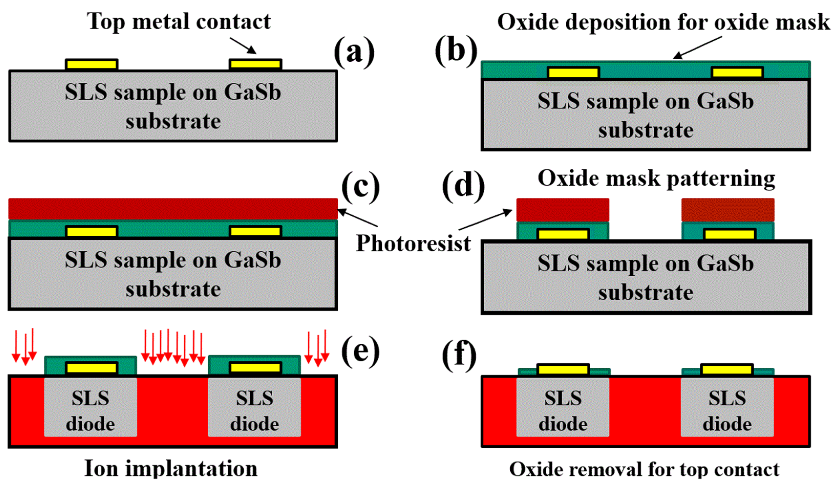
2. Materials and Methods
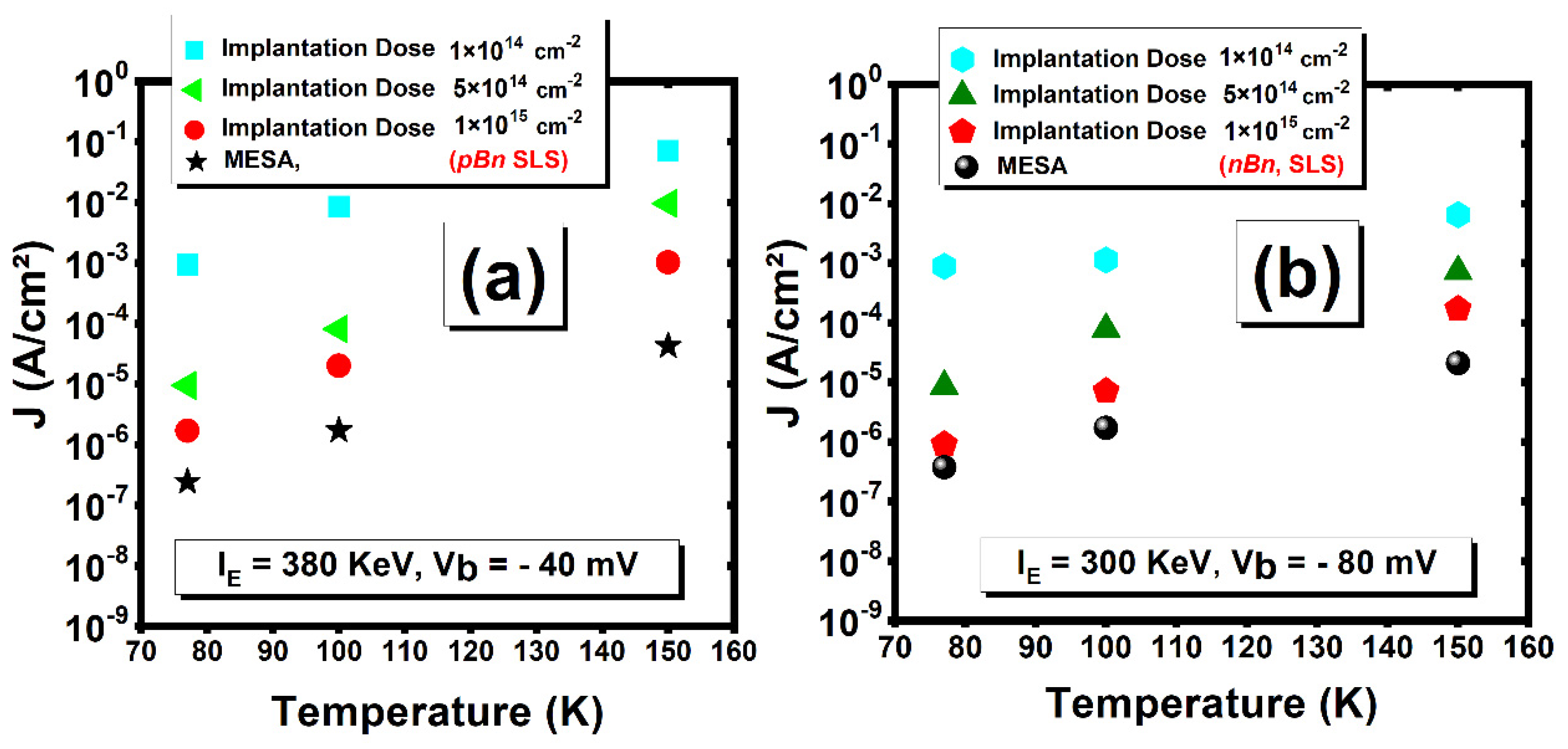
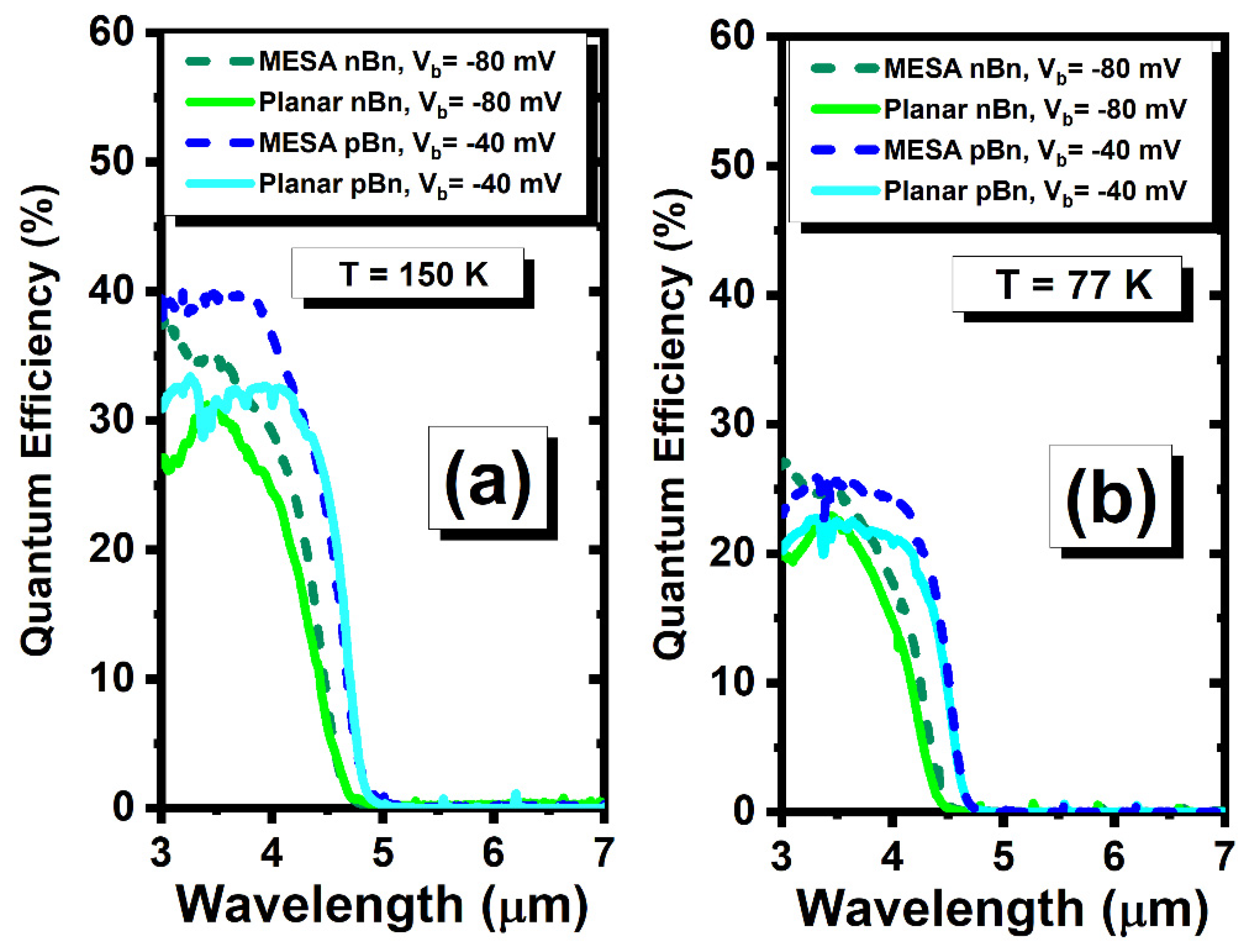
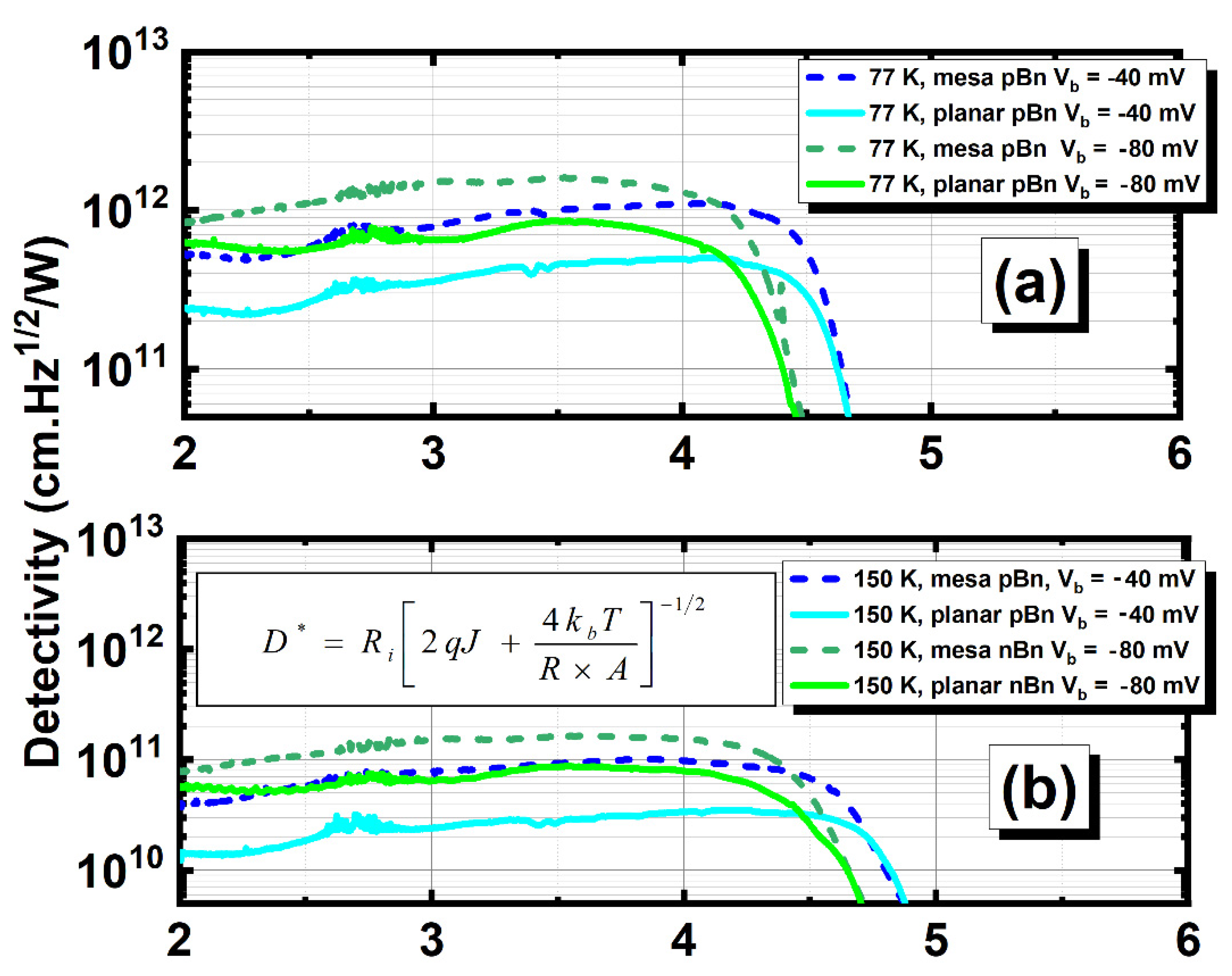
The material for this study was grown on a low Te-doped n-type GaSb (100) substrate, using a solid source molecular beam epitaxy (SS-MBE) reactor equipped with valved cracking sources for group-V and SUMO cells for group-III. The details about the growth for the nBn and pBn structures can be found elsewhere [19,28]. Both structures had the same barrier and absorption MWIR region (only the top contacts were different: p-type (for pBn) and n-type (for nBn)). The thickness of the top layer was adjusted accordingly to reflect the growth condition. This unipolar barrier structure design was chosen to allow a significant drop in electric field across the wide bandgap barrier to reduce generation–recombination currents. For the barrier, the SLS design was chosen to be AlAs0.5Sb0.5/InAs0.5Sb0.5, with a deep electron quantum well in the conduction band, which has been demonstrated to act as an effective wide-bandgap electron barrier for both nBn and pBn structures [28,29,30,31].
For the fabrication approach, a high quality 1-µm silicon-oxide layer was deposited as a hard mask to protect the diode area against the implantation. The oxide layer was deposited by plasma-enhanced chemical vapor deposition (PECVD), using a plasma of SiH4 and N2O gases. The thickness of the oxide layer was selected based on a simulation study using the stopping range of ions in matter (SRIM) software. Different steps of fabrication are schematically demonstrated in Figure 1. The first step was to deposit top metal contacts (a) on the as-grown surface, and then the silicon-oxide layer was deposited (b). This oxide layer was designed to act as a hard mask to protect the underneath SLS area, as well as the top metal contact. The oxide mask was then lithographically patterned on top of the wafers (c, d). The next step was to apply ion implantation on the isolation regions between diodes (e), whose top areas were covered by the hard mask. All samples were subjected to annealing for 15 s at 300 °C. Finally, the top metal contact was opened through the hard mask (f). The shape of the diodes was circular, with diameters ranging from 100 μm to 400 μm.
For the implantation process, the dose and acceleration energy required for effective isolation were studied and then optimized using the SRIM simulation tool. The penetration depth was a function of the implanted material nature and implantation energy, where the dose can signify the total number of implanted atoms. Although, finding an accurate ion-implantation profile would be hard to estimate, given the complexities of SLS material and the lack of enough empirical data on SLS material ion-implantation. Figure 2 illustrates an example of a simulation test result from the SRIM software for Si implantation distribution in different depths of an SLS pBn target, performed at two different implantation energies (IE), 100 keV (a) and 190 keV (b).
Based on the simulation result and the experimental consideration for pBn structure ion-implantation energies of 380, 190, and 100 KeV, and for the nBn structure the energies of 300, 190, and 100 KeV were chosen. For both cases and for each implantation energy, three ion-implantation doses of 1.0 × 10¹⁴, 5.0 × 10¹⁴, and 1.0 × 1015 cm−2 were used for a total of nine permutations. The implantation was performed with a tilt angle of 7° with no cooling (Innovion Corporation, San Jose, CA, USA). The purpose was to create n-type (silicon) and p-type (zinc) isolation regions on the top SLS layer. Both elements are heavy enough ions to generate damage on SLS structures with high carrier removal rates and destructibility to enforce effective isolation between adjacent diodes [23,32].
To make a meaningful comparison and create a baseline, standard mesa etched photodiodes were also processed from the same MBE grown. The fabrication approach for mesa-isolated diodes was reported elsewhere [33].

3. Results

Electrical testing was performed at different temperatures for all the SLS samples. The results showed that implantation energy and dose were the most critical parameters for the electrical performance analysis. The results showed that increasing the implantation energy can cause a drop in dark current for both nBn and pBn planar diodes. However, introducing high energy ions to the SLS structure can impose a great risk of damage-related increase in the dark current, such as hopping conduction effect [23,24]. Thus, the unlimited increase of dose or energy of implantation is not recommended and had to be optimized. Given that the implantation technique was used for diode formation, at higher implantation energies, each incident ion can reach deeper and cause more damage to the SLS structure, which in turn causes more isolation. Raising the dose can also provide similar impacts during implantation and creates effective isolation between adjacent diodes [23]. The best case is to optimize the dose and energy at the same time to achieve the most effective implantation approach. It was found that the implantation energy of 300 KeV for the nBn design and 380 KeV for the pBn design showed the lowest dark current values for each chosen implantation doses.
Figure 3a,b demonstrates a comparison of the dark current density versus the temperature of planar SLS diodes implanted with different implantation doses for pBn at −40 mV applied bias (Vb) (380 KeV implantation energy) (a) and nBn (Vb = −80 mV, 300 KeV implantation energy). The result led to the conclusion that the highest dose of 1 × 1015 cm−2 is the choice for the optimized condition for each case. Table 1 summarizes the optimized case of implantation for each device. Using the SRIM simulation for these optimized conditions, the estimated values for the depth of ion concentration peak and straggling inside the SLS material are given in Table 1 as well.
Figure 3 also presents an interesting comparison of the dark current density values for both the pBn and nBn planar and mesa-isolated devices. The results show that the dark current values for mesa-isolated SLS diodes were still lower compared to the planar diodes. This issue will be addressed shortly.
The dark current density values versus bias voltage at 77 K and 150 K for both optimized implantation conditions for the MWIR nBn and pBn planar devices are shown in Figure 4a,b, respectively. All the diodes had a 200-µm diameter circle shape. For the nBn device, the dark current density values at Vb = −80 mV at 77 K and 150 K were 1.23 × 10⁻⁶ A/cm2 and 1.42 × 10⁻⁴ A/cm2, respectively (Figure 4a). For the pBn device at the bias voltage of −40 mV, the dark current density values at 77 K and 150 K were 5.21 × 10⁻⁶ A/cm2 and 2.68 × 10⁻³ A/cm2, respectively (Figure 4b). In the inset of Figure 4, the dark current values for the optimized planar SLS photodetectors were compared with traditional mesa-isolated devices for the same size of diodes. As it can be seen, at the low range of temperature < 100 K, the values for the planar devices were in the range of 2–3 (for nBn) and 6–8 (for pBn) times higher compared to the mesa-isolated devices. The dark current performance was overall better for the planar nBn device compared to its pBn counterpart. The gap between the dark current value for planar and mesa-isolated SLS diodes was much worse at higher temperatures. At 150 K, the planar devices had more than one order of magnitude higher dark current, which must be addressed, especially for high operation temperature (HOT) aspects. This degradation of dark current at high temperatures for the planar SLS devices can be related to the nature of the defects created by the ion-implantation process and annealing treatment [23]. Further empirical and simulation studies of different aspects of ion-implantation for SLS material are strongly recommended. However, the outcome of this research would be a useful guideline for future work.
The comparison of the optical performance of both MWIR planar devices under optimized implantation at 77 K and 150 K is shown in Figure 5a,b. The calculated saturated QE values of both devices were also compared with the mesa-isolated devices. For the optical test, the top illumination approach was chosen with no anti–refection coatings, and a calibrated 1000 °C blackbody source and Fourier transform infrared (FTIR) spectrometer were used. For the nBn and pBn planar devices, saturated QE values were calculated at −80 mV and −40 mV bias voltage, respectively. The 50% cut-off wavelength for the nBn planar device at 77 K, was 4.10 µm, with a saturated peak responsivity (Ri) of 0.67 A/W at λ = 3.35 µm at a −80 mV applied bias. At 150 K, the saturated peak responsivity was 0.84 A/W at the same wavelength, with a 50% cut-off wavelength 4.40 µm. For the pBn device at 77 K and a −40 mV bias voltage, the 50% cut-off wavelength of the planar device was 4.40 µm with a peak responsivity of 0.76 A/W at 3.8 µm. At 150 K, the peak responsivity increased to 1.09 A/W. The corresponding saturated QE values at peak responsivity for both planar devices are summarized in Table 2, along with relevant QE values for mesa-isolated devices.
The specific detectivity (D*) values for both SLS structures have also been calculated for the optimized implantation parameters and compared with the mesa-etched device (Figure 6a,b). The D* values were calculated by the equation shown in Figure 6b at given applied bias for the peak responsivity provided earlier. Overall, for planar devices and similar to reticulated structures, a steady trend for the specific detectivity values were observed for the MWIR spectrum across a broad range of wavelengths, which is promising for different applications that require broad-band photodetection. This can offer a possible application for MWIR infrared imaging for phototransistors. The D* values are summarized in Table 3 for a 2π field of view (FOV) at 150 K and 77 K for a 200-diameter size of optimized implanted diodes and mesa-etched devices.
Both designs revealed similar performances, which was not far from expectations. There was a small gap in D* values between planar and mesa-isolated reference devices, which can be resolved and then surpassed by additional design and fabrication optimization. The trend of higher values for D* at lower temperatures for all devices (including reticulated and planar) came from the lower dark current values and higher resistance area product (R × A) values at lower temperatures for the photodetectors at given operational biases, which in turn caused high D* values (equation in inset of Figure 6b).

4. Discussion

For the nBn device, the QE values were lower but close enough to those for the mesa-isolated diodes. For the pBn design, on the other hand, the gap in QE values was higher compared to the mesa-isolated devices. The reason for the effect is still unknown, but there was a speculation that it might be associated with the optical contribution of the sloped mesa sidewalls (mirror effect) to increase the QE a bit. There was also a difference in QE values at 77 K and 150 K for each device, which is related to the limitation of n-type absorbers of Ga-free (InAs/InAsSb) SLS material, due to lower hole mobility values at lower temperatures.
It has been reported that Ga free n-type absorbers deliver lower QE in general, due to shorter hole diffusion lengths and modest absorption coefficients [12,34,35]. The lower QE values at lower temperatures is also suspected to be electrically related to recombination occurring in the ion-implanted region at the periphery of the device at different temperatures. This hypothesis should be confirmed by a more detailed study on the temperature dependence of dark current.
The uniformity level of the optical performances of the SLS planar devices was evaluated for optimized implantation parameters to make sure of the proper diode isolation by the implantation technique. To do so, the optical test was performed on different diode sizes at different temperatures, and it was confirmed that the QE values did not change across the different range of diode sizes. This is promising for focal plane array applications, which entails the scalability of the suggested method. It is worth noting that lower ion implantation energy can cause partial isolation, meaning that the energy is not strong enough to penetrate deeply into the substrate to pass the barrier (i.e., not reaching to absorption region) and generate isolated diodes. This means that the signal could come from the large area of the active region under the surface (much larger than the actual size of the diode), contributing to the responsivity, which causes inaccurate and large optical responses (e.g., QE > 100%). To evaluate this explanation, further simulations and empirical data are needed, which can be considered for the future direction of the study.

5. Conclusions

A novel approach based on the ion-implantation was implemented for pixel diode isolation for MWIR SLS-based heterostructure photodetectors. The different steps in the simulation and performance of ion-implantation were addressed, and the performance of the planar nBn and pBn heterostructure InAs/InAsSb SLS photodetectors were compared with each other and with reference mesa-isolated diodes. The planar fabrication method suggests that, instead of using ion-implantation for diffusion or doping the substrate, it should be used to perform ion-bombardment on substrates to selectively form highly-resistive regions and isolate the pixels from each other. Both devices revealed similar performances, not very far from their mesa-isolated counterpart devices. Overall, the method may have merits to pursue with promising results. There are some relevant concerns about electrical or optical cross talk between the pixels, which might drastically affect the modulation transfer function (MTF) performance of FPAs fabricated by the method, which has to be investigated in further studies. Another appealing subject of the study is to focus on scaling the pixel size down to the level of present interest in FPA applications (around 10 µm). Changing the design of the devices to suppress the dark current, such as a different form of heterojunction structure with multiple or higher barriers, or using thinner barrier/top contact to allow more effective diode isolation can be another consideration. By optimizing and developing the structure design of the SLS device and ion-implanting process, it is possible to surpass the mesa-isolated device performance for SLS planar devices.

Funding

The research that was reviewed in this paper was performed at Northwestern University and NOUR, LLC. This work was supported through SBIR program by the US Army under Contract No. W909MY-19-P-0027.

Institutional Review Board Statement

Not applicable.

Informed Consent Statement

Not applicable.

Data Availability Statement

The data that support the findings of this study are available from the corresponding author upon reasonable request.

Acknowledgments

The author would like to acknowledge great help and support from Ryan McClintock and Donghai Wu. The author is also grateful for the support from Manijeh Razeghi, the director of the Center for Quantum Devices. The author is now with Leonardo DRS.

Conflicts of Interest

The author declares no conflict of interest.

References

  1. Rogalski, A.; Martyniuk, P.; Kopytko, M. Type-II superlattice photodetectors versus HgCdTe photodiodes. Prog. Quantum Electron. 2019, 68, 100228. [Google Scholar] [CrossRef]
  2. Razeghi, M.; Haddadi, A.; Dehzangi, A.; Chevallier, R.; Yang, T. Recent advances in InAs/InAs1-xSbx/AlAs1-xSbx gap-engineered type-II superlattice-based photodetectors. In Proceedings of the Infrared Technology and Applications XLIII, Anaheim, CA, USA, 9–13 April 2017; SPIE: Bellingham, WA, USA, 2017; Volume 10177, pp. 19–29. [Google Scholar]
  3. Piotrowski, J.; Piotrowski, A. Room temperature IR photodetectors. Mercury Cadmium Telluride Growth Prop. Appl. 2010, 513–537. [Google Scholar] [CrossRef]
  4. Kinch, M.A. Fundamentals of Infrared Detector Materials; SPIE: Bellingham, WA, USA, 2007. [Google Scholar]
  5. Blanks, D.K.; Beck, J.D.; Kinch, M.A.; Colombo, L. Band-to-band tunnel processes in HgCdTe: Comparison of experimental and theoretical studies. J. Vac. Sci. Technol. A 1988, 6, 2790–2794. [Google Scholar] [CrossRef]
  6. Dehzangi, A.; Haddadi, A.; Adhikary, S.; Razeghi, M. Impact of scaling base thickness on the performance of heterojunction phototransistors. Nanotechnology 2017, 28, 10LT01. [Google Scholar] [CrossRef]
  7. Dehzangi, A.; McClintock, R.; Wu, D.; Li, J.; Johnson, S.M.; Dial, E.; Razeghi, M. High speed antimony-based superlattice photodetectors transferred on sapphire. Appl. Phys. Express 2019, 12, 116502. [Google Scholar] [CrossRef]
  8. Hoang, A.M.; Dehzangi, A.; Adhikary, S.; Razeghi, M. High performance bias-selectable three-color Short-wave/Mid-wave/Long-wave Infrared Photodetectors based on Type-II InAs/GaSb/AlSb superlattices. Sci. Rep. 2016, 6, 24144. [Google Scholar] [CrossRef] [Green Version]
  9. Nguyen, B.-M.; Hoffman, D.; Delaunay, P.-Y.; Huang, E.K.-W.; Razeghi, M.; Pellegrino, J. Band edge tunability of M-structure for heterojunction design in Sb based type II superlattice photodiodes. Appl. Phys. Lett. 2008, 93, 163502. [Google Scholar] [CrossRef]
  10. Binh-Minh, N.; Guanxi, C.; Minh-Anh, H.; Razeghi, M. Growth and Characterization of Long-Wavelength Infrared Type-II Superlattice Photodiodes on a 3-in GaSb Wafer, Quantum Electronics. IEEE J. Quantum Electron. 2011, 47, 686–690. [Google Scholar] [CrossRef]
  11. Zegrya, G.G.; Andreev, A.D. Mechanism of suppression of Auger recombination processes in type-II heterostructures. Appl. Phys. Lett. 1995, 67, 2681–2683. [Google Scholar] [CrossRef]
  12. Ting, D.Z.; Soibel, A.; Khoshakhlagh, A.; Keo, S.A.; Rafol, B.; Fisher, A.M.; Pepper, B.J.; Luong, E.M.; Hill, C.J.; Gunapala, S.D. Advances in III-V semiconductor infrared absorbers and detectors. Infrared Phys. Technol. 2019, 97, 210–216. [Google Scholar] [CrossRef]
  13. Ting, D.Z.-Y.; Hill, C.J.; Soibel, A.; Keo, S.A.; Mumolo, J.M.; Nguyen, J.; Gunapala, S.D. A high-performance long wavelength superlattice complementary barrier infrared detector. Appl. Phys. Lett. 2009, 95, 023508. [Google Scholar] [CrossRef]
  14. Arias, J.M.; Pasko, J.G.; Zandian, M.; Shin, S.H.; Williams, G.M.; Bubulac, L.O.; DeWames, R.E.; Tennant, W.E. Planar p-on-n HgCdTe heterostructure photovoltaic detectors. Appl. Phys. Lett. 1993, 62, 976–978. [Google Scholar] [CrossRef]
  15. Musca, C.A.; Antoszewski, J.; Dell, J.M.; Faraone, L.; Terterian, S. Planar p-on-n HgCdTe heterojunction mid-wavelength infrared photodiodes formed using plasma-induced junction isolation. J. Electron. Mater. 2003, 32, 622–626. [Google Scholar] [CrossRef]
  16. Chang, S.-H.; Fang, Y.-K.; Ting, S.-F.; Chen, S.-F.; Lin, C.-Y.; Wu, C.-Y. Ultra high performance planar InGaAs PIN photodiodes for high speed optical fiber communication. Sens. Actuators A Phys. 2007, 133, 9–12. [Google Scholar] [CrossRef]
  17. Arias, J.; Pasko, J.G.; Zandian, M.; Shin, S.H.; Williams, G.M.; Bubulac, L.O.; De Wames, R.E.; Tennant, W.E. MBE HgCdTe heterostructure p-on-n planar infrared photodiodes. J. Electron. Mater. 1993, 22, 1049–1053. [Google Scholar] [CrossRef]
  18. Kinch, M. HDVIP FPA Technology at DRS Infrared Technologies (Aerospace/Defense Sensing, Simulation, and Controls); SPIE: Bellingham, WA, USA, 2001. [Google Scholar]
  19. Dehzangi, A.; Wu, D.; McClintock, R.; Li, J.; Razeghi, M. Planar nBn type-II superlattice mid-wavelength infrared photodetectors using zinc ion-implantation. Appl. Phys. Lett. 2020, 116, 221103. [Google Scholar] [CrossRef]
  20. Dehzangi, A.; Wu, D.; McClintock, R.; Li, J.; Jaud, A.; Razeghi, M. Demonstration of Planar Type-II Superlattice-Based Photodetectors Using Silicon Ion-Implantation. Photonics 2020, 7, 68. [Google Scholar] [CrossRef]
  21. Wu, D.; Dehzangi, A.; Li, J.; Razeghi, M. High performance Zn-diffused planar mid-wavelength infrared type-II InAs/InAs1−xSbx superlattice photodetector by MOCVD. Appl. Phys. Lett. 2020, 116, 161108. [Google Scholar] [CrossRef] [Green Version]
  22. Dehzangi, A. Planar strained layer superlattice infrared photodetector using ion implantation. In Proceedings of the Image Sensing Technologies: Materials, Devices, Systems, and Applications IX, Orlando, FL, USA, 3 April–13 June 2022; SPIE: Bellingham, WA, USA, 2022; Volume 12091, pp. 9–15. [Google Scholar]
  23. Pearton, S.J. Ion implantation for isolation of III–V semiconductors. Mater. Sci. Rep. 1990, 4, 313–363. [Google Scholar] [CrossRef]
  24. Eisen, F.H. Ion implantation in III–V compounds. Radiat. Eff. 1980, 47, 99–115. [Google Scholar] [CrossRef]
  25. Donnelly, J.P. The electrical characteristics of ion implanted compound semiconductors. Nucl. Instrum. Methods 1981, 182–183, 553–571. [Google Scholar] [CrossRef]
  26. Steenbergen, E.H.; Connelly, B.C.; Metcalfe, G.D.; Shen, H.; Wraback, M.; Lubyshev, D.; Qiu, Y.; Fastenau, J.M.; Liu, A.W.K.; Elhamri, S.; et al. Significantly improved minority carrier lifetime observed in a long-wavelength infrared III–V type-II superlattice comprised of InAs/InAsSb. Appl. Phys. Lett. 2011, 99, 251110. [Google Scholar] [CrossRef]
  27. Razeghi, M.; Haddadi, A.; Hoang, A.M.; Chevallier, R.; Adhikary, S.; Dehzangi, A. InAs/InAs1−xSbx type-II superlattices for high performance long wavelength infrared detection. In Proceedings of the Infrared Technology and Applications XLII, Baltimore, MD, USA, 18–21 April 2016; Volume 9819, p. 981909. [Google Scholar]
  28. Wu, D.; Li, J.; Dehzangi, A.; Razeghi, M. Mid-wavelength infrared high operating temperature pBn photodetectors based on type-II InAs/InAsSb superlattice. AIP Adv. 2020, 10, 025018. [Google Scholar] [CrossRef] [Green Version]
  29. Soibel, A.; Ting, D.Z.; Rafol, S.B.; Fisher, A.M.; Keo, S.A.; Khoshakhlagh, A.; Gunapala, S.D. Mid-wavelength infrared InAsSb/InAs nBn detectors and FPAs with very low dark current density. Appl. Phys. Lett. 2019, 114, 161103. [Google Scholar] [CrossRef]
  30. Haddadi, A.; Dehzangi, A.; Chevallier, R.; Adhikary, S.; Razeghi, M. Bias–selectable nBn dual–band long–/very long–wavelength infrared photodetectors based on InAs/InAs1−xSbx/AlAs1−xSbx type–II superlattices. Sci. Rep. 2017, 7, 3379. [Google Scholar] [CrossRef] [Green Version]
  31. Wu, D.; Dehzangi, A.; Razeghi, M. Demonstration of mid-wavelength infrared nBn photodetectors based on type-II InAs/InAs1−xSbx superlattice grown by metal-organic chemical vapor deposition. Appl. Phys. Lett. 2019, 115, 061102. [Google Scholar] [CrossRef]
  32. Asano, T.; Atanassov, R.D.; Ishiwara, H.; Furukawa, S. Formation of Thick, Thermally-Stable High-Resistivity-Layers in GaAs by Oxygen Ion Implantation. Jpn. J. Appl. Phys. 1981, 20, 901–907. [Google Scholar] [CrossRef]
  33. Dehzangi, A.; McClintock, R.; Haddadi, A.; Wu, D.; Chevallier, R.; Razeghi, M. Type–II superlattices base visible/extended short–wavelength infrared photodetectors with a bandstructure–engineered photo–generated carrier extractor. Sci. Rep. 2019, 9, 5003. [Google Scholar] [CrossRef] [Green Version]
  34. Matsubara, M.; Kyrtsos, A.; Bellotti, E. Phase diagrams and critical temperatures for coherent and incoherent mixtures of InAs1−xSbx alloys using first-principles calculations. J. Appl. Phys. 2022, 131, 215102. [Google Scholar] [CrossRef]
  35. Ting, D.Z.; Fisher, A.M.; Pepper, B.J.; Hill, C.J.; Keo, S.A.; Khoshakhlagh, A.; Soibel, A.; Rafol, B.; Maruyama, Y.; Gunapala, S.D.; et al. Progress in InAs/InAsSb superlattice barrier infrared detectors. In Proceedings of the Infrared Technology and Applications XLVIII, Orlando, FL, USA, 3 April–13 June 2022; Volume 12107, pp. 167–175. [Google Scholar]
Figure 1. Schematic diagram of the process flow for the fabrication planar SLS photodetectors: (a) top metal contact, (b) deposition of the oxide mask, (c,d) patterning via photolithography, (e) implantation for diode isolation, and (f) top metal contact window opening.
Applsci 12 06114 g001
Figure 2. Simulation results performed using SRIM software for distribution of the Si ions in different depths of the target for various implantation energies: (a) IE = 100 keV, (b) IE = 190 keV.
Applsci 12 06114 g002
Figure 3. (a) Dark current values versus temperature for the planar MWIR SLS diodes: (a) pBn (Vb = −40 mV, 380 KeV implantation dose) and (b) nBn (Vb = −80 mV, 300 KeV implantation dose) fabricated with different implantation doses. All diodes were circular with a 200-µm diameter.
Applsci 12 06114 g003
Figure 4. (a) Dark current density vs. applied bias voltage of the optimized ion-implantation condition at 77K and 150 K for MWIR nBn (a) and pBn (b) planar devices. The inset of each part compares the dark current density values for planar and mesa-etched photodetectors at 77, 100, and 150 K. All diodes were circular with a 200-µm diameter.
Applsci 12 06114 g004
Figure 5. Saturated 77 (a) and 150 K (b) QE spectra measured for planar and mesa-etched MWIR SLS photodetectors (diode with 200 µm diameter).
Applsci 12 06114 g005
Figure 6. D* spectrum at (a) 77 K and (b) 150 K for planar and mesa-isolated MWIR SLS devices (diodes with 200 µm diameter). The D* values were calculated using the equation in the inset, where kb is the Boltzmann constant, T is the operating temperature, J is the dark current, and R × A is the resistance area product.
Applsci 12 06114 g006
Table 1. Optimized implantation parameters for the pBn and nBn designs.
DesignImplantation
Energy
Implantation
Dose
Depth of Ion Concentration PeakStraggling
pBn300 KeV1 × 1015 cm−2900 nm100 nm
nBn380 KeV1 × 1015 cm−21000 nm115 nm
Table 2. Comparison of the QE values at peak responsivity for planar and mesa-isolated SLS devices at 77 and 150 K. (Vb = −40 mV for pBn and Vb = −80 mV for nBn).
DesignFabrication ApproachQE @ 150 KQE @ 77 K
nBn
λ = 3.35 µm
Mesa36.4%25.0%
Planar31.5%23.5%
pBn
λ = 3.80 µm
Mesa39.2%24.4%
Planar32.6%21.5%
Table 3. Comparison of the D* values for planar and mesa-etched SLS devices at 77 and 150 K. (Vb = −40 mV for pBn and Vb = −80 mV for nBn).
Design Fabrication ApproachD* @ 150 K
cm⸱Hz1/2/W
D* @ 77 K
cm⸱Hz1/2/W
nBn
λ = 3.35 µm
Mesa1.86 × 1011 1.52 × 10¹²
Planar8.54 × 10109.12 × 1011
pBn
λ = 3.80 µm
Mesa3.37 × 10101.52 × 1012
Planar4.95 × 10111.10 × 1012
Publisher’s Note: MDPI stays neutral with regard to jurisdictional claims in published maps and institutional affiliations.

