Article

Design of an Interface Layer Using CPW between an Array Antenna and TRM in X-Band Radar Systems to Minimize Leakage Fields and Improve Transmission Characteristics

1
Department of Electronic and Electrical Engineering, Hongik University, Seoul 04066, Korea
2
LIG Nex1 Microwave and Antenna R&D, Yongin 16911, Korea
*
Author to whom correspondence should be addressed.
Appl. Sci. 2022, 12(17), 8514; https://doi.org/10.3390/app12178514
Submission received: 23 July 2022 / Revised: 24 August 2022 / Accepted: 24 August 2022 / Published: 25 August 2022

Abstract

:
In this paper, we propose an interface layer using the coplanar waveguide (CPW) between an array antenna and transmitting receiver modules (TRMs) for X-band military ship radar systems. To improve transmission characteristics, the interface layer with the CPW has three transition parts: Transition part A is between the sub miniature push-on (SMP) connector and the interface layer. Transition part B is the CPW in which the thickness gradually increases. Transition part C is for connecting the interface layer and the antenna. The measured reflection and transmission coefficients of the fabricated interface layer are −22.4 dB and −0.82 dB, respectively. To verify the proposed interface layer, we then apply the layer to a 2 × 2 X-band array antenna and measure the array antenna characteristics, such as reflection coefficients, array antenna gain, and half-power beam widths (HPBWs). The measured reflection coefficient is under −10 dB from 8.6 GHz to 10.2 GHz, and the bore-sight array gain of the 2 × 2 array antenna is 10.5 dBi at 9.5 GHz. In addition, the measured HPBWs under the same conditions are 47.8° and 39.1° in the zx- and zy-planes, respectively. The results demonstrate that the proposed interface layer using the CPW is suitable for X-band radar systems.

1. Introduction

Recently, with the gradual development of military ship radar systems, the demand for improved design technologies for X-band array antennas has been increasing for target search and tracking, maritime traffic monitoring, and maritime navigation [1,2,3]. In such radar systems, various antenna types, such as horn antennas [4,5], conical antennas [6,7], and Vivaldi antennas [8,9,10,11], have been implemented as X-band radar elements. However, when such antenna elements are mounted on ship radars, there is a critical disadvantage in that they are structurally unstable due to their bulky size and heavy weight. To resolve these problems, patch array antennas are typically used in X-band marine radar systems due to their light weight, ease of manufacturing, and low profile [12,13,14,15]. Since an X-band radar system must be capable of electric beam steering, a patch array antenna should be connected to transmitting receiver modules (TRMs) [16,17,18]. To stably connect the antenna and the TRMs, interface layers are often employed between the antenna and the TRM using various transmission lines, such as coplanar waveguides (CPWs) [19], microstrip lines [20], and strip lines [21]. Although some research has been conducted to develop interface layers with improved reflection and transmission characteristics, there is not enough in-depth consideration of the performance when the interface layer is mounted on the array antennas of actual radar systems.
In this paper, we propose an interface layer using a CPW between an array antenna and TRMs for X-band ship radar systems. To improve transmission characteristics, the interface layer with the CPW consists of three transition parts: Transition part A is applied between the sub miniature push-on (SMP) connector and the interface layer. Transition part B is the CPW in which the thickness gradually increases between the thin and thick CPWs in the interface layer. Transition part C is implemented between the interface layer and the antenna. Through the optimal design of these transition parts, the transmission characteristics of the interface layer are improved, while the leakage fields that cause power loss are minimized. This can achieve enhanced array antenna performance when the interface layer is mounted on actual radar systems. Herein, the target frequency band is determined from 9 GHz to 10 GHz, which is typically used in actual X-band radar systems [22,23]. For performance verification, the proposed interface layer is fabricated, and the reflection and transmission coefficients are measured in a full anechoic chamber. Moreover, to examine the interface layer’s performance when it is mounted on actual radar systems, a fabricated 2 × 2 X-band array antenna is connected to the proposed interface layer. Array characteristics including the interface layer, such as the reflection coefficients of array elements and the array beam patterns are measured and compared with simulation results. The results demonstrate that the proposed interface layer using the CPW is suitable for X-band marine radar systems.

2. Proposed Interface Layer Using a CPW

2.1. Geometry of the Interface Layer Using the CPW

Figure 1 presents the geometry of the interface layer using the CPW considering the connection part between the antenna and TRM in X-band radar systems. To enhance the transmission characteristics and minimize the leakage fields of the CPW, the proposed interface layer consists of three transition parts: A, B, and C. Transition part A is located between the SMP connector and the CPW line of the interface layer. The SMP is a surface-mounted connector, and it is generally recommended with this connector to use a CPW without ground [24]. However, to enhance the transmission characteristics with minimum leakage of electric fields, vias should be densely inserted into the ground plane around the CPW. X-band radar systems typically use a small connector due to the narrow array distances of the antenna elements. Thus, the CPW line mounted on the SMP connector has a thin width of w1 and a gap of g1, as shown in Figure 1b. In contrast, the CPW line near the SMP connector has a greater width of w2 and a gap of g2 to prevent dropout of the inner metallic line when the feed-pin is connected to the CPW line using solder. Transition part B is the CPW, the thickness of which gradually increases between the thin and thick CPWs in the interface layer. The width of this transition line with a length of d1 is gradually varied from w1 to w2 to obtain suitable impedance-matching characteristics. Finally, transition part C is implemented between the ground of the CPW and the feed-pin, as shown in Figure 1c. The transition part C comprises the feed-pin radius (rf) and the radius of the perforated part of the ground plane (rd). The transmission characteristics of the interface layer can be further enhanced by adjusting the ratio of rf to rd. The proposed interface layer using the CPW uses an FR-4 substrate (εr = 4.4, tan δ = 0.027) with a thickness of h1, and it is designed using a FEKO full electromagnetic simulator [25]. The detailed design parameters of the proposed interface layer using the CPW are listed in Table 1.

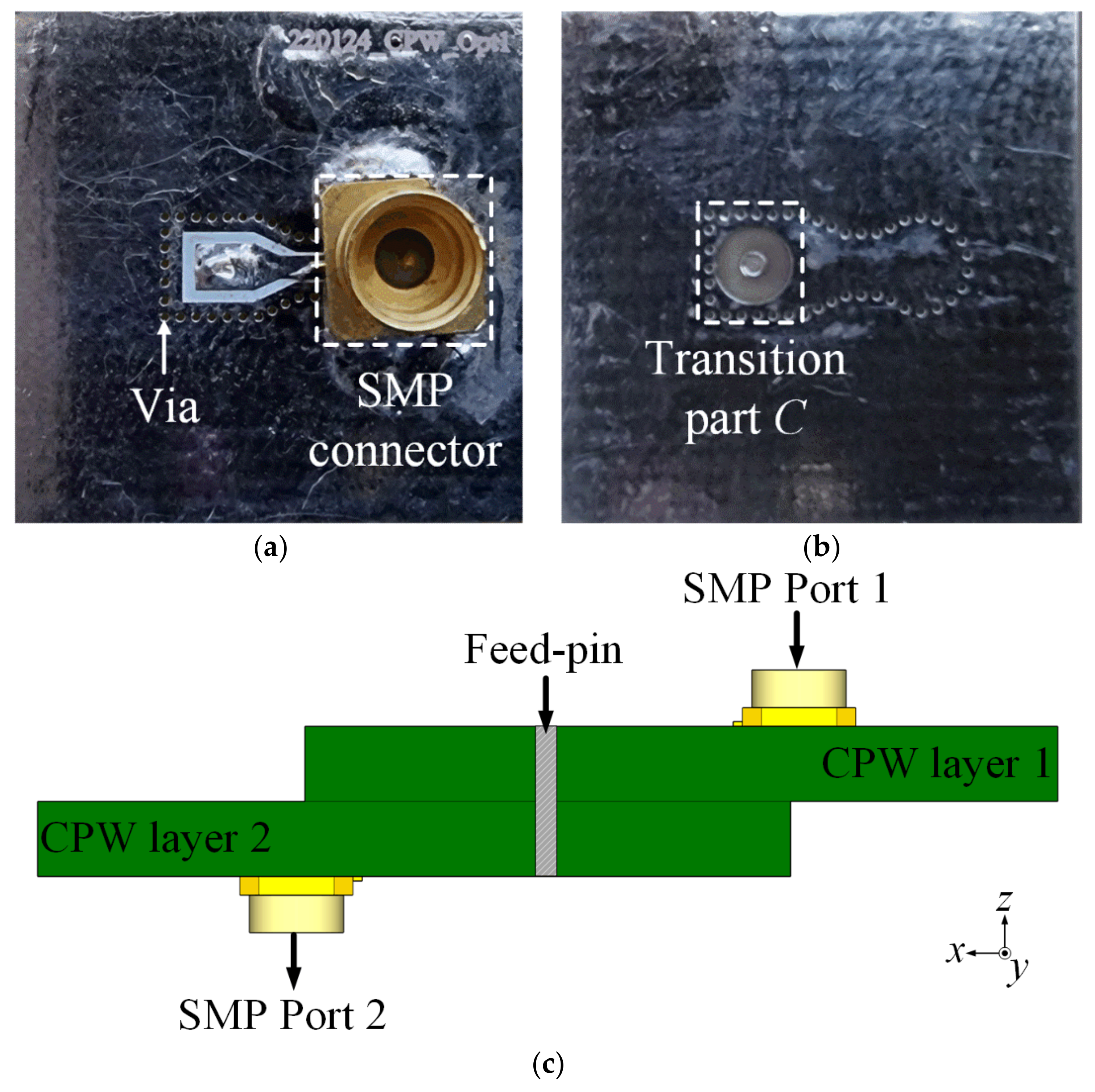
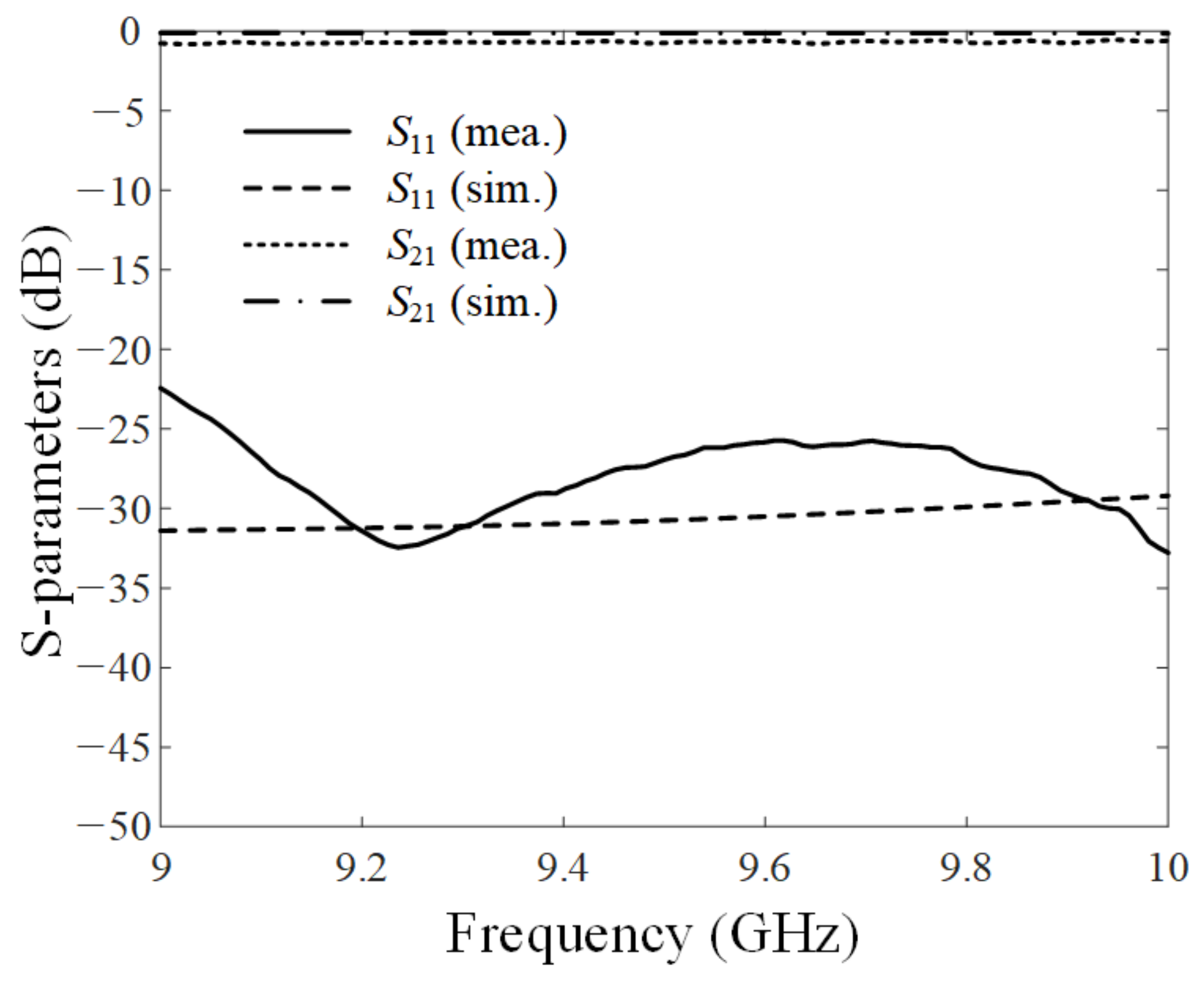
2.2. Fabrication and Measurement

Figure 2a,b present photographs of the fabricated interface layer. The fabricated interface layer using the CPW has dense vias around the CPW line. The SMP connector and feed-pin are combined with the CPW of the interface layer by soldering. To measure its transmission coefficients, the proposed interface layer is extended to a back-to-back configuration, which allows for investigation of radar performance degradation caused by the interface layer, as shown in Figure 2c. Figure 2d illustrates a photograph of the fabricated back-to-back configuration. In this configuration, the bottoms of the CPWs face each other, and the feed-pin penetrates the two CPW layers. To verify its feasibility, the fabricated interface layer in the back-to-back configuration is measured in a full anechoic chamber. Figure 3 represents the measured and simulated reflection (S11) and transmission coefficients (S21) of the proposed interface layer in the back-to-back configuration. The measured (solid line) and simulated (dashed line) reflection coefficients are below −22.4 dB and −29.2 dB, respectively, in the operating frequency. In addition, the transmission coefficients for the measured results exceed −0.82 dB (dotted line), and for the simulated results exceed −0.14 dB (dashed–dotted line). The interface layer characteristics, such as reflection coefficient, target frequency, and interface layer size, are listed in Table 2 to compare them with previous studies. The proposed interface layer has good reflection characteristics and a small size in our target frequency band from 9 GHz to 10 GHz. These results demonstrate that the performance of the proposed interface layer using the CPW is suitable for X-band radar applications.
Table 2. Comparisons of the interface layer characteristics.
ResearchReflection
Coefficient
Target
Frequency
Size (mm)
[16]−20 dB8–12 GHz13 × 16 × -
[19]-8.5–11 GHz14 × 14 × 6.1
[20]−13.3 dB8.5–10.5 GHz20 × 20 × 3.7
[21]−20.8 dB8.8–10.4 GHz20 × 20 × 2.6
Proposed interface layer−26.9 dB9–10 GHz17 × 17 × 0.8

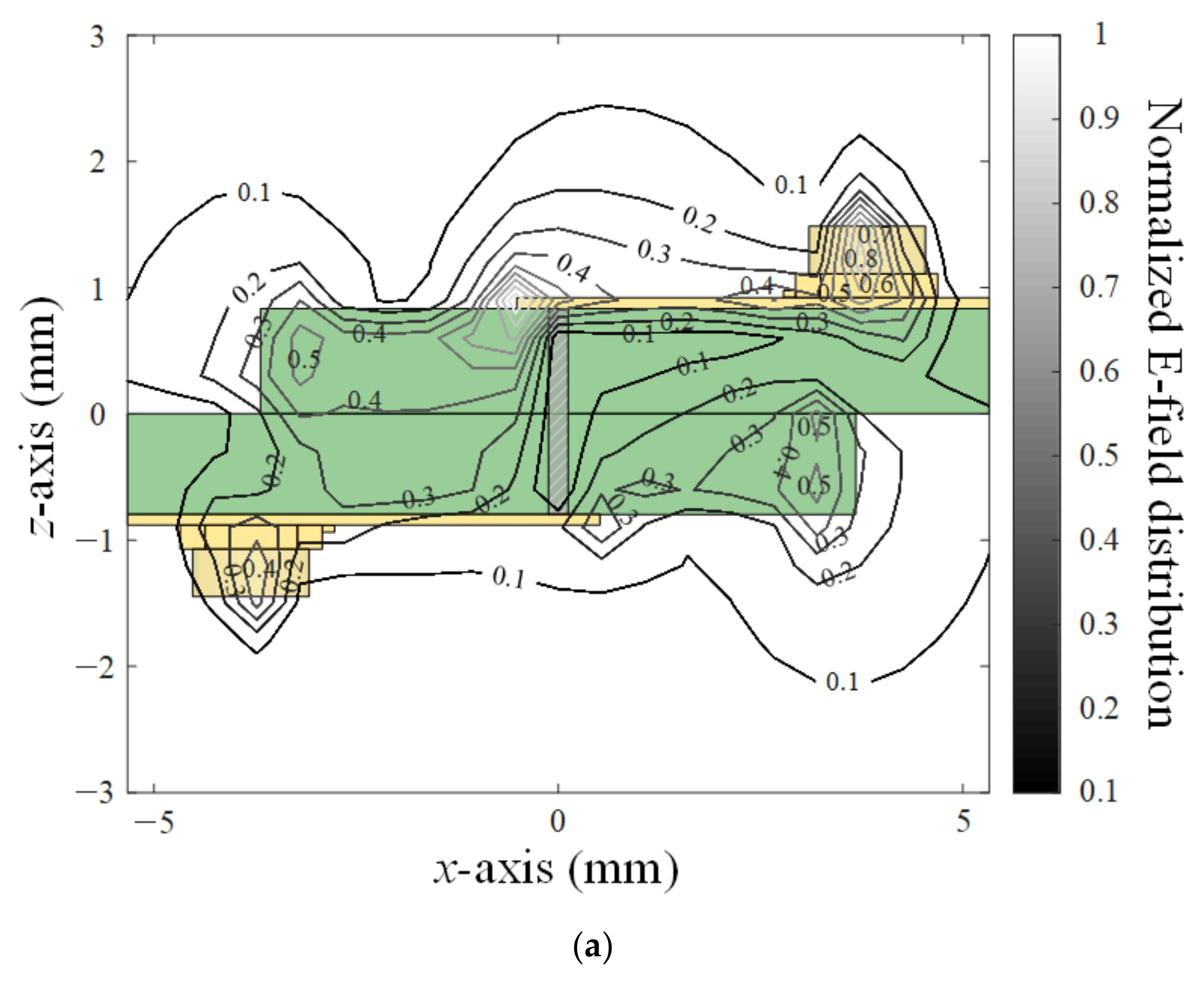
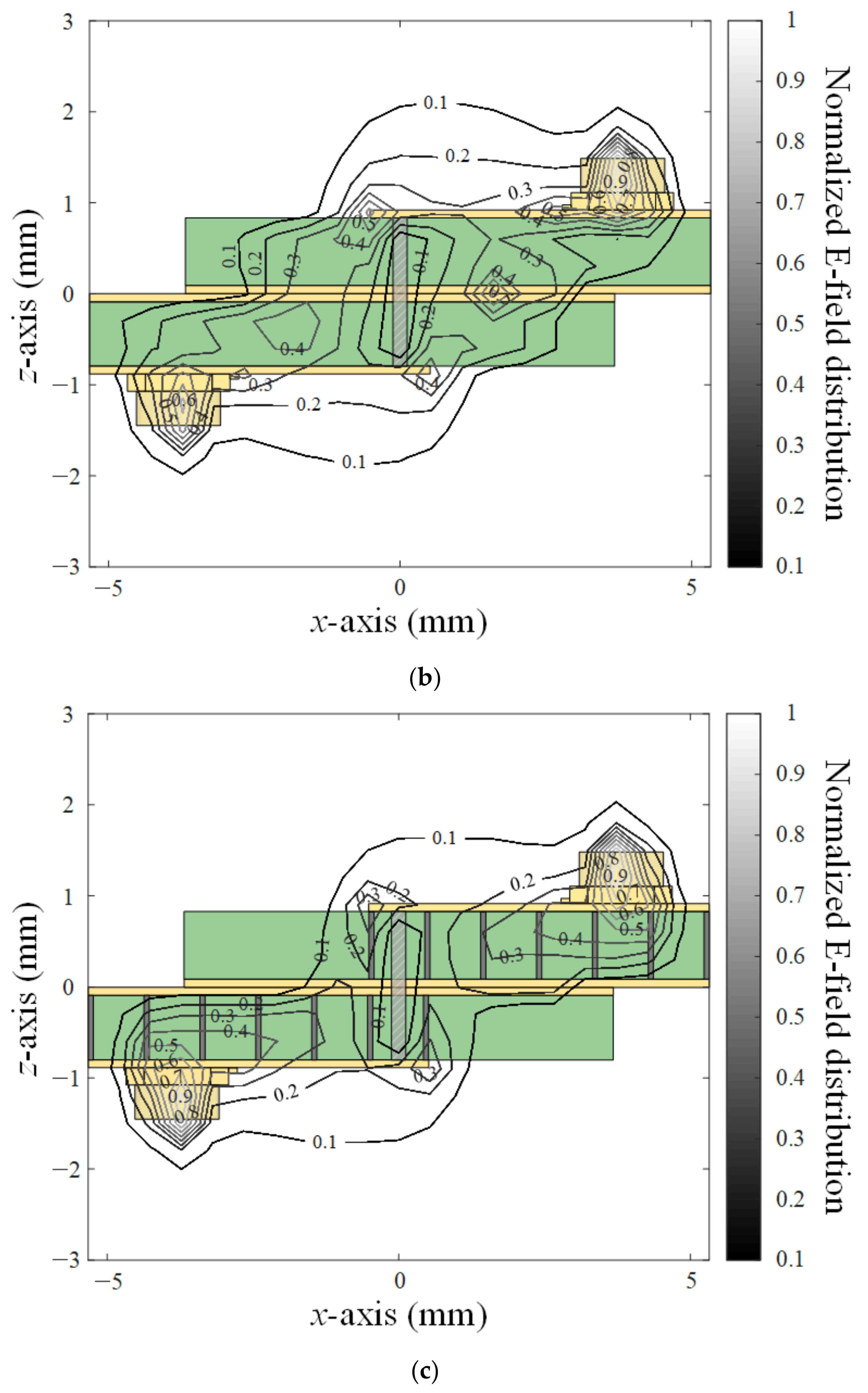
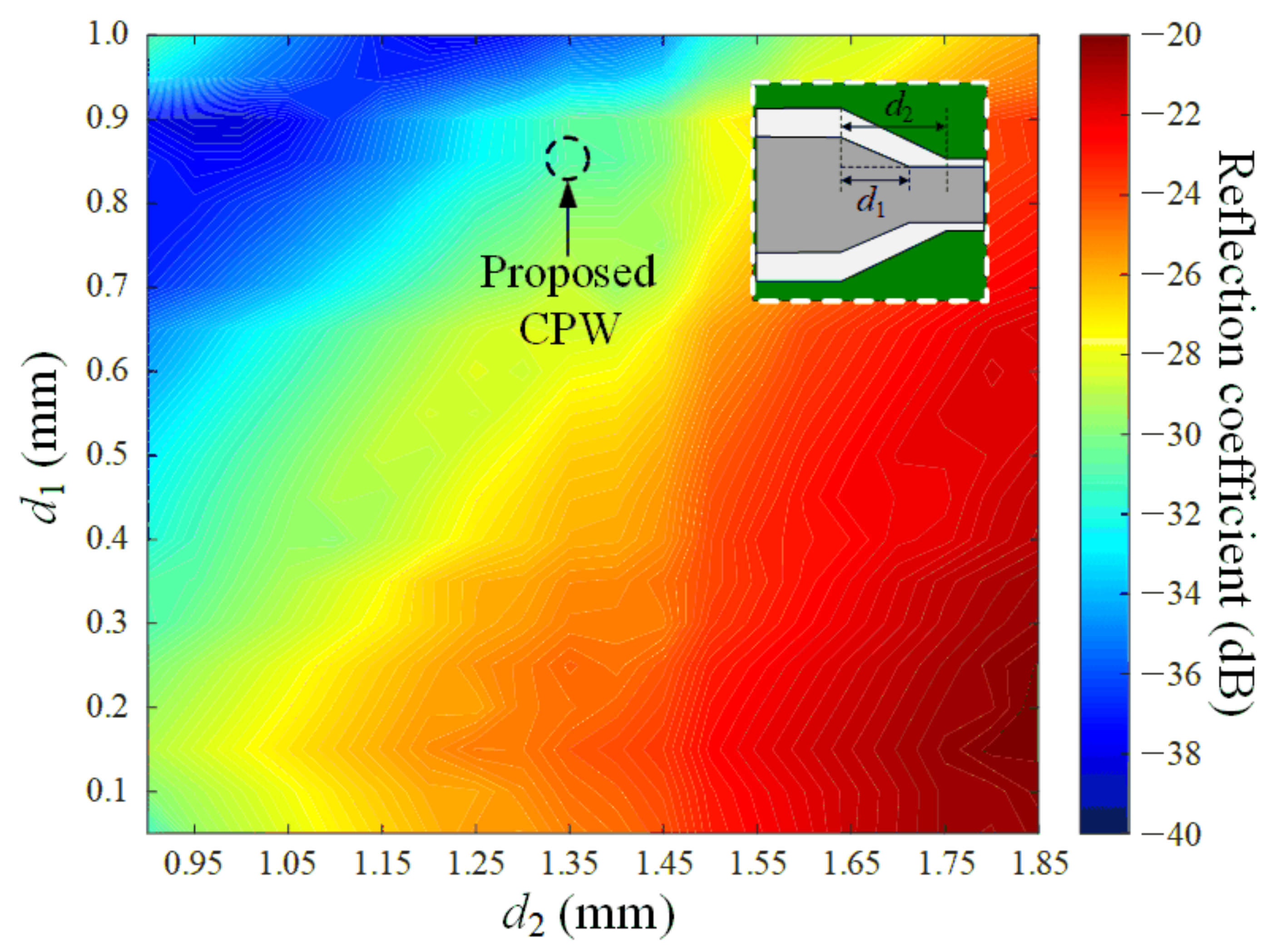
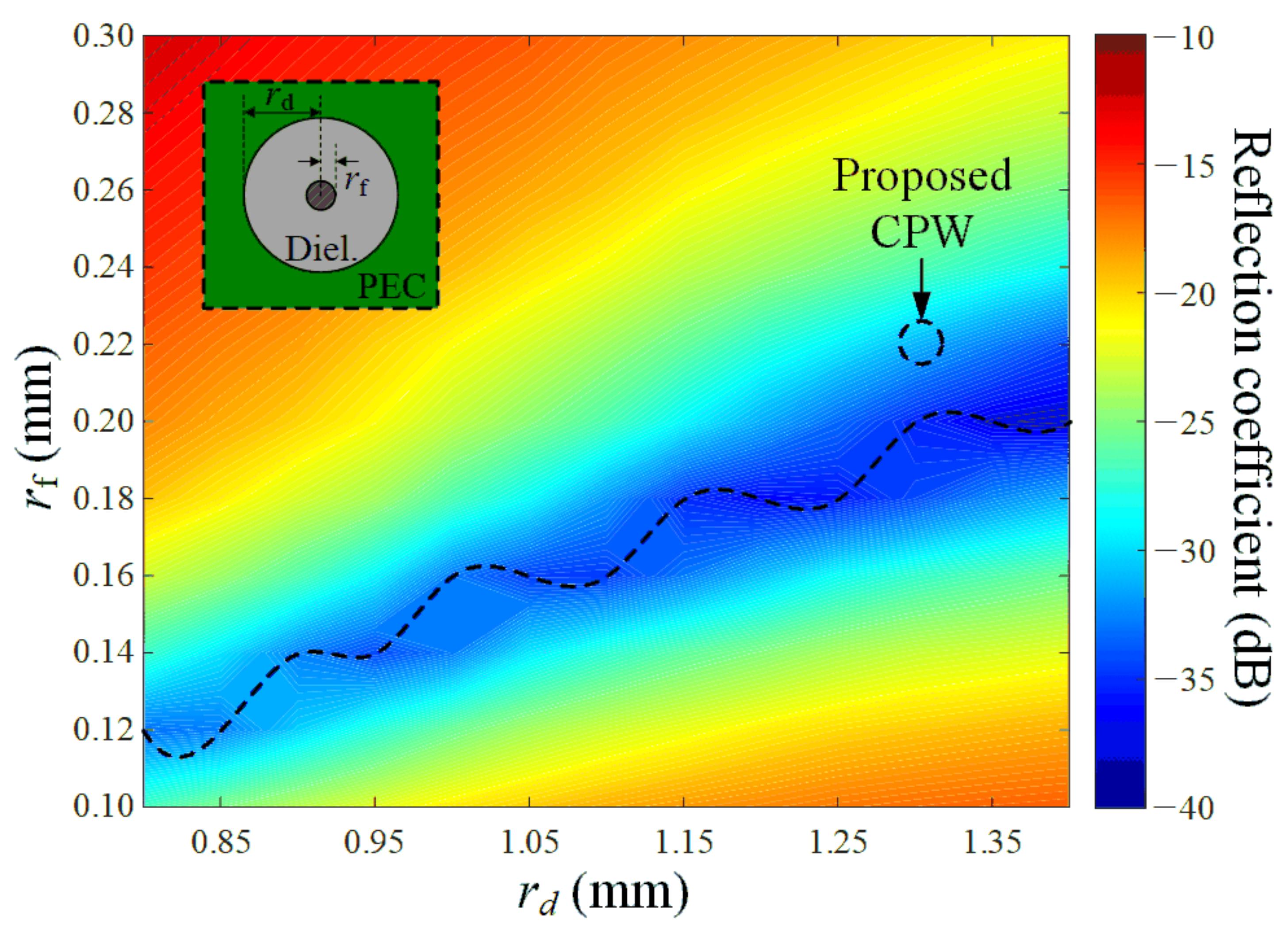
2.3. Analysis of the Transitions of the Proposed Interface Layer

Figure 4 shows the normalized E-field distributions according to the configurations in transition part A. The E-field distributions were investigated on the zx-plane (y = 0 mm) at an observation frequency of 9.5 GHz. To analyze the influence of the configurations, we investigated the normalized E-field to observe the leakage E-field in the ranges of 1 mm ≤ z ≤ 3 mm and −3 mm ≤ z ≤ −1 mm, which correspond to the outside of the interface layer. The mean value in the case without ground was 0.1397, as shown in Figure 4a, whereas that in the case with ground was 0.1018, as shown in Figure 4b. On the other hand, when the dense vias were inserted with ground, as shown in Figure 4c (proposed design), the mean value was observed to be 0.0876. Thus, the transition part A of the proposed interface layer using the CPW should be designed to include ground and vias to minimize the leakage fields.
Figure 5 represents the reflection coefficients at 9.5 GHz according to the variations of d1 and d2 applied to examine the influence of transition part B. In this analysis, d1 varied from 0.05 to 1 mm, and d2 varied from 0.9 to 1.85 mm. Herein, design parameters of d1 = 0.85 mm and d2 = 1.35 mm were chosen, taking into account the ease of fabrication and reflection coefficients of less than −30 dB. A reflection coefficient of −30.7 dB was observed when the design parameters of d1 and d2 were 0.85 mm and 1.35 mm, respectively. These results indicate that the transmission characteristics can be improved by adjusting transition part B.
Figure 6 illustrates the parametric study of transition part C, which consists of the feed-pin (radius of rf) and the perforated ground (radius of rd). The transmission characteristics can be improved by adjusting the ratios of rf and rd. To find the minimum reflection coefficient at 9.5 GHz, the parameter rf was varied from 0.1 to 0.3 mm in increments of 0.02 mm, and rd was changed from 0.8 to 1.4 mm in increments of 0.05 mm. In Figure 6, the dashed line represents the minimum reflection coefficients according to rf, indicating a required ratio of rf to rd. Since the proposed interface layer uses a feed-pin with a radius (rf) of 0.22 mm, the optimal radius of the perforated ground (rd) is 1.4 mm. However, in our design, we chose a slightly smaller radius (rd) of 1.3 mm to avoid overlapping with the surrounding vias while maintaining the reflection coefficient below −30 dB. The reflection coefficients were −31.4 dB at 9 GHz and −29.2 dB at 10 GHz, respectively.

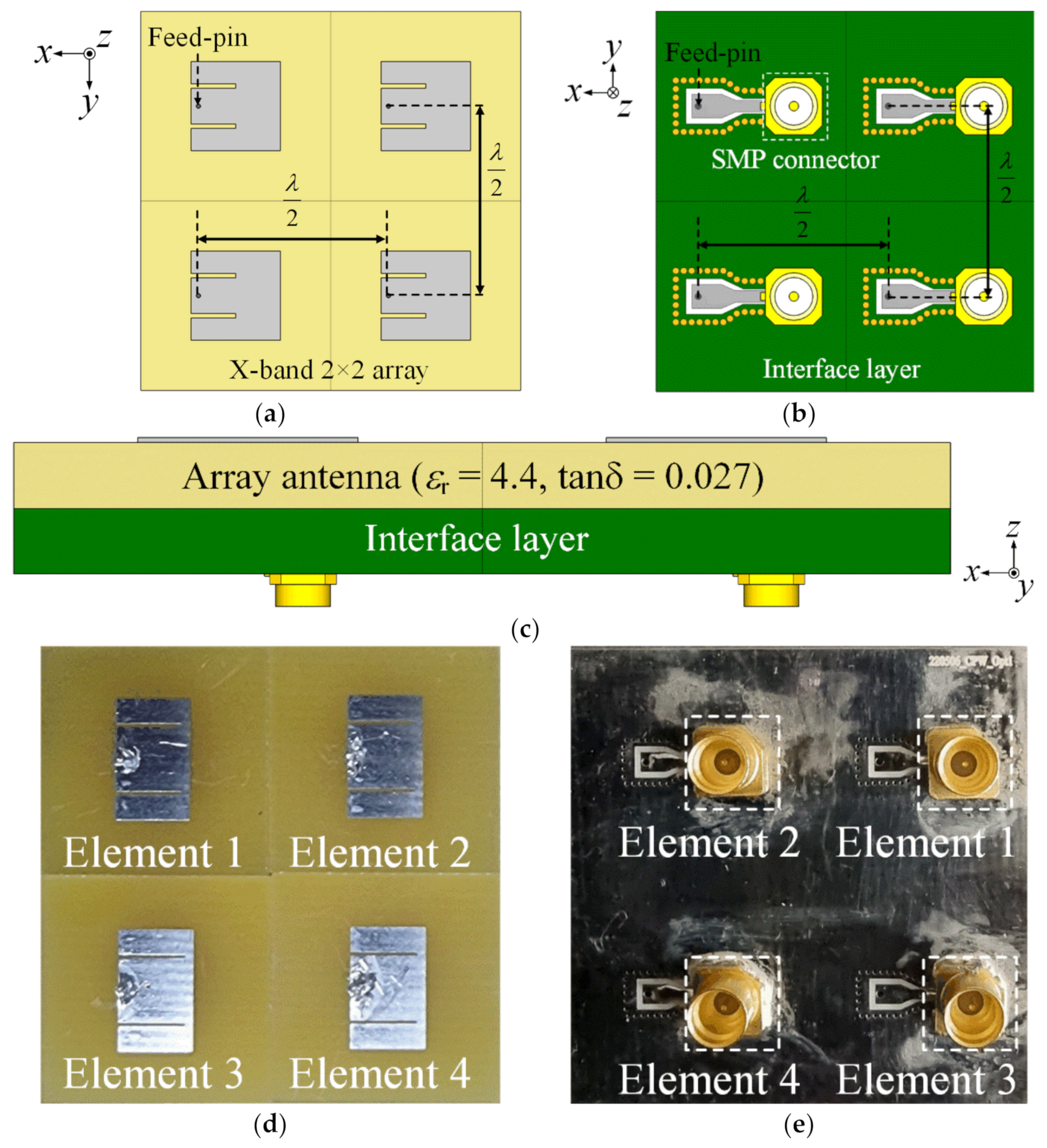
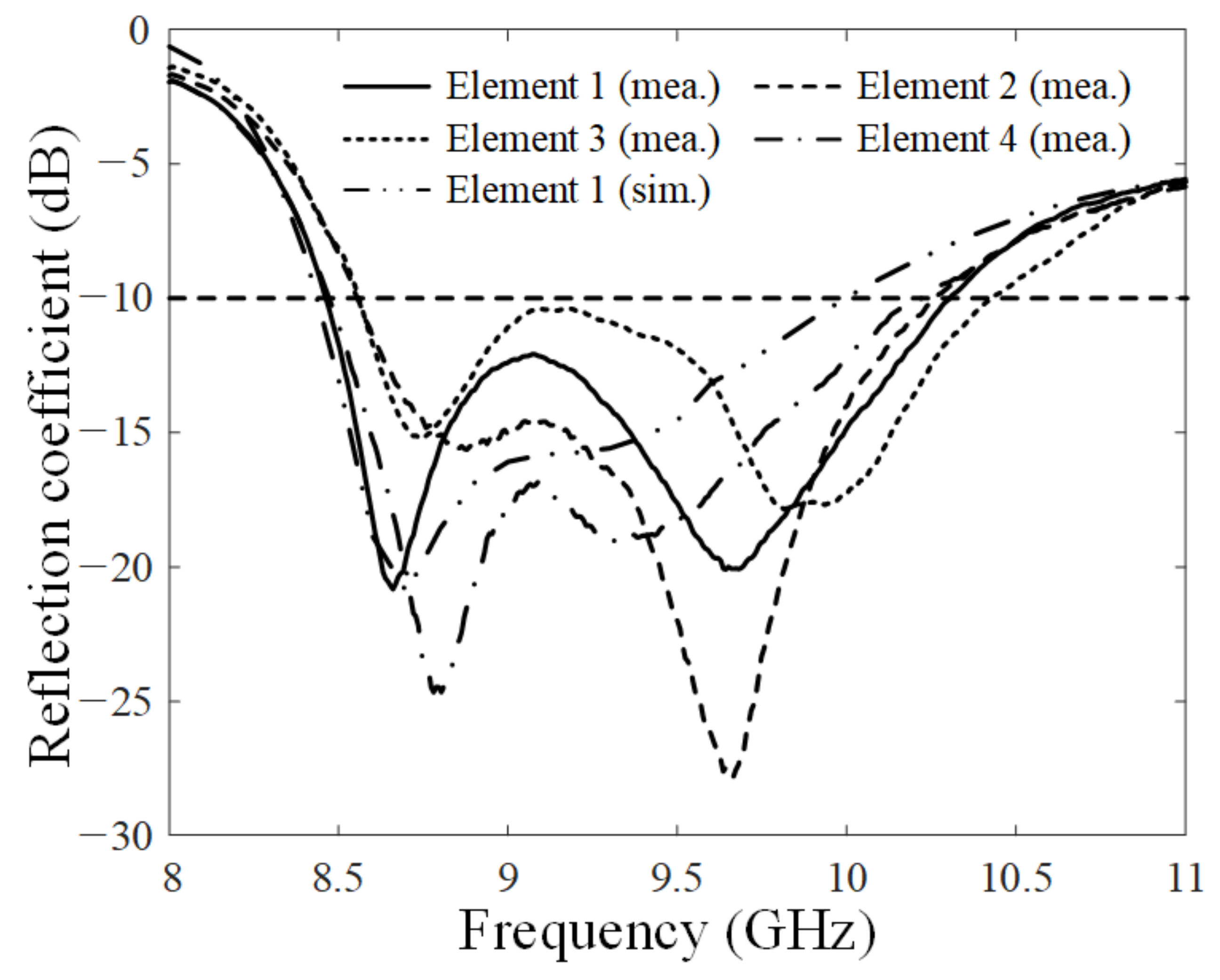
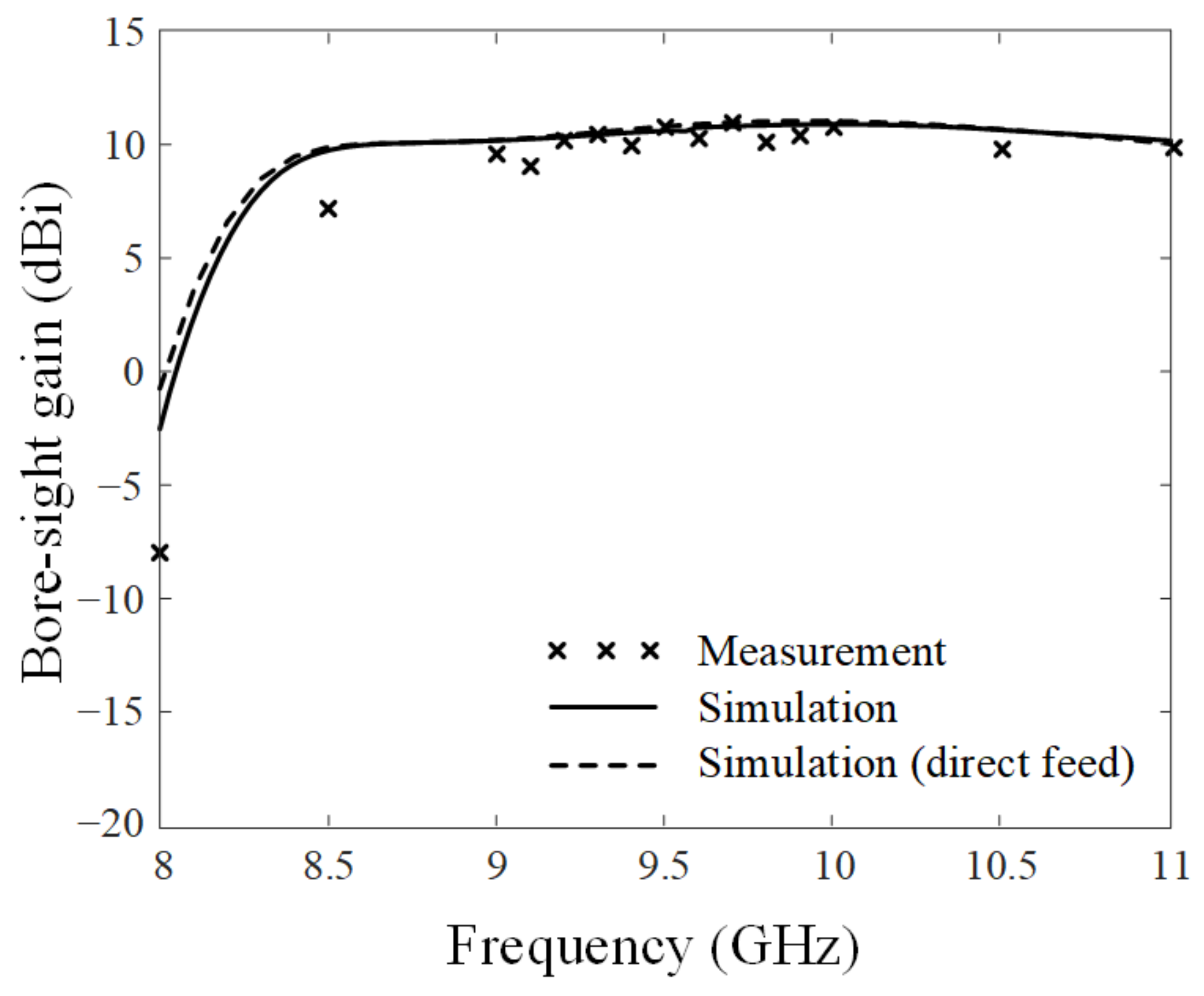
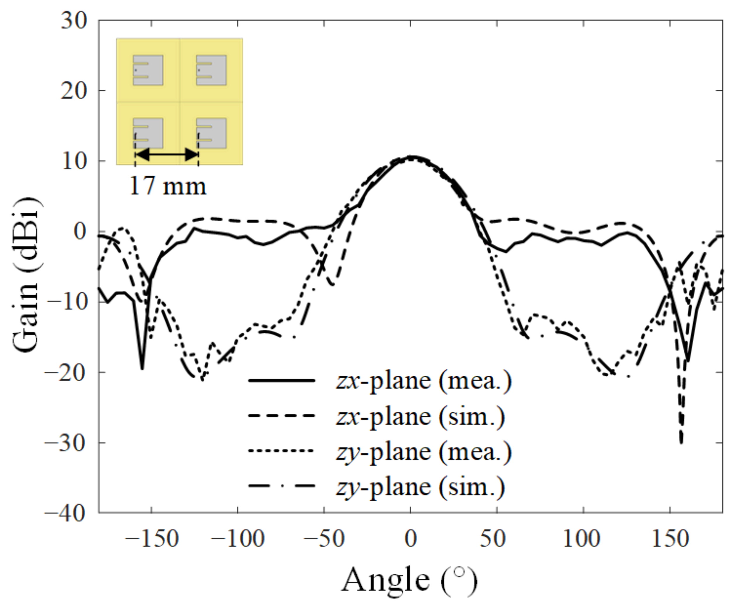
3. Verification Using an X-Band Radar Array Antenna

To verify the performance of the proposed interface layer using the CPW when it is mounted on an actual radar system, the proposed interface layer was combined with X-band E-shape antennas [26] that can operate in broadband. Figure 7a–c show the geometry of the 2 × 2 E-shape patch array for X-band radar systems. In this configuration, the array spacing was determined to be a half-wavelength at 9.5 GHz, and the interface layer using the CPW was placed in the bottom layer. Figure 7d,e show photographs of a fabricated 2 × 2 array antenna to assess the performance of the proposed interface layer. The fabricated 2 × 2 array antenna with the interface layer was measured in a full anechoic chamber to obtain the reflection coefficients of the array elements and the array beam patterns. Figure 7e does not include a feeding network, and during measurements, a feed line was connected to each port of the array to obtain the array gain. Figure 8 represents the reflection coefficients of the 2 × 2 array antenna in the X-band. The measured reflection coefficients for each element had a broad bandwidth greater than the frequency range from 8.6 GHz to 10.2 GHz and were consistent with the simulation results. Figure 9 shows the measured and simulated bore-sight gains of the 2 × 2 array with and without the interface layer. The solid line is the simulation result with the interface layer, and the dashed line is the result without the interface layer. The ‘×’ markers indicate the measurement with the interface layer. The measured results agreed well with the simulations. The array antenna gains with and without the interface layer were greater than 10.1 dBi in the target frequency range from 9 GHz to 10 GHz. Figure 10 illustrates the measured and simulated 2-D array beam patterns of the 2 × 2 array antenna in the zx- and zy-planes at 9.5 GHz. The bore-sight gains were 10.5 dBi for the measurement and 10.6 dBi for the simulation. In addition, the half-power beamwidths (HPBWs) were 47.8° and 39.1° in the zx- and zy-planes, and simulated HPBWs were 46.5° and 40.3° in the zx- and zy-planes, respectively. Thus, the measurement results for the 2 × 2 arrays with the interface layer were in good agreement with the simulation results. These results demonstrate that the proposed interface layer using the CPW can be applied to X-band marine radar systems.

4. Conclusions

We investigated the interface layer using the CPW in X-band radar systems to minimize the leakage electric fields and improve the transmission characteristics. To prevent performance degradation in the radar systems, the interface layer with the CPW had three transition parts. Transition part A was between the SMP connector and the interface layer. Transition part B was the CPW in which the thickness gradually increased. Transition part C was for connecting the interface layer and the antenna. In addition, we proposed the interface layer using the CPW in the back-to-back configuration, which could observe the performance deteriorations caused by the interface layer in the radar systems. The reflection and transmission coefficients layer in the back-to-back configuration were measured to be −22.4 dB and −0.82 dB, respectively. To examine the performance when the interface layer using CPW was mounted on the actual radar systems, X-band 2 × 2 E-shape antennas with broadband characteristics were connected to the proposed interface layer. The bore-sight gain of the 2 × 2 array antenna was 10.5 dBi at 9.5 GHz. In addition, the HPBWs under the same conditions were 47.8° and 39.1° in the zx- and zy-planes, which are in good agreement with the simulated results. The results demonstrated that the proposed interface layer using the CPW was suitable for X-band marine radar systems.

Author Contributions

Conceptualization, J.C., D.J. and H.C.; methodology, J.C., D.J., C.-H.L. and H.C.; software, J.C. and D.J.; validation, D.J., C.-H.L. and H.C.; formal analysis, J.C., D.J. and H.C.; investigation, J.C. and D.J.; resources, J.C., D.J., C.-H.L. and H.C.; writing—original draft preparation, J.C. and D.J.; writing—review and editing, J.C., D.J. and H.C.; visualization, J.C. and D.J.; supervision, H.C.; project administration, H.C. All authors have read and agreed to the published version of the manuscript.

Funding

This research received no external funding.

Institutional Review Board Statement

Not applicable.

Informed Consent Statement

Not applicable.

Data Availability Statement

Not applicable.

Acknowledgments

This research has been supported by the Challenging Future Defense Technology Research and Development Program (9127786) of Agency for Defense Development in 2019.

Conflicts of Interest

The authors declare no conflict of interest.

References

  1. Pehlivan, M.; Yegin, K. X-band low-probability intercept marine radar antenna design with improved bandwidth and high isolation. IEEE Trans. Antennas Propag. 2021, 69, 8949–8954. [Google Scholar] [CrossRef]
  2. Wang, Z.; Zhou, J.; Wang, Y.-N.; Zhu, Z.; Fang, S.; Liu, H. A compact feeding network with radiation contribution for X-band marine radar antenna array applications. Microw. Opt. Technol. Lett. 2019, 61, 2819–2825. [Google Scholar] [CrossRef]
  3. Huang, W.; Liu, X.; Gill, E.W. Ocean wind and wave measurements using X-band marine radar: A comprehensive review. Remote Sens. 2017, 9, 1261. [Google Scholar] [CrossRef]
  4. Lu, K.; Leung, K.W.; Yang, N. 3-D-Printed circularly polarized twisted-ridge horn antenna. IEEE Trans. Antennas Propag. 2021, 69, 1746–1750. [Google Scholar] [CrossRef]
  5. Manshari, S.; Koziel, S.; Leifsson, L. A wideband corrugated ridged horn antenna with enhanced gain and stable phase center for X- and Ku-band applications. IEEE Antennas Wirel. Propag. Lett. 2019, 18, 1031–1035. [Google Scholar] [CrossRef]
  6. Ur-Rehman, M.; Safdar, G.A.; Yang, X.; Chen, X. Design and study of a circular polarised conical-disc-backed spiral antenna for X-band applications. IEEE Access 2017, 5, 21344–21354. [Google Scholar] [CrossRef]
  7. Zhai, H.; Tjuatja, S.; Bredow, J.W.; Lu, M. A quasi-planar conical antenna with broad bandwidth and omnidirectional pattern for ultrawideband radar sensor network applications. IEEE Trans. Antennas Propag. 2010, 58, 3480–3489. [Google Scholar] [CrossRef]
  8. Rajesh, N.; Malathi, K.; Raju, S.; Kumar, V.A.; Prasath, S.D.R.; Alsath, M.G.N. Design of Vivaldi antenna with wideband radar cross section reduction. IEEE Trans. Antennas Propag. 2017, 65, 2102–2105. [Google Scholar] [CrossRef]
  9. Bang, J.; Lee, J.; Choi, J. Design of a wideband antipodal Vivaldi antenna with an asymmetric parasitic patch. J. Electromagn. Eng. Sci. 2018, 18, 29–34. [Google Scholar] [CrossRef]
  10. Yan, J.-B.; Gogineni, S.; Camps-Raga, B.; Brozena, J. A dual-polarized 2–18-GHz Vivaldi array for airborne radar measurements of snow. IEEE Trans. Antennas Propag. 2016, 64, 781–785. [Google Scholar] [CrossRef]
  11. Jeon, G.-H.; Dzagbletey, P.A.; Chung, J.-Y. A cross-joint Vivaldi antenna pair for dual-pol and broadband testing capabilities. J. Electromagn. Eng. Sci. 2021, 21, 201–209. [Google Scholar] [CrossRef]
  12. Jang, D.; Lim, T.H.; Kim, D.; Wang, S.; Choo, H. Design of a high-durability X-band patch antenna with a CPW feeding network based on a durability evaluation analysis. Electronics 2022, 11, 553. [Google Scholar] [CrossRef]
  13. Kuo, F.-Y.; Hwang, R.-B. High-isolation X-band marine radar antenna design. IEEE Trans. Antennas Propag. 2014, 62, 2331–2337. [Google Scholar]
  14. Bilgic, M.M.; Yegin, K. Wideband offset slot-coupled patch antenna array for X/Ku-band multimode radars. IEEE Antennas Wirel. Propag. Lett. 2014, 13, 157–160. [Google Scholar] [CrossRef]
  15. Rana, B.; Lee, I.-G.; Hong, I.-P. Experimental characterization of 2 × 2 electronically reconfigurable 1 bit unit cells for a beamforming transmitarray at X band. J. Electromagn. Eng. Sci. 2021, 21, 153–160. [Google Scholar] [CrossRef]
  16. Carlofelice, A.D.; Paulis, F.D.; Fina, A.; Marcantonio, U.D.; Orlandi, A.; Tognolatti, P. Compact and reliable T/R module prototype for advanced space active electronically steerable antenna in 3-D LTCC technology. IEEE Trans. Microw. Theory Tech. 2018, 66, 2746–2756. [Google Scholar] [CrossRef]
  17. Wang, S.; Qi, H.; Yu, W. Polarimetric SAR internal calibration scheme based on T/R module orthogonal phase coding. IEEE Trans. Geosci. Remote Sens. 2009, 47, 3969–3980. [Google Scholar] [CrossRef]
  18. Makhoul, E.; Broquetas, A.; Lopez-Dekker, F.; Closa, J.; Saameno, P. Evaluation of the internal calibration methodologies for spaceborne synthetic aperture radars with active phased array antennas. IEEE J. Sel. Top. Appl. Earth Observ. Remote Sens. 2012, 5, 909–918. [Google Scholar] [CrossRef]
  19. Fina, A.; Carlofelice, A.D.; Paulis, F.D. High power, thermally efficient, X-band 3D T/R module with calibration capability for space radar. IEEE Access 2018, 6, 60921–60929. [Google Scholar] [CrossRef]
  20. Yeo, S.-K.; Chun, J.-H.; Kwon, Y.-S. A 3-D X-band T/R Module package with an anodized aluminum multilayer substrate for phased array radar applications. IEEE Trans. Adv. Packag. 2010, 33, 883–891. [Google Scholar] [CrossRef]
  21. Yu, Z.-J.; Xu, Z.; Deng, Y.-K.; Zhang, Z.-G. An overall LTCC package solution for X-band tile T/R module. Prog. Electromagn. Res. Lett. 2013, 38, 181–192. [Google Scholar] [CrossRef] [Green Version]
  22. Ortiz, J.A.; Salazar-Cerreno, J.L.; Diaz, J.D.; Lebron, R.M.; Aboserwal, N.A.; Jeon, L. Low-cost CMOS active array solution for highly dense X-band weather radar network. IEEE Trans. Antennas Propag. 2020, 68, 5421–5430. [Google Scholar] [CrossRef]
  23. Jidi, L.; Cao, X.; Li, W.; Gao, J.; Zheng, Y.; Li, T.; Tang, Y. X-band and circularly polarized antenna with inborn RCS reduction. IEEE Antennas Wirel. Propag. Lett. 2018, 17, 1501–1504. [Google Scholar] [CrossRef]
  24. SMP-MSSB-PCS15T, Amphenol RF. Available online: https://kr.mouser.com/manufacturer/amphenolrf/ (accessed on 1 November 2021).
  25. FEKO EM Software, Altair. Available online: https://www.altair.co.kr/feko/ (accessed on 1 November 2021).
  26. Wang, S.; Kim, H.; Kim, H.; Choo, H. Design of a polarization-selective EM transparent mesh-type E-shaped antenna for shared-aperture radar applications. Appl. Sci. 2022, 12, 1862. [Google Scholar] [CrossRef]
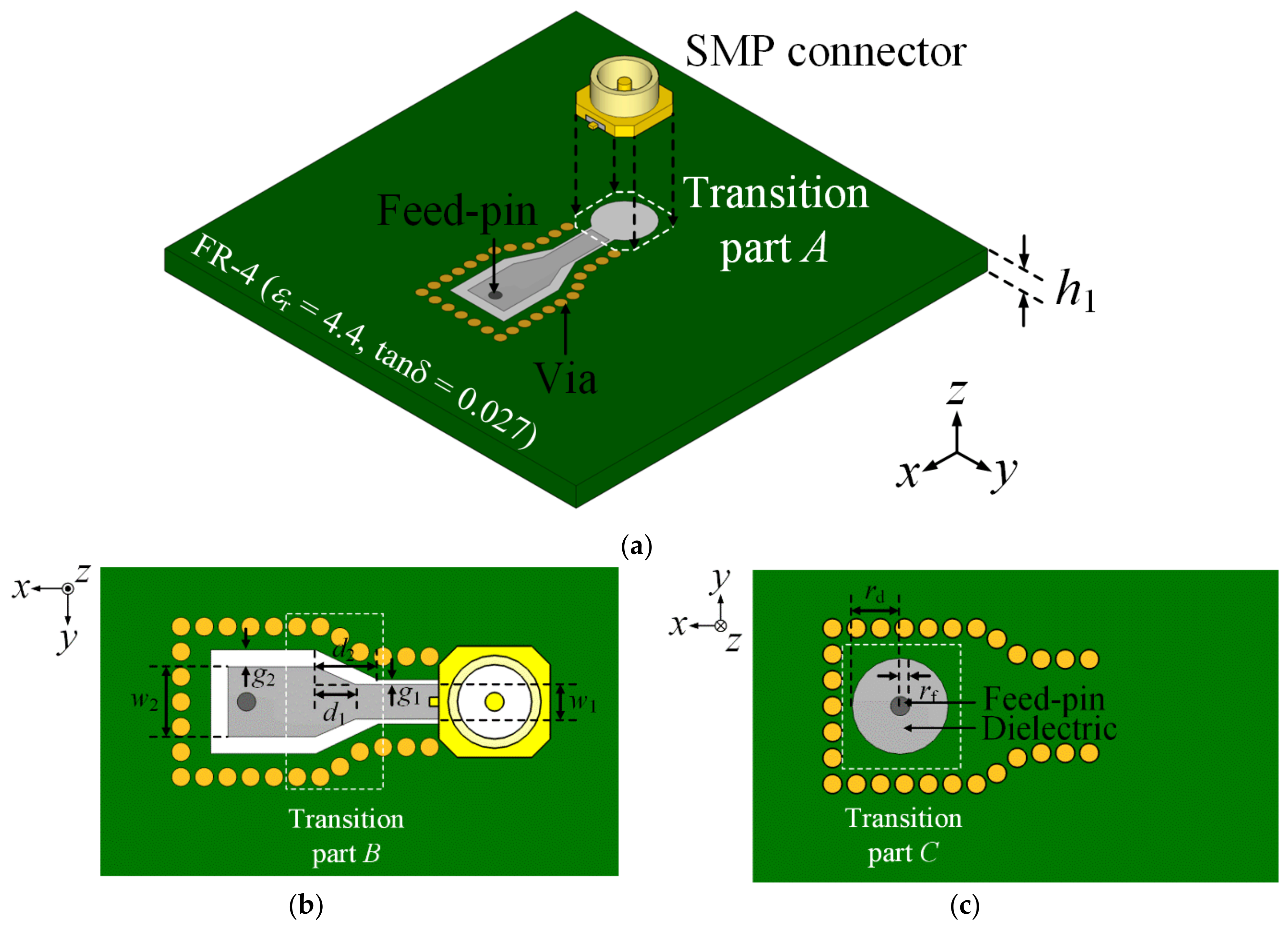
Figure 1. Geometry of the proposed interface layer using the CPW: (a) isometric view; (b) top view; (c) bottom view.
Applsci 12 08514 g001
Figure 2. Photograph of the proposed interface layer and back-to-back configuration: (a) top view; (b) bottom view; (c) geometry of the back-to-back configuration; (d) fabrication of the back-to-back configuration.
Applsci 12 08514 g002aApplsci 12 08514 g002b
Figure 3. Reflection and transmission coefficients of the proposed interface layer in the back-to-back configuration.
Applsci 12 08514 g003
Figure 4. The normalized E-field distributions of the interface layer: (a) without ground; (b) with ground but without vias; (c) with ground and vias (proposed interface layer).
Applsci 12 08514 g004aApplsci 12 08514 g004b
Figure 5. The reflection coefficients in accordance with d1 and d2 in transition part B.
Applsci 12 08514 g005
Figure 6. The reflection coefficients in accordance with rf and rd in transition part C.
Applsci 12 08514 g006
Figure 7. Geometry and fabrication of the 2 × 2 E-shape array antennas with the proposed interface layer: (a) isometric view; (b) top view; (c) side view; (d) top view photograph; (e) bottom view photograph.
Applsci 12 08514 g007
Figure 8. Reflection coefficients of the 2 × 2 X-band array.
Applsci 12 08514 g008
Figure 9. Bore-sight gain of the 2 × 2 array.
Applsci 12 08514 g009
Figure 10. Array beam patterns of the 2 × 2 X-band array.
Applsci 12 08514 g010
Table 1. Optimal design parameters of the interface layer.
ParameterValue (mm)
h10.8
w10.75
w21.5
g10.1
g20.37
d10.85
d21.35
rf0.22
rd1.3
Publisher’s Note: MDPI stays neutral with regard to jurisdictional claims in published maps and institutional affiliations.

