1. Introduction
Equipment and devices can fail during their operation in the field and this may occur prematurely. Such a premature failure can render inconveniences and even safety concerns because the failures are unexpected. To prevent the reoccurrence of the failures, a root cause analysis is important. There are differences between failure modes, failure mechanisms, and root causes. An example is an open circuit (failure mode) caused by conductor corrosion (failure mechanism) due to an incomplete protective coating (root cause). Whilst the identification of failure modes can be easy because they can be seen or measured, the finding of failure mechanisms and subsequent root causes are not trivial.
Printed circuit boards (PCBs) are essential for all electronics. They provide mechanical support and electrical connections to the electronic components of an electronic system. As electronic controls and the internet become essential, many public transport systems contain several PCBs. However, the operating environment in public transport can be harsh due to cyclic temperature and humidity, especially in regions with four different weather seasons.
PCB failures range from circuit malfunctions to propagating PCB faults. PCB failures that may appear similar can originate from many different root causes. A propagating circuit board fault is usually considered universally to be a high severity thermal event. Its initiating mechanism starts when a resistive path forms between two traces or planes in a PCB that are at a different electric potential. This resistive path can form due to an external heat source [
1], insulation breakdown [
2], arcing [
3], or contamination [
4]. The power dissipated at the fault region should be sufficient to generate enough heat to further damage the PCB and sustain the thermal event [
1]. Slee et al. [
1] described various causes of propagating faults in PCBs; namely, resistive heating, interconnect overheating, contamination, electrochemical migration, tin whiskers, insulation failure, and component failure.
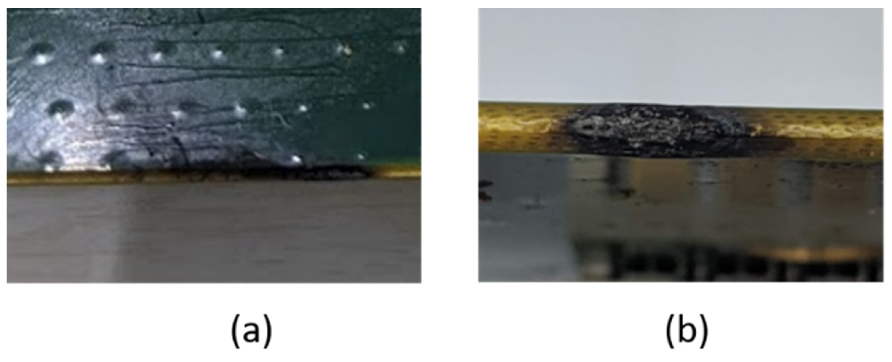
In this work, a propagating fault reported was due to electrochemical migration. We report our steps of tracing from the failure modes to the root cause of a PCB used in public transport for an ethernet connection. After their operation for 1.5 months, the operations of the ethernet device stopped and the burn-out area at the bottom edge of the PCB was found, as shown in
Figure 1.
These PCBs have multilayers that consist of 8 layers with 2 mm of total thickness. Layer 4 is the electrical ground plane and layer 5 is the power plane (VIN) where 12 V is connected to it. Its base material is FR4 (flame retardant). This PCB had superior CAF (conductive anodic filament)-resistance (anti-migration) properties and a high glass transition temperature (Tg) (minimum 170 °C), which makes it a better candidate in the comparison of a standard FR4 for applications where high mechanical and chemical resistances to heat and moisture properties are required.
2. Identification of the Failure Modes
A PCB was returned from customers due to burn-out, as shown in
Figure 1. Upon detailed measurements, it was found that the impedance between V
IN and GND significantly dropped. A similar burn-out as in
Figure 1 was observed on a few originally good inventory boards after testing them with the system in the factory. The supply current was monitored to avoid severe damage to the testing PCBs. It was found that, after the initial short-circuited event, the burn-out expanded due to the over current protection (OCP) mechanisms in the power module. These OCPs are for the protection of the power supply. Two mechanisms are employed for the OCP; namely, the cycle-by-cycle current limit and the cycle skip.
The cycle-by-cycle current limit turns off the power if the maximum current within each pulse width modulation (PWM) cycle is exceeded. The company set the maximum current threshold to 8 A as the continued working current. However, the actual maximum current could be larger than this value due to the response delay; the magnitude depends on the load condition.
The cycle skip mechanism is activated by the continuous occurrence of a cycle-by-cycle current limit condition. The PWM enters into a silent period then restarts the powering cycle again. The company set the continuous occurrence time and the silent period to 30 ms and 250 ms, respectively.
These power supply protection mechanisms can continuously deliver 8.5 W under a short-circuit condition.
3. Identification of the Failure Mechanism
To understand the failure mechanism, a detailed failure analysis was performed. To begin, the structure of the PCB near the burn-out area was studied, as shown in
Figure 2. A V-groove penalization was used here; it can protect the PCBs from shocks and vibration experienced during paste printing to component assembly, soldering, and even testing [
5].
After the PCB fabrication processes are completed, de-penalization is performed to split them into individual PCBs. Currently, there are various types of de-penalization; namely, hand break, pizza cutter/V-cut, punch, router, saw, and laser [
5]. In this work, a pizza cutter/V-cut was employed for the de-penalization.
Upon careful examination of the PCBs that were not short-circuited or burned out, the presence of many crack lines could be seen (
Figure 3). These crack lines were found after the de-penalization. With these crack lines, moisture from the environment could penetrate and diffuse into the PCB easily. In the presence of the applied voltage, the electric field could cause the copper ions from the PCB copper planes to drift across either as a dendrite formation [
1,
5,
6,
7,
8] or as a CAF formation [
9,
10]. This was believed to be the failure mechanism.
Dendritic growth usually occurs when metal ions move into the electrolyte layer near the anode and then deposit near the cathode and grow in a tree-like or needle-like formation. IPC-5704 defines dendritic growth as the growth of conductive metal filaments on a PCB through an electrolytic solution under the influence of a DC voltage bias and it is usually formed on the surface of a PCB [
11]. Heat can be generated from the electrical ionic conduction current during the migration process or from the electrical current conducted through the dendrites when they bridge the conductors. Eventually, the dendrites can develop into substantially low resistance with significant heat dissipation and can result in a propagating fault in a PCB [
1].
The CAFs are formed as anode metal gradually becomes ions and begins to migrate under the effects of the bias voltage. It is formed within the PCB insulation materials. Unlike dendrite formation, the conductive filament growth forms from the anode to the cathode, hence the name conductive anodic filament [
1]. Failure symptoms of a CAF range from intermittent resistive faults under current limit conditions to catastrophic propagating circuit board faults if the fault current is not sufficiently limited [
1]. Basically, CAF formation follows a two-step process; namely, the formation of a microcrack that bridges two conductors to establish the migration path and an electrochemical reaction with the presence of a DC bias and moisture to drive the migration along the cracks between the two conductors [
12]. This was observed in our experiments, as will be shown later.
The formation of dendrites and CAFs can seriously influence the reliability of electronic systems. From our failure analysis observations, the failure mechanism was likely to be a CAF as the short-circuit paths were not on the surface although this PCB was CAF-resistant.
4. Mechanism of the Copper Particles in the FR4 during CAF
Due to the presence of moisture and an electric field, copper ions will migrate along the glass fiber. This is a well-established phenomenon in PCBs known as CAF. As copper ions move, and as it is known that conductive particles exposed to an applied electric field will be charged [
13,
14], these copper ions will also be charged. As the charged particles move, they also induce a current through the external circuit [
15] and, in the case of partial discharge (which will be described later), a very short pulse of current will be induced as there will be a charge transfer between the particle and the facing electrode, which is the cathode [
16].
Generally, conductive particles in the presence of an electric field and fluid such as water will be subjected to various forces including a drift electric force, fluid force, and gravity force. The fluid force includes a mass force, drag force, and Basset force. For a detailed study of the forces, one may refer to the work by Pan et al. [
17]. Although the work by Pan is for conductive particles in liquids, several of the underlying physical mechanisms considered can be applied. In the situation studied in this work, due to its mass and density, the copper particles were only subjected to the drift electric force and no rebound between the two electrodes occurred.
As the conductive particles are close to the cathode as driven by the electric field from the anode to the cathode, partial discharge can occur due to the intensification of the electric field between them [
17]. It has been found that the electric field is enhanced by 4.2 times for a spherical particle [
16]. In the presence of multiple conductive particles, as in our case, the frequency of the partial discharge can be much higher, as shown by Li et al. [
18].
However, partial discharge does not necessary lead to the breakdown of the dielectric but it will lead to the reduction of its breakdown voltage. As the size and concentration of the particles increase, the insulating performance of the dielectric is further inhibited [
19,
20,
21]. With the reduction in the insulating performance, a leakage current can flow through the FR4 and generate heat. It is worth noting that if the temperature around the FR4 exceeds more than 65 °C, heat dissipation becomes a major issue for the FR4; beyond this temperature, the failure mechanism changes to a thermal breakdown from an electric breakdown [
2].
When the particle concentration is relatively high, the formation of a particle bridge is possible. It was found that a DC field is beneficial to such a formation, as shown by the work by Li et al. [
22].
After a partial discharge, it is suspected that a short carbonization path is formed that connects the conductive particles to the nearby electrode [
2,
23]. In a sense, the electrode is now extruded. Hence, the conductive particles that are further away can now also have a partial discharge with the subsequent formation of a carbonization path. When the resistance reduces to a certain value that corresponds with an increase in the leakage current, the Joule heating can drive out the surrounding moisture and an increase in resistance can be expected, as was observed in our experiments (shown later in
Section 7) However, the charge relaxation on the conductive particles may also be reduced and thus the movement of the charged conductive particles can move further. At the same time, this localized heat enlarges the crack. Hence, external moisture can now diffuse further and in a greater amount into the FR4. As the conductive particles move closer to the extruded electrode, partial discharge occurs again. This iteration continues until the effective distance between the extruded electrode and the anode becomes so close that the field between them is so high, it exceeds the breakdown field of the FR4, which is already reduced due to the presence of conductive particles and carbonization.
5. Experimental Results and Discussion
To confirm the proposed mechanism, a Thermo Scientific ELITE VX system was used to identify the hot spot of the thermal emissions and a 3D X-ray was performed using ZEISS Xradia 520 Versa on the hot spot.
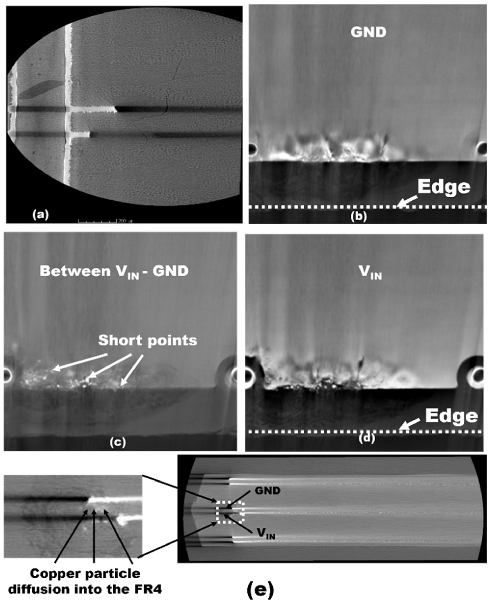
Figure 4 shows the enlarged X-ray micrograph at the hot spot in the burn-out area and we can clearly see that the short-circuit was due to copper particles at the edge of the PCB along the de-penalized line. From the cross-sectional view of the X-ray micrograph, one can see that the trace of copper is indeed from the V
IN (anode) toward the GND (ground).
To further analyze and characterize the cracks formed in the PCB, as shown in
Figure 4, the PCB area with the cracks was dissected out and examined under an X-ray Micro CT (computed tomography) scanner system (model number CTLab-HX130-2-E). The dissection was needed due to the size limitation of the X-ray system. For a better view of the cracks, the image dataset was reoriented with a new image plane, as shown by the pink color plane in the top left side image in
Figure 5. In
Figure 5 (top left), ‘a’, ‘b’, and ‘c’ are marked to show the front, top, and left sides, respectively, and their respective 2D images are shown in the same figure.
A total of 78 cracks were identified, and these cracks are shown by their individual colors in
Figure 6. The histogram of the volume of these cracks is shown in
Figure 7a, which shows that the majority of the cracks (25) had a volume less than 1 × 10
5 (μm
3). No crack had a volume greater than 4 × 10
5 (μm
3).
Figure 7b shows all the identified cracks and the cracks with the same volume are shown with the same colors in the 3D view. It could be observed that large cracks occurred at the edge of the PCB and they progressed toward the inner parts of the PCB along with the GND and V
IN layers. All these cracks were due to excessive high strain at a high strain rate induced during the V-cut de-panelization as measured experimentally with the results shown in
Figure 8. The experimentation is discussed in the next section.
The large cracks observed were concentrated in a certain area of the PCB instead of being distributed uniformly. This non-uniform distribution of the crack sizes was believed to be due to the inhomogeneous strain distribution along the edge of the PCB during the V-cut de-panelization as simulated using a finite element analysis, which will be discussed in the next section. There were also large cracks present away from the edge but they were closed to the largest cracks, indicating the weakening of the mechanical integrity of the board after the large cracks occurred.
To further confirm the proposed mechanism, 5 samples of the PCB that had crack lines due to de-penalization were subjected to 65 °C/95% RH.
Table 1 summarizes the test results. The test condition was selected so that a continuous film of water could be formed in the PCB. The test results showed clearly that these cracks allowed moisture to diffuse into the PCB and reduced the impedance between the GND and V
IN.
From the above observations, the failure mechanism could be summarized, as shown in
Figure 9. The flow chart and its summary table to represent the research methodology of this work are shown in
Figure 10 and
Table 2, respectively.
6. Possible Root Causes and Their Verification
Knowing that it was the crack lines that caused the observed failure mode, and that these lines were generated because of the high strain developed during the de-penalization process, a strain gauge measurement was performed on the PCB at three test locations, as marked by the black color blocks in
Figure 11, near the edge of the PCB during the V-cutting process to ascertain the root cause. The strain gauge measurement results are depicted in
Figure 8. One can see the localized areas along the de-paneling line at the bottom side with a high strain rate and high strain around 1400–2050, which was beyond the acceptable criteria according to IPC-WP-011 [
24].
ANSYS WorkBench 19.0 was also employed to examine the strain induced by de-penalization. A 3D CAD model of the PCB was designed in ANSYS WorkBench and a V-cut cutter was designed to mimic the real-world scenario in the simulation software where mechanical strain was observed, as shown in
Figure 11. Our simulation results showed the maximum stress area (red area) distributed in strips along the edge of the PCB and this coincided with the burn-out area. The maximum strains did not distribute uniformly, which agreed with our X-ray micrograph and the strain gauge measurement results. Li [
25] also reported that the stress generated through the V-cut process is significantly high in comparison with other cutting processes that cause mechanical cracks in PCBs.
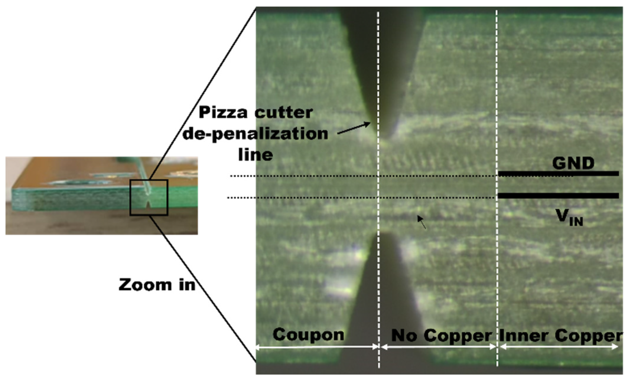
In the pizza cut de-penalizing, the applied mechanical stress caused cracks on the copper keep-out area of the PCB, as shown in
Figure 12. However, without de-paneling, there was no crack on the copper keep-out area, as can be seen in
Figure 13.
It was, therefore, clear that it was the pizza cutter de-penalization that caused the cracks in the PCB, which then resulted in moisture diffusion into the PCB. As the cutting area was near the GND plane and V
IN plane, as can be seen in
Figure 2, the reported failure mode was observed. We found that no damage was observed if a manual de-penalization was performed. Thus, we believed that a proper V-groove design and machine setting could solve this issue, but this was beyond the scope of this work. With proper settings such as the incident angle, rotary speed, and cooling fluid, such damage can be minimized, as in the case of wafer dicing [
26].
7. Corrective Actions and Reliability Verification
With the identification of the root cause, another type of de-penalization was introduced where no crack was produced. Due to confidential considerations, this new way cannot be disclosed.
To verify the effectiveness of the corrective actions, reliability tests were performed along with the new de-penalization method. The test condition was set at 65 ℃/95% RH so that a continuous water film could be formed if cracks existed. To speed up the test, a voltage of 100 V was applied across the GND and VIN.
From
Figure 14, with the new de-penalization method, the resistance between the GND and V
IN remained high: up to 800 h of testing consistently for the 10 test samples. However, 4 PCBs with the V-cut de-penalizing methods showed a significant reduction in the resistance even before 400 h of testing, except for one board. This clearly showed that our corrective action was effective in overcoming the damage introduced due to de-penalization.
8. Conclusions
This work demonstrated a step-by-step failure analysis methodology for multilayer printed circuit boards that led an observed failure mode to the root cause with verification of the root cause and the effectiveness of the corresponding corrective action. Printed circuit boards used in public transport systems were found to be burnt after a time of operation. A detailed failure analysis showed that the failure mechanism was a propagating fault of a CAF formation as moisture was diffused into the PCBs via microcracks introduced due to a V-cut de-penalization. Although the PCB itself was CAF-resistant, the presence of a microcrack due to de-penalization could render its CAF resistance ineffective.
With the identified root cause, a modified de-penalization method was developed and no microcracks were observed with this new method, which verified the root cause. The PCBs with the modified de-penalization method also underwent reliability tests under a high temperature/humidity with a high voltage applied across and only small changes in resistance between the previously affected planes were observed, which confirmed the effectiveness of the corrective action. The detailed steps from the failure mode to the failure mechanism and from the failure mechanism to the root cause were clearly described.
Author Contributions
Methodology, C.-M.T. and J.-P.W.; formal analysis, C.-M.T., H.-H.C., J.-P.W., and V.S.; investigation, C.-M.T., J.-P.W., and V.S.; resources, H.-H.C., K.-Y.T., and W.-C.H.; writing—original draft preparation, V.S.; writing—review and editing, C.-M.T., J.-P.W., H.-H.C., and V.S.; project administration, H.-H.C. All authors have read and agreed to the published version of the manuscript.
Funding
This research received no external funding.
Acknowledgments
This research is an industrial collaboration with a company to solve a real industrial issue, leveraging on the in-depth applied failure analysis theory developed by the Centre for Reliability Science and Technology in Chang Gung University. This research did not receive any specific grants from funding agencies in the public, commercial, or not-for-profit sectors. The authors also acknowledge the support of C.Y. Hsueh from Jie Dong, Taiwan and Rigaku Corporation, Japan, in assisting with the X-ray computed tomography analysis.
Conflicts of Interest
The authors declare no conflict of interest.
References
- Slee, D.; Stepan, J.; Wei, W.; Swart, J. Introduction to printed circuit board failures. In Proceedings of the 2009 IEEE Symposium on Product Compliance Engineering, Toronto, ON, Canada, 26–28 October 2009; pp. 1–8. [Google Scholar]
- Zhou, Q.; Wen, M.; Xiong, T.; Jiang, T.; Zhou, M.; Ouyang, X.; Xing, L. Study on Insulation Breakdown Characteristics of Printed Circuit Board under Continuous Square Impulse Voltage. Energies 2018, 11, 2908. [Google Scholar] [CrossRef] [Green Version]
- Davis, J.H. Silicone protective encapsulants and coatings for electronic components and circuits. In Plastics for Electronics; Springer: Dordrecht, The Netherlands, 1985; pp. 67–97. [Google Scholar]
- Khandpur, R.S. Printed Circuit Boards: Design, Fabrication, Assembly and Testing; Tata McGraw-Hill Electronic Engineering: New York, NY, USA, 2005; ISBN 0071589252. [Google Scholar]
- Coombs, C.F.J.; Holden, H.T. Printed Circuits Handbook, 7th ed.; McGraw-Hill Education: New York, NY, USA, 2016. [Google Scholar]
- Minzari, D.; Jellesen, M.S.; Møller, P.; Ambat, R. On the electrochemical migration mechanism of tin in electronics. Corros. Sci. 2011, 53, 3366–3379. [Google Scholar] [CrossRef]
- Yang, S.; Wu, J.; Christou, A. Initial stage of silver electrochemical migration degradation. Microelectron. Reliab. 2006, 46, 1915–1921. [Google Scholar] [CrossRef]
- Lee, S.B.; Jung, M.S.; Lee, H.Y.; Kang, T.; Joo, Y.C. Effect of bias voltage on the electrochemical migration behaviors of Sn and Pb. IEEE Trans. Device Mater. Reliab. 2009, 9, 483–488. [Google Scholar] [CrossRef]
- Tan, C.M.; Narula, U.; Seow, G.L.; Sangwan, V.; Chen, C.H.; Lin, S.P.; Chen, J.Y. Moisture resistance evaluation on single electronic package moulding compound. J. Mater. Chem. C 2020, 8, 1943–1952. [Google Scholar] [CrossRef]
- Ready, W.J.; Stock, S.R.; Freeman, G.B.; Dollar, L.L.; Turbini, L.J. Microstructure of Conductive Anodic Filaments Formed during Accelerated Testing of Printed Wiring Boards. Circuit World 1995, 21, 5–9. [Google Scholar] [CrossRef]
- IPC. IPC-5704 Cleanliness Requirements for Unpopulated Printed Boards; IPC: Bannockburn, IL, USA, 2009. [Google Scholar]
- Zou, S.; Li, X.; Dong, C.; Ding, K.; Xiao, K. Electrochemical migration, whisker formation, and corrosion behavior of printed circuit board under wet H2S environment. Electrochim. Acta 2013, 114, 363–371. [Google Scholar] [CrossRef]
- Pérez, A.T. Charge and force on a conducting sphere between two parallel electrodes. J. Electrostat. 2002, 56, 199–217. [Google Scholar] [CrossRef]
- Drews, A.M.; Kowalik, M.; Bishop, K.J.M. Charge and force on a conductive sphere between two parallel electrodes: A Stokesian dynamics approach. J. Appl. Phys. 2014, 116, 074903. [Google Scholar] [CrossRef]
- Pan, C.; Wu, K.; Du, Y.; Tang, J. Comparison of Sato’s equation and Pedersen’s theory to obtain gas discharge current. IEEE Trans. Dielectr. Electr. Insul. 2016, 23, 1690–1698. [Google Scholar] [CrossRef]
- Tobazéon, R. Electrohydrodynamic behaviour of single spherical or cylindrical conducting particles in an insulating liquid subjected to a uniform DC field. J. Phys. D Appl. Phys. 1996, 29, 2595–2608. [Google Scholar] [CrossRef]
- Pan, C.; Tang, J.; Chen, G.; Zhang, Y.; Luo, X. Review about PD and breakdown induced by conductive particles in an insulating liquid. High Volt. 2020, 5, 287–297. [Google Scholar] [CrossRef]
- Li, J.; Hu, Q.; Zhao, X.; Yao, X.; Luo, Y.; Li, Y. Partial-discharge characteristics of free spherical conducting particles under AC condition in transformer oils. IEEE Trans. Power Deliv. 2011, 26, 538–546. [Google Scholar] [CrossRef]
- Zhang, J.; Wang, F.; Li, J.; Ran, H.; Huang, D. Influence of copper particles on breakdown voltage and frequency-dependent dielectric property of vegetable insulating oil. Energies 2017, 10, 938. [Google Scholar] [CrossRef] [Green Version]
- Wang, K.; Wang, F.; Li, J.; Zhao, Q.; Wen, G.; Zhang, T. Effect of metal particles on the electrical properties of mineral and natural ester oils. IEEE Trans. Dielectr. Electr. Insul. 2018, 25, 1621–1627. [Google Scholar] [CrossRef]
- Wang, X.; Wang, Z.D. Study of dielectric behavior of ester transformer liquids under ac voltage. IEEE Trans. Dielectr. Electr. Insul. 2012, 19, 1916–1925. [Google Scholar] [CrossRef]
- Li, Y. Motion Characteristics of Solid Particles in Insulating Oil and Their Influence on Breakdown Voltage of Insulating Oil. Master’s Thesis, Chongqing University, Chongqing, China, 2017. [Google Scholar]
- ECSS. European Cooperation for Space Standardization Space Engineering: High Voltage Engineering and Design Handbook; ECSS: Noordwijk, The Netherlands, 2012. [Google Scholar]
- IPC. IPC-WP-011 Guidance for Strain Gage Limits for Printed Circuit Assemblies; IPC: Bannockburn, IL, USA, 2012. [Google Scholar]
- Li, W.; Sun, X. An analysis case on the failure of BGA solder joints. In Proceedings of the 18th International Conference on Electronic Packaging Technology, ICEPT 2017, Harbin, China, 16–19 August 2017; pp. 731–734. [Google Scholar]
- Shi, K.W.; Yow, K.Y. The characteristics and factors of a wafer dicing blade and its optimized interactions required for singulating high metal stack lowk wafers. In Proceedings of the 2013 IEEE 15th Electronics Packaging Technology Conference, EPTC 2013, Singapore, 11–13 December 2013; pp. 208–212. [Google Scholar]
Figure 1.
Visual inspection of failed PCBs: (a) top view; (b) side view.
Figure 1.
Visual inspection of failed PCBs: (a) top view; (b) side view.
Figure 2.
Cross-section of the board near the V-cut scoring area.
Figure 2.
Cross-section of the board near the V-cut scoring area.
Figure 3.
Cross-section of the PCB: (a) potential crack location; (b) after pizza cutter (V-cut) de-panel process.
Figure 3.
Cross-section of the PCB: (a) potential crack location; (b) after pizza cutter (V-cut) de-panel process.
Figure 4.
A 3D X-ray of the PCB that shows the cross-section of the PCB. The propagation of the cracks and the movement of copper from the VIN layer to the GND layer due to the presence of the water layer and electric field can be seen: (a) shows the formation of crack lines before the resistance between them begins to decrease; (b,d) are the plane of the GND and VIN layer, respectively, as extracted from the 3D X-ray; (c) is the plane in the middle of the GND layer and VIN layer as extracted from the 3D X-ray where the white arrows represent copper particles; (e) side view of the PCB showing the short point in between the VIN layer and GND layer.
Figure 5.
Image dataset reoriented with a new image plane as shown by the pink color in the 3D image (top left side). The 2D images are taken at the: front side (a); top side (b); left side (c).
Figure 5.
Image dataset reoriented with a new image plane as shown by the pink color in the 3D image (top left side). The 2D images are taken at the: front side (a); top side (b); left side (c).
Figure 6.
A total of 78 cracks are identified and represented by individual colors.
Figure 6.
A total of 78 cracks are identified and represented by individual colors.
Figure 7.
(
a) Volume histogram of the cracks shown in
Figure 6; (
b) cracks with the same volume are shown with the same color.
Figure 7.
(
a) Volume histogram of the cracks shown in
Figure 6; (
b) cracks with the same volume are shown with the same color.
Figure 8.
Strain gauge measurement data show that a part of the principal strain exceeds the IPC-WP-011 standard limits during the cutting process.
Figure 8.
Strain gauge measurement data show that a part of the principal strain exceeds the IPC-WP-011 standard limits during the cutting process.
Figure 9.
Failure process and the underlying mechanisms.
Figure 9.
Failure process and the underlying mechanisms.
Figure 10.
Flow chart of the failure analysis process.
Figure 10.
Flow chart of the failure analysis process.
Figure 11.
PCB de-panel process and mechanical simulation result. Locations 1, 2, and 3 show strain gauge measurement points.
Figure 11.
PCB de-panel process and mechanical simulation result. Locations 1, 2, and 3 show strain gauge measurement points.
Figure 12.
Observation of cracks in a PCB after de-paneling using an Olympus BX51 microscope at 50 × magnification of: (b) location No. 1 and (c) location No. 2, as marked in (a), which is a horizontal cross-section of a PCB with a pizza cutter de-panel.
Figure 12.
Observation of cracks in a PCB after de-paneling using an Olympus BX51 microscope at 50 × magnification of: (b) location No. 1 and (c) location No. 2, as marked in (a), which is a horizontal cross-section of a PCB with a pizza cutter de-panel.
Figure 13.
Absence of cracks in a PCB without de-paneling. Observations were performed using an Olympus BX51 microscope at 50× magnification of: (b) location No. 1 and (c) location No. 2, as marked in (a), which is a horizontal cross-section location of a PCB without a de-panel.
Figure 13.
Absence of cracks in a PCB without de-paneling. Observations were performed using an Olympus BX51 microscope at 50× magnification of: (b) location No. 1 and (c) location No. 2, as marked in (a), which is a horizontal cross-section location of a PCB without a de-panel.
Figure 14.
Resistance changes over time under the reliability test mentioned above: (a) 10 samples with the new de-penalization; (b) 5 samples with pizza cut de-penalization and the resistance fluctuation as reported earlier can be observed. The resistance in the Y-axis is in GW.
Figure 14.
Resistance changes over time under the reliability test mentioned above: (a) 10 samples with the new de-penalization; (b) 5 samples with pizza cut de-penalization and the resistance fluctuation as reported earlier can be observed. The resistance in the Y-axis is in GW.
Table 1.
Change in resistances after temperature/humidity test.
Table 1.
Change in resistances after temperature/humidity test.
| Sample # | Initial Resistance between VIN and GND (Ω) | Measured Resistance after the Specified Test Duration (Ω) | Test Duration (Hours) |
|---|
| 1 | Over 108 | 58.6 | 160 |
| 2 | Over 108 | 30.9 K | 113 |
| 3 | Over 108 | 316.2 | 90 |
| 4 | Over 108 | 1.63 K | 232 |
| 5 | Over 108 | 46.5 | 141 |
Table 2.
Summary of the failure analysis methodology.
Table 2.
Summary of the failure analysis methodology.
| Steps | Failure Analysis Methodology | Details and Findings |
|---|
| 1 | Reception of Failed Device | Customer reported unavailability of ethernet |
| 2 | Detailed Examination and Failure Mode Inspection | Burn-out area at the bottom edge of the PCB found through naked eyes. Presence of cracks observed at the burned-out area using a low- to high-definition optical microscope, thermal emissions, 3D X-ray, and X-ray Micro CT Scanning. Cracks are found in between the L4~L5 layers at the PCB edge.
|
| 3 | Failure Mechanism Proposal and Identification | Cracks are present at the PCB edge from where the moisture penetrates inside the PCB, which causes the short-circuit; the burned-out area can be observed. Conductive anodic filament (CAF) is a proposed failure mechanism. Strain produced during the V-cut de-panelization process is more than IPC-WP-011 standard limits and verified using a strain gauge measurement and an ANSYS multiphysics simulation, which are the causes behind the cracks in the PCB.
|
| 4 | Failure Mechanism Confirmation | PCBs are subjected to a 65 °C/95% RH reliability test and resistance degradation is observed, which signifies that the moisture penetrates into the PCBs through the cracks that are present in between the L4~L5 layers. |
| 5 | Corrective Action and its Effectiveness Verification | New de-panelization process is introduced. PCBs are prepared using the new de-panelization process subjected to 65 °C/95% RH. No cracks and degradation in the PCB resistance are observed
|
| Publisher’s Note: MDPI stays neutral with regard to jurisdictional claims in published maps and institutional affiliations. |
© 2022 by the authors. Licensee MDPI, Basel, Switzerland. This article is an open access article distributed under the terms and conditions of the Creative Commons Attribution (CC BY) license (https://creativecommons.org/licenses/by/4.0/).


 ,
, 


