Article

XCT and DLW: Synergies of Two Techniques at Sub-Micrometer Resolution

by
Sven Fritzsche
*,†,
Gerd-Rüdiger Jaenisch
,
Lina Pavasarytė
and
Alexander Funk
*,†
Bundesanstalt für Materialforschung und -prüfung, 12205 Berlin, Germany
*
Authors to whom correspondence should be addressed.
These authors contributed equally to this work.
Appl. Sci. 2022, 12(20), 10488; https://doi.org/10.3390/app122010488
Submission received: 25 August 2022 / Revised: 4 October 2022 / Accepted: 13 October 2022 / Published: 18 October 2022
(This article belongs to the Section Materials Science and Engineering)

Abstract

:
Direct Laser Writing (DLW) and X-ray computed tomography (XCT) both offer unique possibilities in their respective fields. DLW produces full three-dimensional (3D) polymer structures on the microscale with resolutions below 100 nm. The fabricated structures can be analysed by XCT or X-ray microscopy (XRM), which incorporates additional X-ray lenses, in three dimensions down to a minimal basic spatial resolution of about 500 nm or 50 nm, respectively. In this work, two different DLW structures are analysed via XCT. Internal defects are detected and analysed for the purpose of quality control. Defects and structures with sizes down to 1.5 µm are successfully analysed. A 3D reconstruction and internal, hidden features of the fabricated structures are shown and discussed. In a first-of-its-kind study, we demonstrate the detectability of a single-voxel line inside a fabricated structure that would not be detectable with SEM or light microscopy. Furthermore, the direct fabrication on a PET substrate is shown to overcome the high X-ray absorbance of commonly used glass substrates. Attenuation spectra of SZ2080 and glass substrates are compared to a fabrication route direct on a 170 µm PET foil. The practical aspects of XCT measurements for DLW structures on different substrates will be discussed.

1. Introduction

DLW via two-photon polymerization (2PP) can fabricate 3D objects with high resolution [1]. The technique is also called direct laser lithography or multiphoton lithography and utilises the absorption of two or more photons to create a polymerisation in a confined volume (the so-called voxel) of the photoresist [2]. Depending on the used DLW setup and photoresist, resolutions of about 50 nm lateral and 180 nm longitudinal were shown [3,4]. Hybrid polymers such as ORMOCERs [5] or SZ2080 [6,7] are used in DLW as they offer a comparatively low shrinkage together with a high precision and small feature size. Described applications range from micro-optical lenses [8,9,10,11] to microfluidic arrangements [12,13] and scaffolds for tissue engineering [14,15]. Mechanical properties such as Young’s modulus [16] or optical properties, e.g., laser-induced damage threshold (LIDT) [17,18] and refractive index [19], have been described in the literature.
To broaden the usage of DLW in industry, a clear set of tools for process control is needed as lined out by LaFratta and Malinauskas [20]. Due to the small sizes of the fabricated structures, the physical or optical analysis is challenging, and most standard imaging methods such as scanning electron microscopy (SEM) or light microscopy (LM) are not suitable to examine the complete geometry and their inner structure in detail. DLW, with described feature sizes below 100 nm [4] and the ability to construct structures in an entire three-dimensional way, optical microscopy, as well as other spectroscopy methods, comes to its limit. For light microscopy, the optical resolution is given by the Abbe diffraction limit:
d = λ 2 · N A
where d is the limit, λ is the wavelength of the light source and N A —the numerical aperture of the optical system used. For a 40× objective with a NA of 0.65 and a light source with 550 nm, the diffraction limit d is around 423 nm for a conventional optical microscopy setup. With an oil immersion objective that has a typical NA of 1.4, the limit can be lowered to 193 nm. The SEM resolution limit is below the resolution limit of the DLW technique. However, the problem remains that with LM as well as SEM, internal structures of the fabricated objects cannot be observed. For SEM, polymer structures fabricated with DLW profit from an additional sputter-coating step to avoid charging the sample. However, Raman spectroscopy can be applied to analyse the chemical composition of the polymer, e.g., the degree of conversion, as described by Suzuki et al. [21]. White Light Interferometry Microscopy has an axial resolution in the nanometer range, but it is limited to the Abbe diffraction limit in lateral resolution; additionally, only the surface of the structure can be examined. Internal structures and undercuts cannot be examined.
XCT and XRM are non-destructive testing methods with a basic spatial resolution of several hundreds to tens of nanometers [22,23], depending on the device used, and is the only technique available to study the quality of micrometer-sized 3D structures in detail. XRM includes additional lenses based on the reflective or diffraction properties of X-rays, for instance, a capillary condensor tube or a Fresnel lens [24]. Such lenses are not used in XCT setups, and the resolution limit is purely based on the X-ray tube focal spot size and/or scintillator thickness of the detector [22]. The resolution limit of XCT and XRM differs by a factor of about 10, with today’s available techniques. Note that the nominal 3D resolution of both techniques is identical to the actual 2D resolution of the acquired radiographies. Resolution, by means of the detectability of smallest sample features, is also limited by the sample/feature material, sample/feature size, an applied X-ray spectra filter, image noise, X-ray beam path opening angle and the corresponding achieved imaging setup sharpness and/or feature contrast [25]. XCT and XRM techniques are both available as commercial laboratory devices in various configurations. However, the 3D imaging methods are not yet established in the same way as a standard light or electron microscope in research facilities. The general availability of commercial XCT devices is much larger than XRM machines. Compared to commercial laboratory devices, an advanced synchrotron facility offers a brilliant, monochromatic X-ray beam [22]. Therefore, the scan time for a sample is drastically reduced. Moreover, synchrotron facilities offer open and adjustable setups to achieve cutting edge results. Additional phase contrast or grating-based dark field imaging setups can be installed to achieve different contrast tuning for certain material classes [26,27]. This is not available for commercial devices, and it is not necessarily needed, as the intrinsically X-ray absorption contrast for the two sample phases (polymer and air) analysed in the present work is expected to be sufficient. The synchrotron-based resolution limit depends on the installed X-ray setup (lenses, detector), and the limit is comparable to laboratory devices. The synchrotron facility beam time slots are limited and proposals need to be submitted. A beam time is not guaranteed. For this, synchrotron may offer advanced, fast recording and adjustable setups, but laboratory devices offer a higher availability. Note that the radiographic imaging methods can be accompanied by imaging artefacts, which may hinder a following measure of sample features [28].
For DLW products, a complete 3D view of the structure (and substrate) can be imaged by XCT/XRM. In addition, a sliced view of any written structure can be created to investigate the inner structure. Saha et al. investigated the damage threshold of photoresists due to proximity effects via XRM [29] and has shown that with an additional share of iodine in the chemical formula of the photoresist the contrast in the XRM can be fine tuned [30]. However, this is not applied in the present work, as this is not a mandatory requirement for XCT/XRM imaging. Flaws or defects can occur at different times during the DLW process. They can occur in pre-DLW structuring, for example, in the bake phase of the photoresist, during the fabrication process itself or after the process while developing the sample to remove the unwanted photoresist. To understand the presented flaws, in this work, we will provide a short introduction to DLW fabrication and the used slicing software. During the DLW process, the in situ observation possibilities are limited due to the simple visible light camera setup used similar to the setup shown by Tičkūnas [31]. Unintended defects can have multiple origins and require a complete understanding of the DLW process to trace their original source. Created flaws can be either human-related, or part of the whole DLW process.
To obtain a physical DLW structure from a 3D model, the photoresist has to be polymerised in a way that allows to reproduce the outer and inner contours of the model. The actual beam path is determined by a slicing software that cuts the 3D model in slices perpendicular to the substrate and defines the beam scanning path along the slices. The distance between the slices is called the slicing distance. The distance between the parallel beam scanning paths within a slice is the hatching distance [32]. To shorten fabrication times in FDM (Fused Deposition Modelling), the option to use an infill is widely used [33]. When using an infill, only a certain percentage of the inner volume of an object is polymerised by the laser beam in a certain pattern. In the DLW technique, the remaining (liquid) polymer is trapped inside the pre-defined set of outer walls and can be polymerised in a second polymerisation step outside the fabrication chamber after finishing the laser writing process. Optimising the beam paths during this highly complex process is a challenging task and flaws can occur, e.g., additional fabricated lines when the model is not sliced correctly.
Another driving force behind this work is the actual lack of cheap and commercially available 3D XCT testing structures (phantoms) at their resolution limit (below 2 µm feature size). Very few manufacturers that offer 3D phantoms for sub-micrometer XCT imaging are available on the market today. Two examples are presented as a reference, the Micro-CT Bar Pattern Phantoms by QRM [34] and the Spatial Targets by Aletheia Imaging Solutions [35]. The XCT spatial resolution is commonly referenced to as 2D line pair patterns, also known as Double Wire Image Quality Indicators (IQI), Siemens Star, 2D meshes, single-wire phantoms or bulk (big) 3D metrology objects [36,37]. To evaluate the complete XCT imaging process, including sample preparation, imaging (radiography), reconstruction and subsequent image analysis, an effective and more practical system resolution limit may be observed at real 3D nano- to micrometer-sized structures only. The 3D XCT phantoms available on the marked are mostly standardised and well-known since the 1980s in the field of medical XCT, and later, in industrial XCT, as well. The following standards are referred to as related: ASTM E1441 [38], ASTM E1695 [39], ASTM E1935-97 [40] and ISO 15708-series [41]. However, such available phantoms address another length scale in the (sub-)millimeter range. Mostly, disk-like structures with different-sized cylinders, special geometrical features (e.g., crosses, stars) or material inclusions (bulk or air) are used [42,43]. The most prominent example is the Shepp–Longan medical phantom [44,45].
This work highlights the detectability of previously non-detectable flaws inside DLW fabricated structures. We want to adress the lack of studies combining both methods and outline the information that can be gathered from XCT measurements to improve the DLW production process. Additional remarks are made on the practical aspects (sample preparation) of such sample scans and the option to produce novel 3D testing structures (phantoms) for XCT/XRM.

2. Materials and Methods

2.1. Sample Processing

A 170 µm PET (Polyethylene terephthalate) foil (Pütz Folien, Taunusstein, Germany) was used as substrate, unless otherwise mentioned. The hybrid polymer SZ2080 with 1 wt.-% of Michler’s ketone (Bis[4-(dimethylamino)phenyl]methanone) was used as photoresist and obtained from IESL-FORTH (Heraklion, Greece). A drop of photoresist was casted on the substrate and subsequently prebaked for 15 min at 50 °C and a following 1 h at 100 °C. The double step prebake is used to avoid any bubbles of trapped gaseous solvents under an already hardened surface.
The photoresist shows a fluorescence when exposed to the used light from the laser source also at non-polymerising laser powers. The height of the drop was then evaluated to be higher than 150 µm between the start of the fluorescence at the top of the drop and the end of it at the substrate.

2.2. Sample Geometry and Slicing Software

This work includes two basic sample geometries, a fractal pyramid (sample 1) and a four-sided pyramid (sample 2), see Table 1. Both pyramids had a side length of 141 µm and a height of 100 µm. The used slicers were Femtika 3DPoli Compiler (ver. 6.33) and Cura (ver. 6.9) for structures where the generated G-Code was then used in the 3DPoli Compiler. The provided software Femtika 3DPoli Compiler in the used fabrication setup is limited to fully polymerising one outer contour line and to completely filling the inner area of an object (with distinct programmed laser path vectors). This method can be a time-consuming fabrication approach. To overcome this limitation, it is possible to import G-code-files sliced in a slicer software such as PrusaSlicer (https://github.com/prusa3d/PrusaSlicer (accessed on 16 October 2022)—License: AGPL 3.0) or Cura (https://github.com/Ultimaker/Cura (accessed on 16 October 2022)—License: LGPL 3.0). Both are fully open-source and were initially used for FDM printers. These slicers offer a wide range of variables, which are not covered by the integrated device slicer 3DPoli software. This includes the option of gradual infill, infill types, wall counts and an adaptive layer height. In general, infills geometrically trap non-polymerised polymer layer by layer, and thus can fabricate bigger volumes in less time compared to Femtika 3D Poli. Unpolymerised photoresist would have to be polymerised after DLW development.
Sample 1 is a fractal pyramid, which is a split Octahedron Flake or Sierpiński Octahedron. It is a variant of fractal structures described by Sierpiński in two dimensions in 1915 [46] and three-dimensional structures by Barnsley [47]. It was split in half to achieve the highest surface attachment by fabricating the structure on the resulting square surface plane. The structure had a recursion depth of 4 (cf. Figure 1).
With a total height of 100 µm, the next smaller resulting triangle height was 50 µm, 25 µm, 12.5 µm and 6.25 µm, respectively. Calculation of the surface area as well as volume of the octahedron fractal pyramid according to the recursion depth can be performed using formulas taken from Zeitler [48]. For explanatory and illustration purposes, a 3D model with a cut in the X- and Y-plane is shown in Figure 2.
Sample 2 is a four-sided pyramid that was sliced by Cura with the following parameter set: 8 outer walls (8 contour lines set in by the hatching distance) and an infill structure of a single voxel line every 4 µm in a rectangular pattern. Note that this sample is intended to be a bulk four-sided pyramid, but with an inner structure given by the infill parameters. The naming convention and an illustration of the used toolpath are shown in Figure 3.

2.3. Direct Laser Writing (DLW) Setup

The direct laser writing setup included a Laser NanoFactory from Femtika Ltd., Vilnius, Lithuania. A light source equipped with an Erbium-doped fibre laser (C-Fiber High Power from Menlo GmbH, Planegg, Germany) emitting at 780 nm, 100 fs pulse duration and 100 MHz repetition rate was used. The Laser NanoFactory was operated by a combined stage/galvo scanner setup, which combined the movement of X–Y stage (Aerotech, Pittsburgh, PA, USA) and galvo scanners (Aerotech AGV-10HPO). The best resolution with DLW can be achieved with a high numerical aperture (NA) objective. A 63 × magnification objective with NA of 1.4, and immersion oil Immersol 518N, both from Zeiss AG (Oberkochen, Germany), has been used.

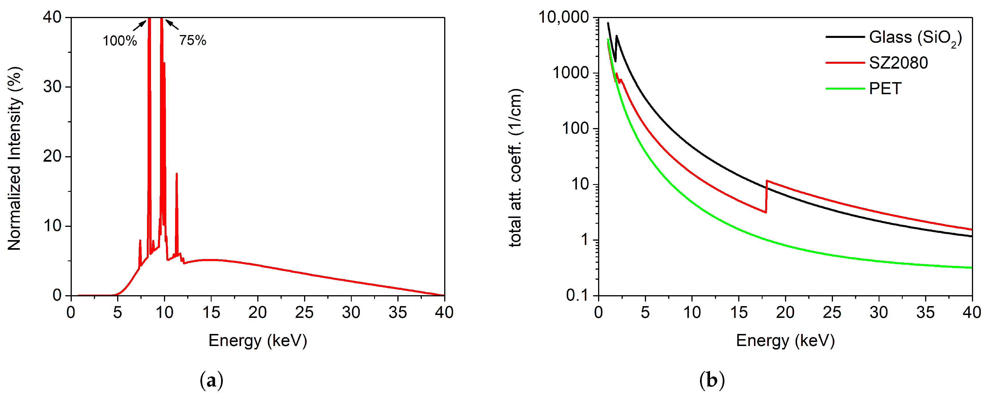
2.4. X-ray Computed Tomography (XCT) Setup

A ZEISS Xradia 620 Versa XCT device with a nominal basic spatial resolution of about 500 nm, when using the 40× optical magnification beamline [49], was employed. Scans of the DLW samples were acquired and reconstructed using the ZEISS Scout & Scan controller and reconstructor software (build version 16). A transmission tube (Nordson Dage Mark IV, Nordson DAGE, Aylesbury, UK) with a tungsten target and a nominal focal spot size of about 1.7 µm (full width half maximum, specified by the manufacturer) was utilised. Images were captured by an Andor CCD camera (iKon-L Series, Andor Technology, Belfast, UK) with 1024 × 1024 pixels at binning of two and a true physical pixel size of about 13.5 µm. Note that the achievable resolution of this setup is limited by the (unknown) scintillator thickness deposited at the used objective [26]. While rotating a sample at 360° within the X-ray beam path, a set of radiographic projections was taken at distinct angular positions. The set of projections served as input data for a 3D reconstruction [50]. The imaging device parameters are summarised in Table 2. A low tube voltage was used to achieve the highest resolution possible. Samples were scanned out-of-substrate-plane. For image analysis, we used the software Dragonfly Pro 2020.2 (Object Research Systems) and VG-Studio Max 3.4.5 (Volume Graphics), and for X-ray attenuation and spectrum simulation—the software aRTist 2.10.0 (BAM Berlin) [51] was used. The X-ray energy spectrum was calculated using the following parameters: a tungsten–diamond transmission target with a 2 µm thick tungsten layer on a 500 µm thick diamond layer, maximum photon energy of 40 kV, vacuum window, 10 mm air filter. Parameters for the X-ray attenuation properties of used materials can be found in the description of Figure 4. Note that because of the applied X-ray setup, X-ray attenuation contrast is expected, accompanied by partial phase contrast (edge enhancement) caused by the flat X-ray cone beam angle in this particular ZEISS device [26].

2.5. Scanning Electron Microscopy (SEM)

SEM imaging was performed using a Zeiss Evo MA10 with a SE detector at a working distance of 3 mm and acceleration voltages from 5 kV to 15 kV. Samples were coated with 15 nm Gold to ensure electric conductivity.

3. Results

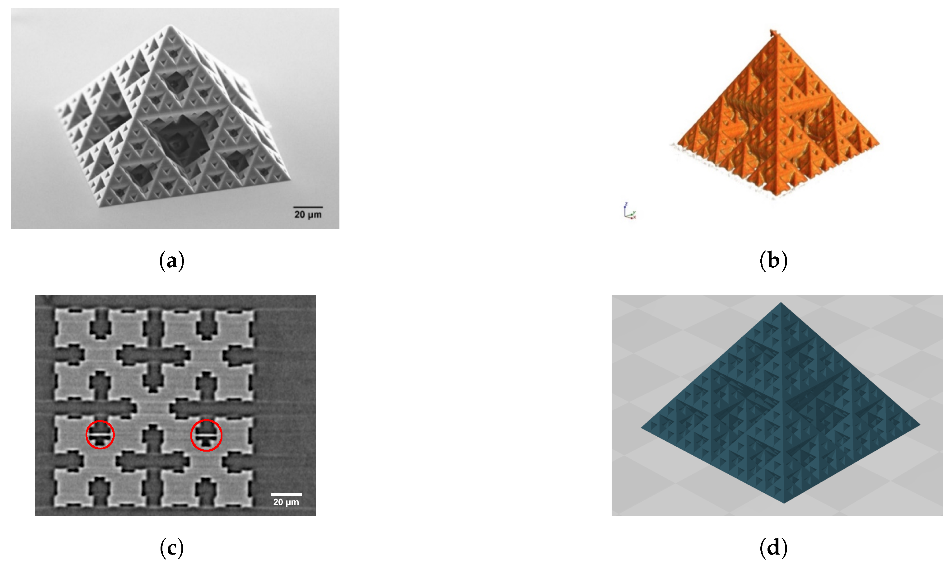
3.1. Fabrication Method—Practical Difficulties and Workflow Modifications

In previous works by Saha et al. [30], XRM structures were fabricated on a 750 µm pillar with the dip-in technology by Nanoscribe. With the SZ2080 photoresist, the dip-in method is not applicable. As SZ2080 must be baked [6] before the fabrication step, a preparation where a drop is casted on a small pillar, only very low structure heights would have been manufacturable as the drop height would be limited by the contact angle between pillar and photoresist. Thus, a conventional preparation technique on a flat substrate was preferred. Commonly, a glass substrate is used for DLW fabrication. However, glass and the deposited photoresist SZ2080 both intrinsically hold a very similar mass attenuation coefficient over the used X-ray energy spectrum, cf. Figure 4. In addition, the substrate and deposited polymer have very different sizes and material shadowing may occur here. To be precise, there are practical difficulties to image and align a big and flat (6 × 6 × 0.17 mm3) substrate with a small (0.141 × 0.141 × 0.1 mm3) sample on top in-plane along the X-ray beam path without any tilt.
Consequently, precession of the substrate that shadows the deposited structure over a wide range of the angular views may occur, cf. Figure 5. In general, for high-aspect-ratio samples, an out-of-plane alignment is preferred, as the substrate’s long side/thick edge passes the angular views only two times quickly. In an out-of-plane alignment, the pyramid’s top/bottom is imaged frontally and image information is maximised over a wide range of angular views. Note that the length of the X-ray beam path through the long side/thick edge is very large (up to 60 times larger) compared to the short side/thin edge and/or the pyramid’s size.
Glass is difficult to cut or break when considering the small size of the pyramid. It was not possible to prepare glass substrates with a side length smaller than 6 mm. To overcome these practical difficulties, the 170 µm glass substrate was substituted by a 0.17 mm PET foil with a much lower mass attenuation coefficient and density ρ , cf. Figure 4b. Moreover, samples are scanned out-of-plane, for which the substrate size was reduced to about 3 × 6 mm2. Thus, a longer X-ray travelling path through the substrate with a high aspect ratio was compensated by choosing a substrate with low attenuation coefficient and optimised sample alignment. In the PET–SZ2080 sample system, SZ2080 is a high absorbing material.
When exchanging the standard glass substrate by a PET-polymer substrate, a modification of the DLW fabrication process is needed, as illustrated in Figure 6. The mechanical properties of glass and polymer are very different. For instance, polymer easily bends under load of the optical system (oil and objective). The common DLW fabrication approach through the substrate, where oil is applied on top of the substrate and pre-baked SZ2080 is applied underneath (structure is built under the substrate), cannot be applied here. Instead of this, the immersion oil was directly applied on the pre-baked SZ2080 droplet on top of the PET-polymer substrate, and the structure was built “on top of the substrate”. Note that the PET-substrate was mechanically stabilised by another glass slide from the bottom. A disadvantage of this setup is that the immersion oil dissolves the photoresist at a slow rate of an estimated 0.01 mm/h and thus, fast fabrication is advised.

3.2. Evaluation of DLW Structures via XCT

Due to the complex environment and setup of the DLW process, a multitude of flaws of different origin can occur. Such flaws may include cracks, pores, unintended polymerised regions, damaged regions, shape deviations such as binding or bulging or a lack of surface adhesion. Imperfections most probably stem from the difficult sample handling and preparation, but also fabrication process related issues may occur, e.g., in the fabrication or development phase.
During the DLW process, the in situ observation possibilities are limited due to the simple visible light camera setup used. Unintended defects can have multiple origins and require a complete understanding of the DLW process to trace their original source. This includes software or hardware errors, as well. Therefore, non-destructive methods have to be used after the fabrication step in order to analyse the quality of the fabricated part and trace the orign of flaws.
An SEM image and corresponding XCT images of a fabricated fractal pyramid (sample 1) are shown in Figure 7a and Figure 7c, respectively. The lateral dimensions and geometry of the fractal pyramid could be resolved by XCT. Pores and cracks in the solid polymer region are not detected, but there were unintended polymerised regions, and small misalignments. The pyramid is slightly tilted and pressed into the substrate, which highlights the difficulties of using a bendable substrate (PET foil) and alignment within the DLW setup. (Note the video in the Appendix A that illustrates the tilt). Unintended polymerised regions, e.g., additional fabricated lines between the actual structure, are presumably caused by a bug in the slicing software. This line cannot be observed via SEM as it is hidden. We assume that those lines stem from the slicing algorithm itself as Cura sliced samples were fabricated without additional lines. They occur in one direction exclusively, e.g., the X-direction. One of those flaws is highlighted on a horizontal slice of the fractal pyramide in Figure 7c. Such lines are caused due to an error in either the STL (3D model data format) or the slicer or bad command interpretation from the DLW device. If such a flaw is hidden inside of a complex structure, it cannot be detected from the outside (SEM). Nevertheless, they may cause fundamental issues in the application of the structure, e.g., hinder the laminar flow in microfluidic applications. XCT or XRM testing is advised to detect such hidden flaws.
Radiographic testing methods become especially beneficial for DLW feedback of the produced parts quality when geometries with infill or intrinsic structures are produced. In the following, we want to investigate such a structure (sample 2) that was produced with a non-polymerised inner volume by using the Infill approach known from the FDM technique. Analogous to the FDM process, the inner volume of a structure does not have to be completely polymerised, but can be only partially converted by increasing the distance between the hatching lines. In Cura, a certain percantage of the inner volume can be left unchanged due to the reduction of written lines, and the total production time of structures is reduced significantly. Additional infill lines are then created by the slicer to strengthen the outer walls from collapse. The result is drastically reduced fabrication times. For instance, a bulk pyramid with a height of 100 µm and a side length of 141 µm and hatching and slicing distances of 200 nm has a fabrication time of 39 min 48 s. The same pyramid sliced with Cura and 8 outer walls and an infill line every 4 µm needs only 7 min 15 s to fabricate with a similar layer height of 200 nm. Thus, the fabrication time can be reduced by 81% by reducing the number of lines written in the structure. Therefore, it is highly desirable to use structures with an infill in DLW geometries applicable. Consequently, non-polymerised material is intended to be trapped inside the pyramid’s infill. However, multiple fabricated structures showed a missing tip of the pyramid.
Even though the same laser power and beam velocity was used for 3DPoli and Cura-sliced pyramids. XCT was utilised to investigate when the damage on the tip occurred, before or after the development of the sample. If the tip would have been broken off after the development of SZ2080, there should be material inside the pyramid. If the damage to the tip occurred before or while removing the pre-polymer, a clear density difference should be seen in the XCT between the infill structure (4 µm repeated pattern) and the removed photoresist. This is the case, as shown in Figure 8.
In Figure 8b, a horizontal and in Figure 8c, a vertical cross section of such a structure can be seen. The top of the fabricated pyramid shows a missing tip, see Figure 8d. The infill consists of individual lines (walls) that were produced as a single DLW-voxel line. Detection of internal (hidden) voxel-sized structures is possible to visualise with XCT. In addition to the missing tip, various internal defects were found by XCT (as highlighted in Figure 8b,c), for instance, bending of the infill and unintended polymerised regions. With the ability to individually slice an XCT-measured structure, the size and shape of such deformations can be quantified. We assume that the bending stems from the capillary forces that occurred during the development of the structure. The unintended polymerised region in the diagonal direction of the pyramid’s base stems from misinterpretations of the used slicing code. With further tuning of the fabrication parameters and decreasing the beam velocity, it was possible to obtain consistent results with entirely fabricated tips. This detailed XCT analysis demonstrates that not only the beam velocity and laser power play a role in successful fabrication, but also the slicing software. XCT proved to be a valuable analysis technique for DLW-fabricated structures. XCT was able to individually determine the origin of different flaws in the fabrication procedure by displaying them, which enables the operator to find an individual solution for the missing tip and the misinterpreted lines in the slicing code. Therefore, XCT is a highly useful tool for the process feedback of DLW-produced structures on the micro- and nanometer scale.

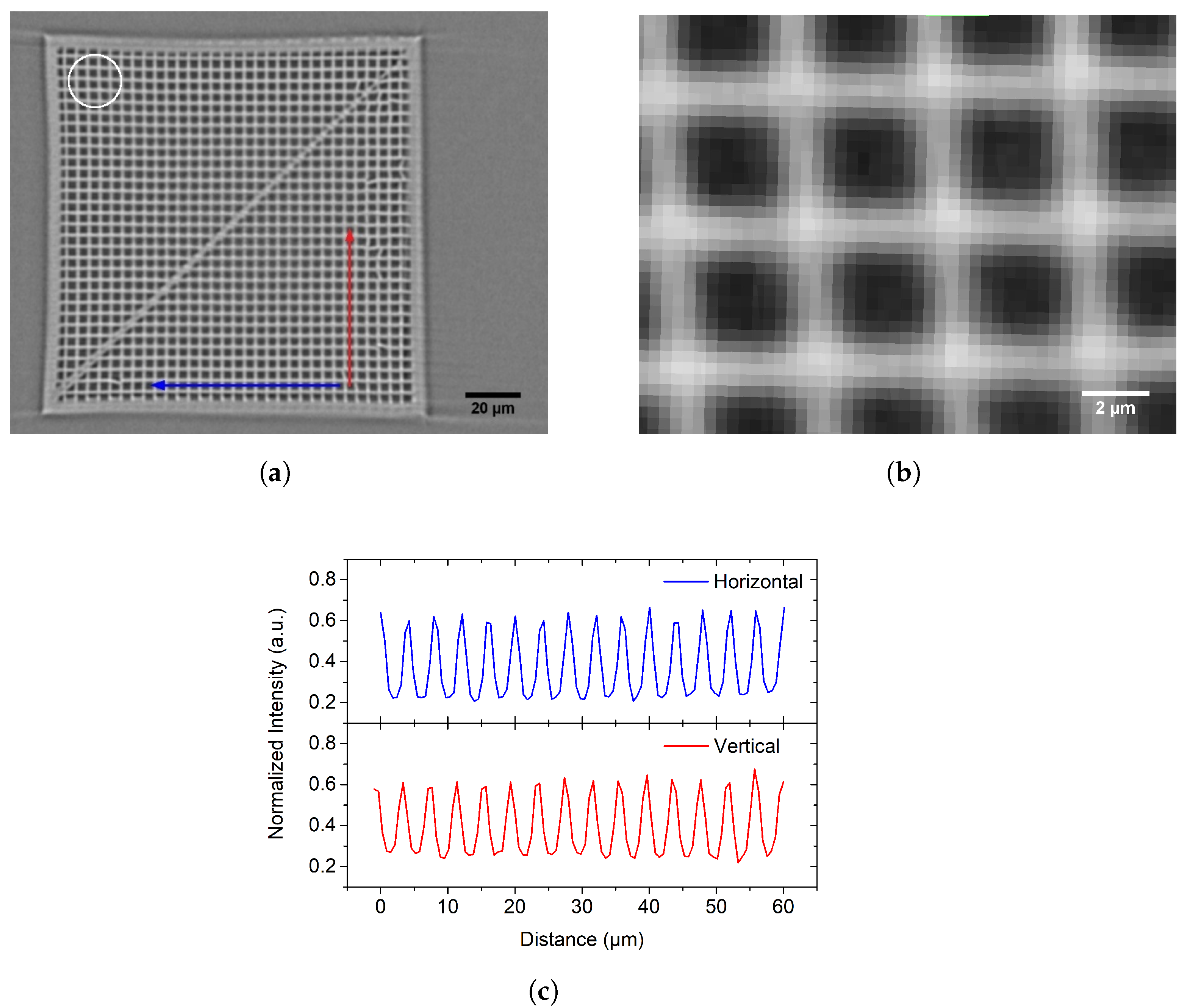
3.3. Resolution of XCT Measurements on DLW Structures

For sample 1, although the fractal pyramid’s recursive depth of four is clearly visible by the human eye in the 3D rendering of the XCT scan (cf. Figure 7a), it was not possible to find a reliable workflow to validate the exact sizes of the stacked pyramidal shapes in 3D. A strong X-ray phase contrast on the object’s surfaces, and the nested nature of the pyramidal shapes, hinder a clear determination of starting and end points for measurements. Direct length measurements and 3D volume measurements are influenced by artefacts and phase contrast, which are issues to be addressed in upcoming studies. However, the bulk four-sided pyramid (sample 2) with infill structures arranged in a checkerboard manner with a nominal cell repetition size of 4 µm (wall and cavity) are a suitable feature to be measured. When slicing parallel to the pyramid base, a mesh-like structure of the infill walls is visible (see Figure 8a), which serves as a repeatable measure in this structure. An intensity line profile was measured along the mesh-cells, as indicated by the red and blue arrows in Figure 9a and plotted in Figure 9b. By calculating the turning points of the line profile slope from the peaks of the first derivative, an average cell repetition size of blue cells c r b l u e = 4.00 ± 0.08 µm and red cells c r r e d = 4.03 ± 0.1 µm could be shown. The cell size is measured as a distance in between turning points corresponding to the start of a mesh-solid/end of a mesh-cavity and start of a mesh-cavity/end of a mesh-solid. A single mesh-solid line shows an average thickness of about s b l u e = 1.51 ± 0.06 µm and s r e d = 1.57 ± 0.06 µm, whereas the mesh-cavities have an average thickness of about l b l u e = 2.49 ± 0.08 µm and l r e d = 2.47 ± 0.07 µm. However, the true sizes of the pyramid’s internal features are unknown, but the “coarse” cell repetition size of about 4 µm matches the nominal input parameters of the slicer very well.
The present reference phantom designs and XCT scanning setup are not optimal yet. However, the aim of the study is to highlight the synergies (and challenges) in between DLW and XCT/XRM (at their resolution limits). Detailed studies which focus on the nano fabrication of trustable and repeatable structure sizes are needed. Additionally, experiments utilizing an XRM with a basic spatial resolution up to 50 nm are emphasised.
For future reference structures (phantoms) in the field of XCT/XRM, the proposed DLW-fabricated structures are generally suitable. The fractal pyramid shows self-similar geometries that decrease in size per recursive step and intuitively demonstrate the XCT/XRM resolution limit in 3D when the recursive step size is pushed to its limits. The measurement of hidden, mesh-like walls within the second pyramid naturally illustrates the superiority of the non-destructive XCT/XRM 3D imaging technique in this aspect over SEM or light microscopy very clearly. For demonstrations of the XCT/XRM smallest feature detectability and DLW-producibility near the absolute resolution limit of DLW/XCT/XRM, future studies need to focus on more systematic investigations of simple phantom designs with feature sizes scaling towards the DLW single voxel line of a certain/constant (optimal) DLW device parameter set. To use such DLW structures as commercial reference objects, reproducibility is the major concern. Moreover, the precision of the fabricated sizes would need to be checked twice, once by another method with much higher basic spatial resolution, e.g., SEM. Therefore, the correlative investigations of non-hidden features via SEM and XCT/XRM should be focused on as well. Although pyramidal geometries are proposed in this work, the design of phantoms is not limited to pyramidal shapes, and virtually any geometry can be produced by DLW. By choosing a geometrical reference XCT phantom design, it is possible to address different fields of application, for instance, the system resolution, contrast or signal-to-noise ratio, and imaging artefacts. Another test geometry that exploits the benefits of 3D additive manufacturing, is a nested hollow spheres arrangement with defined perforated surfaces, whereby sphere and hole diameters gradually reflect defined sizes from several tens of micrometers to hundreds of nanometers. Thus, the DLW method enables the general availability of 3D phantoms with complex testing patterns and bridges two length scales from micro- to nanometers, which is ideal for XCT/XRM resolution limit test phantoms.

4. Conclusions

Measurements of DLW structures with XCT/XRM have been a less studied field although both methods can clearly enrich each other. In this study, we have shown two similar sample geometries, including one where the XCT was used to analyse for hidden faults, which stem from the DLW fabrication process. It was demonstrated that XCT can identify sub-micron DLW-fabricated structures sufficiently, and thereby, can act as a feedback tool. Internal, hidden structures (fabrication flaws) could be observed, which are not detectable by other techniques such as SEM because of the 3D nature of the complex printed object. At sample 2, we could determine the time at which the structural fault occured. Additionally, sample 2 was used to determine the XCTs resolution along the fabricated infill lines. Thus, we could gather additional information by XCT that helped to verify the hypothesis on the origin of certain imperfections, and act accordingly, adjusting the DLW printing parameters. By using infills and Cura software, it was possible to reduce the total production time of a solid pyramid by 81%. XCT was essential to fine-tune the fabrication parameters. However, an adjustment of the DLW sample preparation route was needed for XCT imaging, in particular, by picking a PET-polymer substrate and a modified DLW process. The shown fabrication route on a PET substrate resulted in a stable process with a high contrast in the XCT compared to the previously used glass substrates. Therefore, XCT is a valuable tool in the quality assurance of DLW structures. Future imaging applications (XCT) for DLW may include studies on the residue of photoresist in microchannels or an internal analysis of microrobotic structures. Finally, we have reflected the usage of the shown structure for XCT phantoms. However, additional studies are needed for a robust and reproducable manufacturing of said phantoms.

Author Contributions

Conceptualization, S.F. and A.F.; methodology, S.F.; software, S.F. and A.F.; validation, S.F., A.F., L.P. and G.-R.J.; resources, S.F.; data curation, S.F.; writing—original draft preparation, S.F.; writing—review and editing, S.F. and A.F. All authors have read and agreed to the published version of the manuscript.

Funding

This research received no external funding.

Institutional Review Board Statement

Not applicable.

Informed Consent Statement

Not applicable.

Data Availability Statement

The data presented in this study are available on request from the corresponding author.

Conflicts of Interest

The authors declare no conflict of interest.

Appendix A

Chemical Composition of SZ2080

The name of SZ2080 is given by weight percentages of 20% inorganic (Zr, Si) and 80% organic elements. The molar ratio of methacryloxypropyl trimethoxysilane (MAPTMS) to zirconium propoxide (ZPO) is 8:2 [52]. Therefore, a proportion of Zr:Si 1 to 4 for the inorganic elements is given and the following sum formula can be obtained: C 36 H 68 O 20 S i 4 Z r The forumla is given in Figure A1.
Figure A1. Simplified formula of SZ2080 for a MAPTMS:ZPO ratio of 8:2, the order of the monomers is for illustration purposes.
Applsci 12 10488 g0a1

References

  1. Malinauskas, M.; Žukauskas, A.; Hasegawa, S.; Hayasaki, Y.; Mizeikis, V.; Buividas, R.; Juodkazis, S. Ultrafast laser processing of materials: From science to industry. Light. Sci. Appl. 2016, 5, e16133. [Google Scholar] [CrossRef] [PubMed] [Green Version]
  2. Skliutas, E.; Lebedevaite, M.; Kabouraki, E.; Baldacchini, T.; Ostrauskaite, J.; Vamvakaki, M.; Farsari, M.; Juodkazis, S.; Malinauskas, M. Polymerization mechanisms initiated by spatio-temporally confined light. Nanophotonics 2021, 10, 1211–1242. [Google Scholar] [CrossRef]
  3. Cao, Y.; Gan, Z.; Jia, B.; Evans, R.A.; Gu, M. High-photosensitive resin for super-resolution direct-laser-writing based on photoinhibited polymerization. Opt. Express 2011, 19, 19486–19494. [Google Scholar] [CrossRef] [PubMed]
  4. Burmeister, F.; Steenhusen, S.; Houbertz, R.; Zeitner, U.D.; Nolte, S.; Tünnermann, A. Materials and technologies for fabrication of three-dimensional microstructures with sub-100 nm feature sizes by two-photon polymerization. J. Laser Appl. 2012, 24, 042014. [Google Scholar] [CrossRef] [Green Version]
  5. Houbertz, R.; Domann, G.; Cronauer, C.; Schmitt, A.; Martin, H.; Park, J.U.; Fröhlich, L.; Buestrich, R.; Popall, M.; Streppel, U.; et al. Inorganic–organic hybrid materials for application in optical devices. Thin Solid Film. 2003, 442, 194–200. [Google Scholar] [CrossRef]
  6. Ovsianikov, A.; Viertl, J.; Chichkov, B.; Oubaha, M.; MacCraith, B.; Sakellari, I.; Giakoumaki, A.; Gray, D.; Vamvakaki, M.; Farsari, M.; et al. Ultra-low shrinkage hybrid photosensitive material for two-photon polymerization microfabrication. ACS Nano 2008, 2, 2257–2262. [Google Scholar] [CrossRef]
  7. Ovsianikov, A.; Shizhou, X.; Farsari, M.; Vamvakaki, M.; Fotakis, C.; Chichkov, B.N. Shrinkage of microstructures produced by two-photon polymerization of Zr-based hybrid photosensitive materials. Opt. Express 2009, 17, 2143–2148. [Google Scholar] [CrossRef]
  8. Jonušauskas, L.; Gailevičius, D.; Mikoliūnaitė, L.; Sakalauskas, D.; Šakirzanovas, S.; Juodkazis, S.; Malinauskas, M. Optically clear and resilient free-form μ-optics 3D-printed via ultrafast laser lithography. Materials 2017, 10, 12. [Google Scholar] [CrossRef] [Green Version]
  9. Gissibl, T.; Thiele, S.; Herkommer, A.; Giessen, H. Two-photon direct laser writing of ultracompact multi-lens objectives. Nat. Photonics 2016, 10, 554–560. [Google Scholar] [CrossRef]
  10. Guo, R.; Xiao, S.; Zhai, X.; Li, J.; Xia, A.; Huang, W. Micro lens fabrication by means of femtosecond two photon photopolymerization. Opt. Express 2006, 14, 810–816. [Google Scholar] [CrossRef]
  11. Stankevičius, E.; Malinauskas, M.; Račiukaitis, G. Fabrication of scaffolds and micro-lenses array in a negative photopolymer SZ2080 by multi-photon polymerization and four-femtosecond-beam interference. Phys. Procedia 2011, 12, 82–88. [Google Scholar] [CrossRef] [Green Version]
  12. Bieda, M.; Bouchard, F.; Lasagni, A.F. Two-photon polymerization of a branched hollow fiber structure with predefined circular pores. J. Photochem. Photobiol. A Chem. 2016, 319, 1–7. [Google Scholar] [CrossRef]
  13. Vanderpoorten, O.; Peter, Q.; Challa, P.K.; Keyser, U.F.; Baumberg, J.; Kaminski, C.F.; Knowles, T.P. Scalable integration of nano-, and microfluidics with hybrid two-photon lithography. Microsyst. Nanoeng. 2019, 5, 40. [Google Scholar] [CrossRef] [Green Version]
  14. Mačiulaitis, J.; Deveikytė, M.; Rekštytė, S.; Bratchikov, M.; Darinskas, A.; Šimbelytė, A.; Daunoras, G.; Laurinavičienė, A.; Laurinavičius, A.; Gudas, R.; et al. Preclinical study of SZ2080 material 3D microstructured scaffolds for cartilage tissue engineering made by femtosecond direct laser writing lithography. Biofabrication 2015, 7, 015015. [Google Scholar] [CrossRef]
  15. Shpichka, A.; Koroleva, A.; Kuznetsova, D.; Burdukovskii, V.; Chichkov, B.; Bagratashvili, V.; Timashev, P. Two-photon polymerization in tissue engineering. In Polymer and Photonic Materials towards Biomedical Breakthroughs; Springer: Berlin/Heidelberg, Germany, 2018; pp. 71–98. [Google Scholar]
  16. Pertoldi, L.; Zega, V.; Comi, C.; Osellame, R. Dynamic mechanical characterization of two-photon-polymerized SZ2080 photoresist. J. Appl. Phys. 2020, 128, 175102. [Google Scholar] [CrossRef]
  17. Butkutė, A.; Čekanavičius, L.; Rimšelis, G.; Gailevičius, D.; Mizeikis, V.; Melninkaitis, A.; Baldacchini, T.; Jonušauskas, L.; Malinauskas, M. Optical damage thresholds of microstructures made by laser three-dimensional nanolithography. Opt. Lett. 2020, 45, 13–16. [Google Scholar] [CrossRef]
  18. Žukauskas, A.; Batavičiūtė, G.; Ščiuka, M.; Jukna, T.; Melninkaitis, A.; Malinauskas, M. Characterization of photopolymers used in laser 3D micro/nanolithography by means of laser-induced damage threshold (LIDT). Opt. Mater. Express 2014, 4, 1601–1616. [Google Scholar] [CrossRef]
  19. Žukauskas, A.; Matulaitienė, I.; Paipulas, D.; Niaura, G.; Malinauskas, M.; Gadonas, R. Tuning the refractive index in 3D direct laser writing lithography: Towards GRIN microoptics. Laser Photonics Rev. 2015, 9, 706–712. [Google Scholar] [CrossRef]
  20. LaFratta, C.N.; Baldacchini, T. Two-photon polymerization metrology: Characterization methods of mechanisms and microstructures. Micromachines 2017, 8, 101. [Google Scholar] [CrossRef] [Green Version]
  21. Suzuki, T.; Morikawa, J.; Hashimoto, T.; Buividas, R.; Gervinskas, G.; Paipulas, D.; Malinauskas, M.; Mizeikis, V.; Juodkazis, S. Thermal and optical properties of sol-gel and SU-8 resists. In Proceedings of the Advanced Fabrication Technologies for Micro/Nano Optics and Photonics V, SPIE, San Francisco, CA, USA, 21–26 January 2012; Volume 8249, pp. 93–101. [Google Scholar]
  22. Cnudde, V.; Boone, M.N. High-resolution X-ray computed tomography in geosciences: A review of the current technology and applications. Earth-Sci. Rev. 2013, 123, 1–17. [Google Scholar] [CrossRef]
  23. Holt, M.; Harder, R.; Winarski, R.; Rose, V. Nanoscale hard X-ray microscopy methods for materials studies. Annu. Rev. Mater. Res. 2013, 43, 183–211. [Google Scholar] [CrossRef]
  24. Lider, V.V. X-ray microscopy. Uspekhi Fiz. Nauk 2017, 187, 201–219. [Google Scholar] [CrossRef]
  25. Ewert, U.; Zscherpel, U.; Heyne, K.; Jechow, M.; Bavendiek, K. Image Quality in Digital Industrial Radiography. Mater. Eval. 2012, 70, 955–964. [Google Scholar]
  26. Zabler, S.; Ullherr, M.; Fella, C.; Schielein, R.; Focke, O.; Zeller-Plumhoff, B.; Lhuissier, P.; DeBoever, W.; Hanke, R. Comparing image quality in phase contrast subμ X-ray tomography—A round-robin study. Nucl. Instruments Methods Phys. Res. Sect. A Accel. Spectrometers Detect. Assoc. Equip. 2020, 951, 162992. [Google Scholar] [CrossRef] [Green Version]
  27. Sarapata, A.; Ruiz-Yaniz, M.; Zanette, I.; Rack, A.; Pfeiffer, F.; Herzen, J. Multi-contrast 3D X-ray imaging of porous and composite materials. Appl. Phys. Lett. 2015, 106, 154102. [Google Scholar] [CrossRef]
  28. Davis, G.R.; Elliott, J.C. Artefacts in X-ray microtomography of materials. Mater. Sci. Technol. 2006, 22, 1011–1018. [Google Scholar] [CrossRef]
  29. Saha, S.K.; Divin, C.; Cuadra, J.A.; Panas, R.M. Effect of proximity of features on the damage threshold during submicron additive manufacturing via two-photon polymerization. J. Micro Nano-Manuf. 2017, 5, 031002. [Google Scholar] [CrossRef] [Green Version]
  30. Saha, S.K.; Oakdale, J.S.; Cuadra, J.A.; Divin, C.; Ye, J.; Forien, J.B.; Bayu Aji, L.B.; Biener, J.; Smith, W.L. Radiopaque resists for two-photon lithography to enable submicron 3D imaging of polymer parts via X-ray computed tomography. ACS Appl. Mater. Interfaces 2018, 10, 1164–1172. [Google Scholar] [CrossRef] [PubMed]
  31. Tičkūnas, T.; Paipulas, D.; Purlys, V. Dynamic voxel size tuning for direct laser writing. Opt. Mater. Express 2020, 10, 1432–1439. [Google Scholar] [CrossRef]
  32. Pandey, P.M.; Reddy, N.V.; Dhande, S.G. Slicing procedures in layered manufacturing: A review. Rapid Prototyp. J. 2003, 9, 274–288. [Google Scholar] [CrossRef] [Green Version]
  33. Qamar Tanveer, M.; Mishra, G.; Mishra, S.; Sharma, R. Effect of infill pattern and infill density on mechanical behaviour of FDM 3D printed Parts- a current review. Mater. Today Proc. 2022, 62, 100–108. [Google Scholar] [CrossRef]
  34. Micro-CT Bar Pattern Phantoms—A PTW Company. QRM Quality Assurance in Radiology and Medicine GmbH. Available online: https://www.qrm.de/en/products/micro-ct-bar-pattern-phantoms/ (accessed on 10 August 2022).
  35. Aletheia Spatial Targets. Available online: http://www.aletheia-imaging.com/ (accessed on 22 September 2022).
  36. Rueckel, J.; Stockmar, M.; Pfeiffer, F.; Herzen, J. Spatial resolution characterization of a X-ray microCT system. Appl. Radiat. Isot. 2014, 94, 230–234. [Google Scholar] [CrossRef]
  37. Blažek, P.; Šrámek, J.; Zikmund, T.; Kalasová, D.; Hortvík, V.; Klapetek, P.; Kaiser, J. Voxel size and calibration for CT measurements with a small field of view. In Proceedings of the 9th Conference on Industrial Computed Tomography (iCT 2019), Padova, Italy, 13–15 February 2019. [Google Scholar]
  38. ASTM E1441-19; Guide for Computed Tomography (CT) Imaging. ASTM International: West Conshohocken, PA, USA, 2019.
  39. ASTM E1695-20E1; Standard Test Method for Measurement of Computed Tomography (CT) System Performance. ASTM International: West Conshohocken, PA, USA, 2020.
  40. ASTM E1935-97R19; Standard Test Method for Calibrating and Measuring (CT) Density. ASTM International: West Conshohocken, PA, USA, 2019.
  41. ISO 15708; Non-Destructive Testing—Radiation Methods for Computed Tomography. International Organization for Standardization: Geneva, Switzerland, 2017.
  42. de Oliveira, M.V.; Wenzel, A.; Campos, P.S.; Spin-Neto, R. Quality assurance phantoms for cone beam computed tomography: A systematic literature review. Dentomaxillofac. Radiol. 2017, 46, 20160329. [Google Scholar] [CrossRef] [Green Version]
  43. Silva, W.; Zscherpel, U.; Ewert, U.; Lopes, R. Analysis of angular dependent spatial frequency response of Digital Coplanar Translational Laminography. NDT E Int. 2021, 124, 102546. [Google Scholar] [CrossRef]
  44. Gach, H.M.; Tanase, C.; Boada, F. 2D & 3D Shepp-Logan phantom standards for MRI. In Proceedings of the 2008 19th International Conference on Systems Engineering, Las Vegas, NV, USA, 19–21 August 2008; pp. 521–526. [Google Scholar]
  45. Du, L.Y.; Umoh, J.; Nikolov, H.N.; Pollmann, S.I.; Lee, T.Y.; Holdsworth, D.W. A quality assurance phantom for the performance evaluation of volumetric micro-CT systems. Phys. Med. Biol. 2007, 52, 7087–7108. [Google Scholar] [CrossRef]
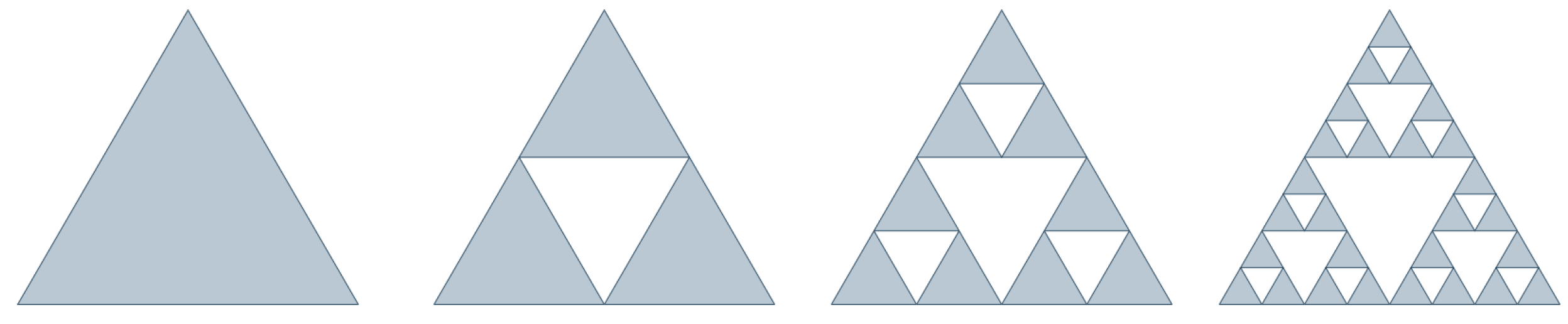
  46. Sierpinski, W. Sur une courbe dont tout point est un point de ramification. CR Acad. Sci. 1915, 160, 302–305. [Google Scholar]
  47. Barnsley, M.F.; Hutchinson, J.E.; Stenflo, Ö. V-variable fractals: Fractals with partial self similarity. Adv. Math. 2008, 218, 2051–2088. [Google Scholar] [CrossRef] [Green Version]
  48. Zeitler, H. Tetrahedron and octahedron fractals. Int. J. Math. Educ. Sci. Technol. 1998, 29, 329–341. [Google Scholar] [CrossRef]
  49. Web Page of Xradia 610/620 Versa-Series. Available online: https://www.zeiss.com/microscopy/int/products/x-ray-microscopy/zeiss-xradia-610-and-620-versa.html (accessed on 16 October 2022).
  50. Feldkamp, L.A.; Davis, L.C.; Kress, J.W. Practical cone-beam algorithm. Josa A 1984, 1, 612–619. [Google Scholar] [CrossRef] [Green Version]
  51. aRTist—Analytical RT Inspection Simulation Tool—artist.bam.de. Available online: http://artist.bam.de/ (accessed on 25 August 2022).
  52. Giakoumaki, A.N.; Kenanakis, G.; Klini, A.; Androulidaki, M.; Viskadourakis, Z.; Farsari, M.; Selimis, A. 3D micro-structured arrays of ZnO nanorods. Sci. Rep. 2017, 7, 2100. [Google Scholar] [CrossRef]
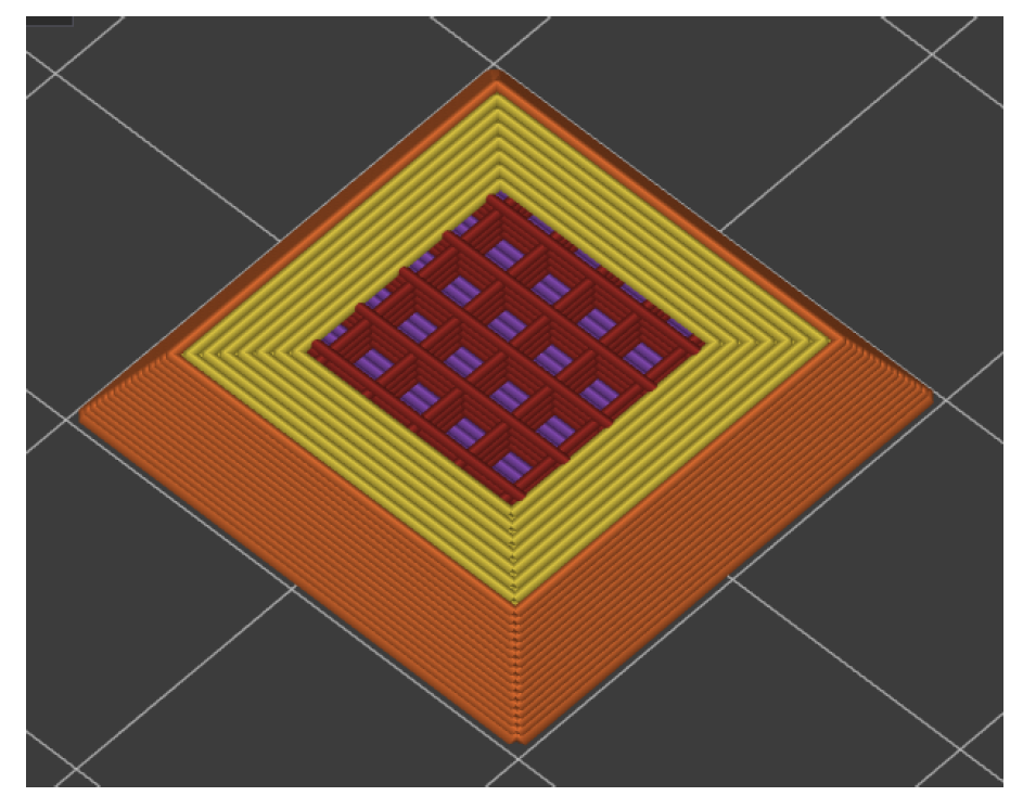
Figure 1. Illustration of a fractal triangle in 2D with increasing recursive depth of 0 to 3 (left to right).
Applsci 12 10488 g001
Figure 2. Partial Fractal octahedron structure (as used in sample 1) cut along the X and Y-plane for illustration purposes to highlight the complex inner structure; the shown object was manufactured via Fused Deposition Modelling.
Applsci 12 10488 g002
Figure 3. Exemplary illustration of a slice through the tool paths and naming conventions for sample 2 shown in PrusaSlicer software, 8 outer walls in red/orange for the outermost wall, purple for the solid bottom layer and red the hatched infill every 4 µm. The shown sliced pyramid is scaled by a fourth.
Applsci 12 10488 g003
Figure 4. (a) X-ray spectrum of the used setup calculated with aRTist (parameters see Section 2.4). Note that most photons are created in the low-energy range around 10 kV (characteristic lines of tungsten) and at the mean energy of the bremsstrahlung at around 15 kV. (b) Total linear attenuation coefficients of glass (SiO2, ρ S i = 2.2 g · cm 3 ), SZ2080 (C36H68O20Si4Zr, ρ S Z 2080 = 1.2 g · cm 3 ) and PET (C10H8O4, ρ P E T = 1.38 g · cm 3 ).
Applsci 12 10488 g004
Figure 5. Illustration of shadowing of structure by glass substrate.
Applsci 12 10488 g005
Figure 6. Different examined process possibilities to fabricate a structure via DLW, left to right: Through a glass substrate (standard route), through a thin polymer foil (tested, but no structures observed) and on top of polymer foil (applied route in this study).
Applsci 12 10488 g006
Figure 7. Views of a DLW fabricated fractal pyramid (sample 1): (a) SEM image, (b) 3D rendering from XCT and (c) XCT slice view parallel to the Z-plane (perpendicular to the building direction). Unintended polymerised lines are highlighted in (c). A 3D rendering of the binary STL-file is shown in (d).
Applsci 12 10488 g007
Figure 8. A SEM image of a bulk pyramid (sample 2) with complete fabricated tip is shown in (a). XCT images of a sample 2 variant with missing tip is shown in: (b) horizontal (X-plane) and (c) vertical (Z-plane) XCT view with highlighted defects (red arrows), and (d) as a 3D rendering (clipped).
Applsci 12 10488 g008
Figure 9. (a) Horizontal slice through the structure, the blue and red arrows mark a line measurement; (b) Zoom-in of high-resolution image area corresponding to the white circle in (a). Square-like areas of the same gray value correspond to a cut of a voxel with a nominal size of 0.33 × 0.33 × 0.33 µm3. (Voxels appear in a non-regular grid, as the original voxel grid of the scan and virtual grid of the scanned object do not match. The sample was slightly tilted during the scan. However, the image was aligned to the object’s grid, therefore, the voxel grid appears to be tilted in the print-out); (c) Normalised intensity along the blue and red arrow shows clear detectability of multiple single voxel walls.
Applsci 12 10488 g009
Table 1. Summary of the two sample geometries.
SampleTypeHeight; Side Length (µm)SlicerSlicer Options
1Fractal Pyramid141; 1003DPoliHatching and Slicing distance = 200 nm
2Full Pyramid141; 100Cura8 outer walls, single infill line every 4 µm
Table 2. Summary of XCT imaging parameters, including source–object distance (SOD), object–detector distance (ODD), geometrical magnification (Mgeo), optical magnification (Mopt), exposure time (texp), effective pixel size (PSeff) and number of projections (Nproj).
Voltage (kV)Power (W)FilterSOD (mm)ODD (mm)MgeoMopttexp (s)PSeff (µm)Nproj
403None10102x40x140.33801
Publisher’s Note: MDPI stays neutral with regard to jurisdictional claims in published maps and institutional affiliations.

