
Microwave SINIS Detectors

 , , ,
, , ,
Abstract
:Featured Application
Abstract
1. Introduction
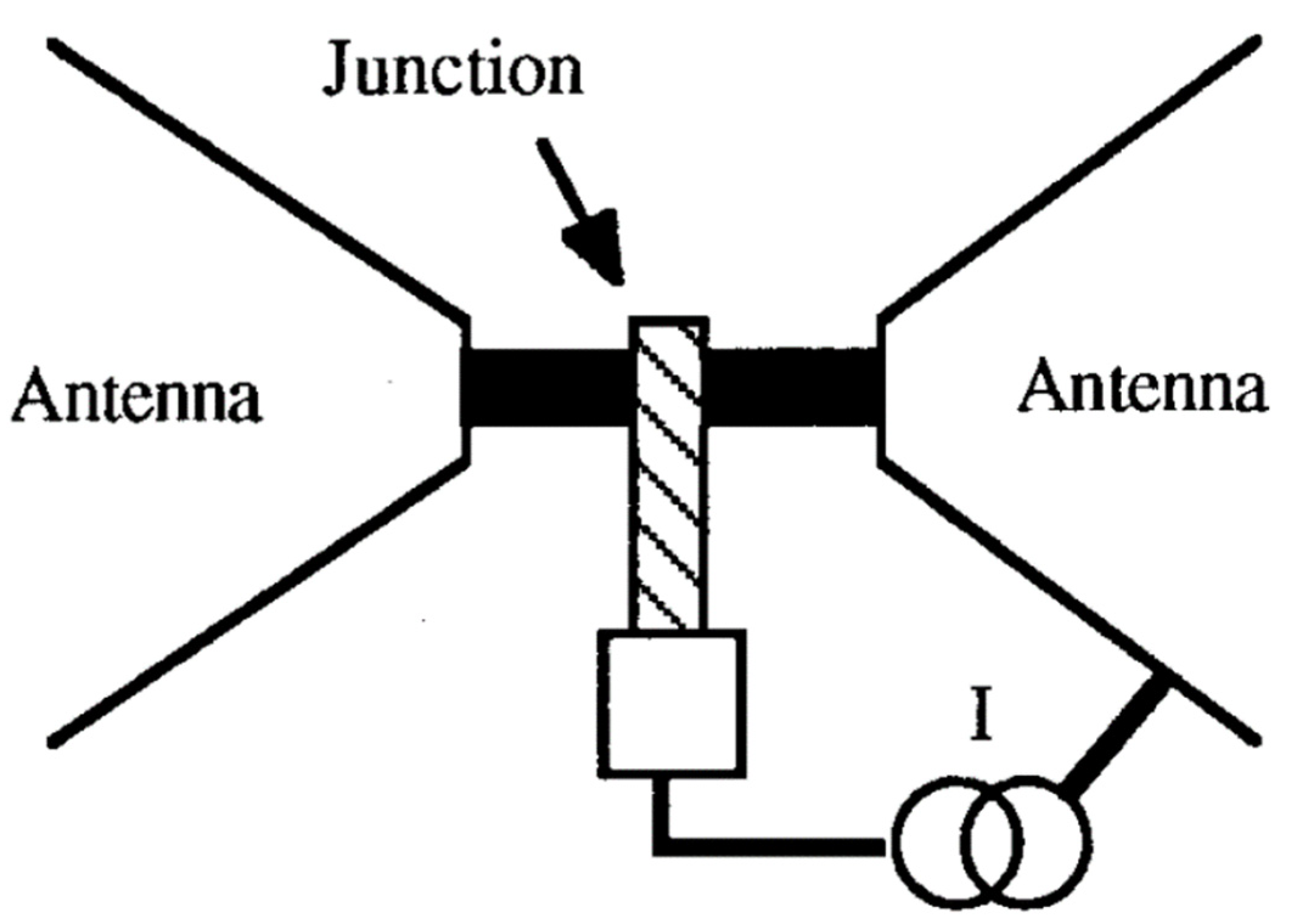
2. Electron Cooling
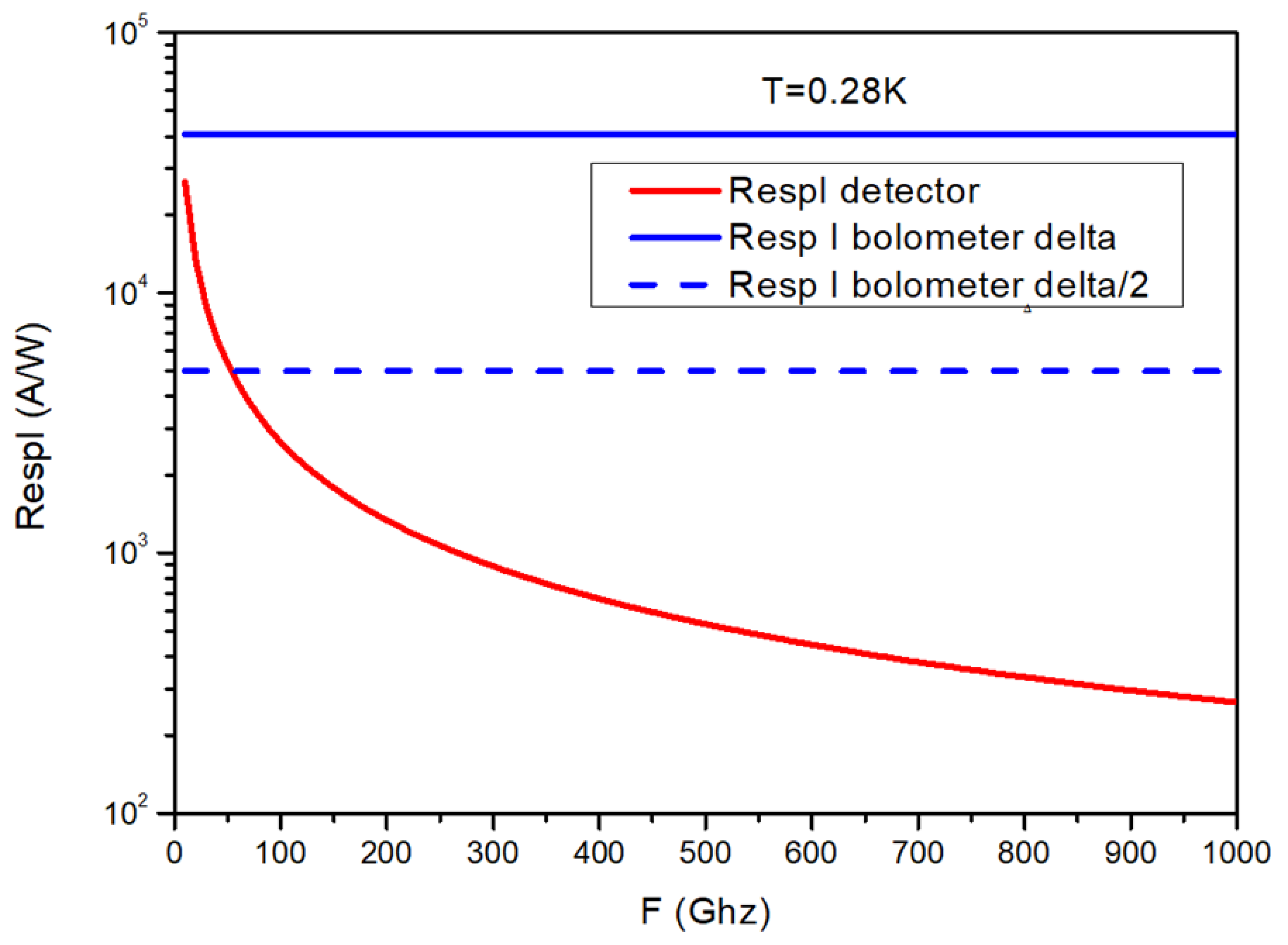
3. Quantum and Bolometric Response
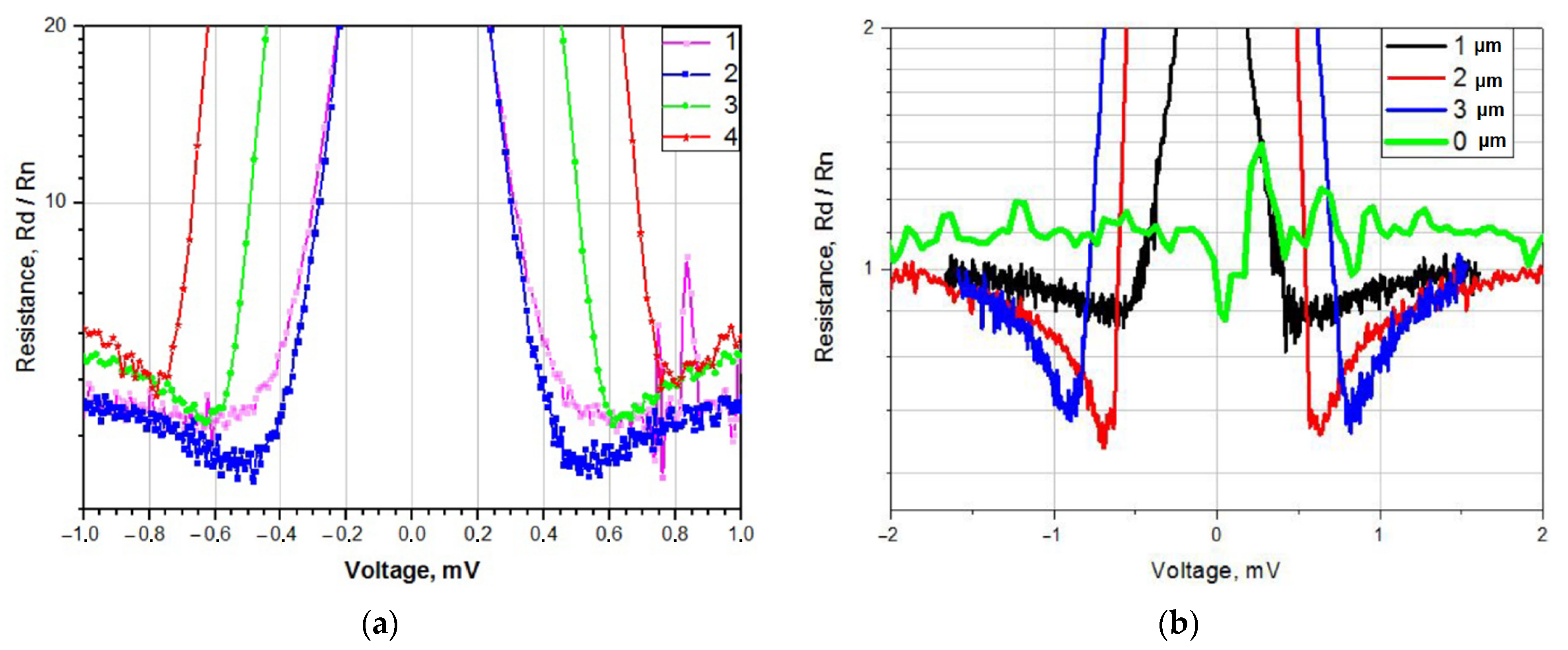
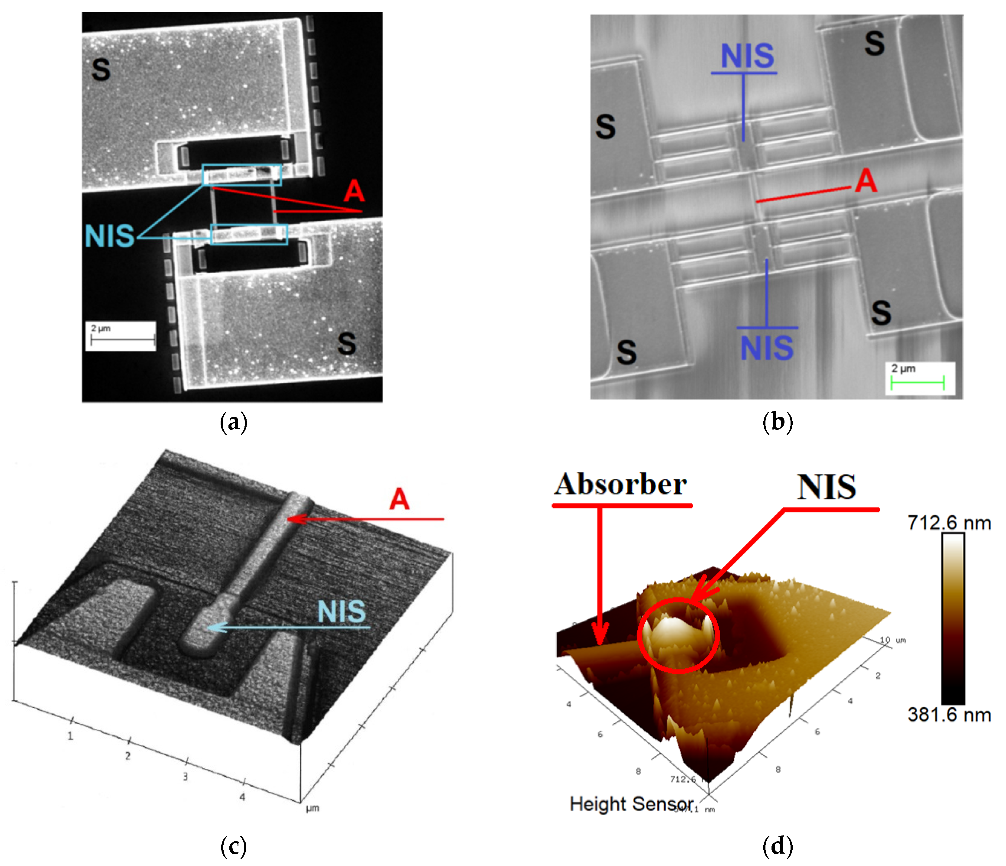
4. Traps for Hot Quasiparticles in a Superconductor
- (1)
- Superconducting electrodes deposited above the trilayer Ti/Au/Pd normal metal electrodes (distance to the normal metal trap is 2 μm);
- (2)
- Layout similar to the first, but superconducting electrodes are placed on thin Ti/Pd. In both cases, the ratio of superconducting aluminum to the area of the NIS junction is SAl/SSIN = 3;
- (3)
- The area of the superconducting electrode is much larger, and the superconductor is placed above the normal Ti/Pd, but the distance from the NIS to the normal electrodes is the same as in the previous two;
- (4)
- The area of superconducting electrodes is increased further (SAl/SSIN = 200), and the distance from NIS junctions to normal electrodes is increased to 5 μm.
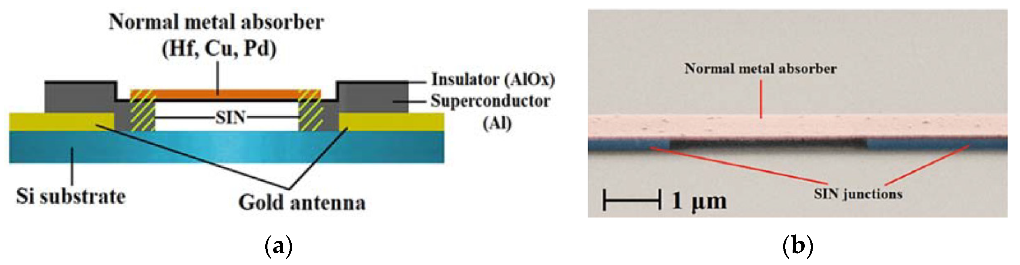
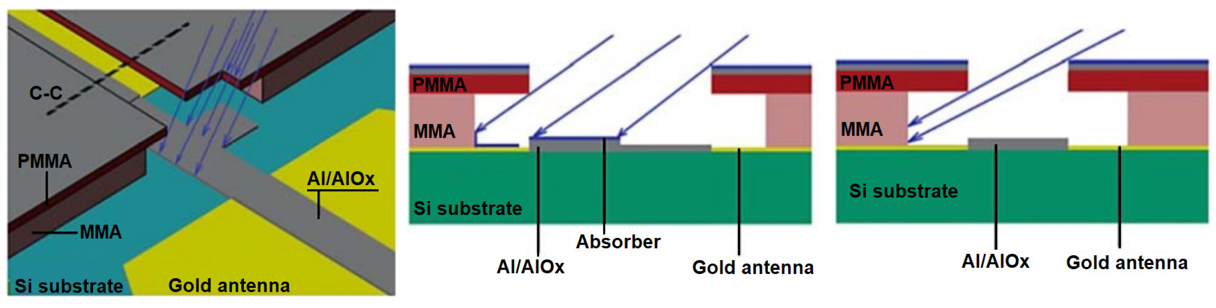
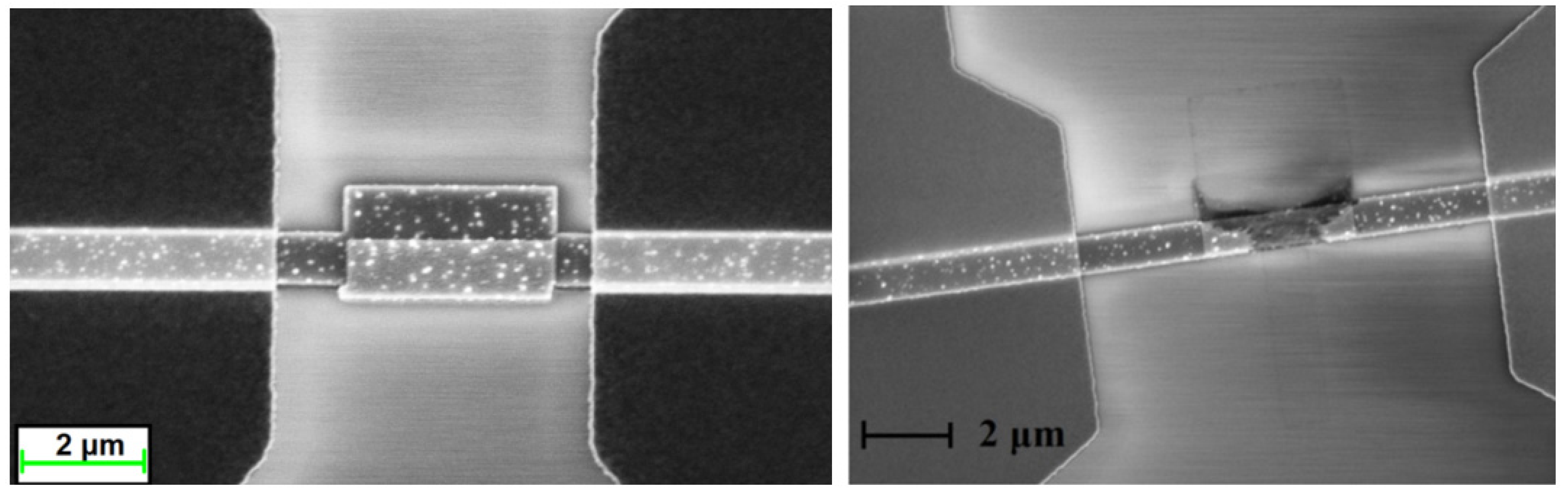
5. Fabrication Technology of SINIS
5.1. Shadow Evaporation Technology
5.2. Direct Deposition Technology
5.3. Fabrication of SINIS Junctions with Suspended Absorber
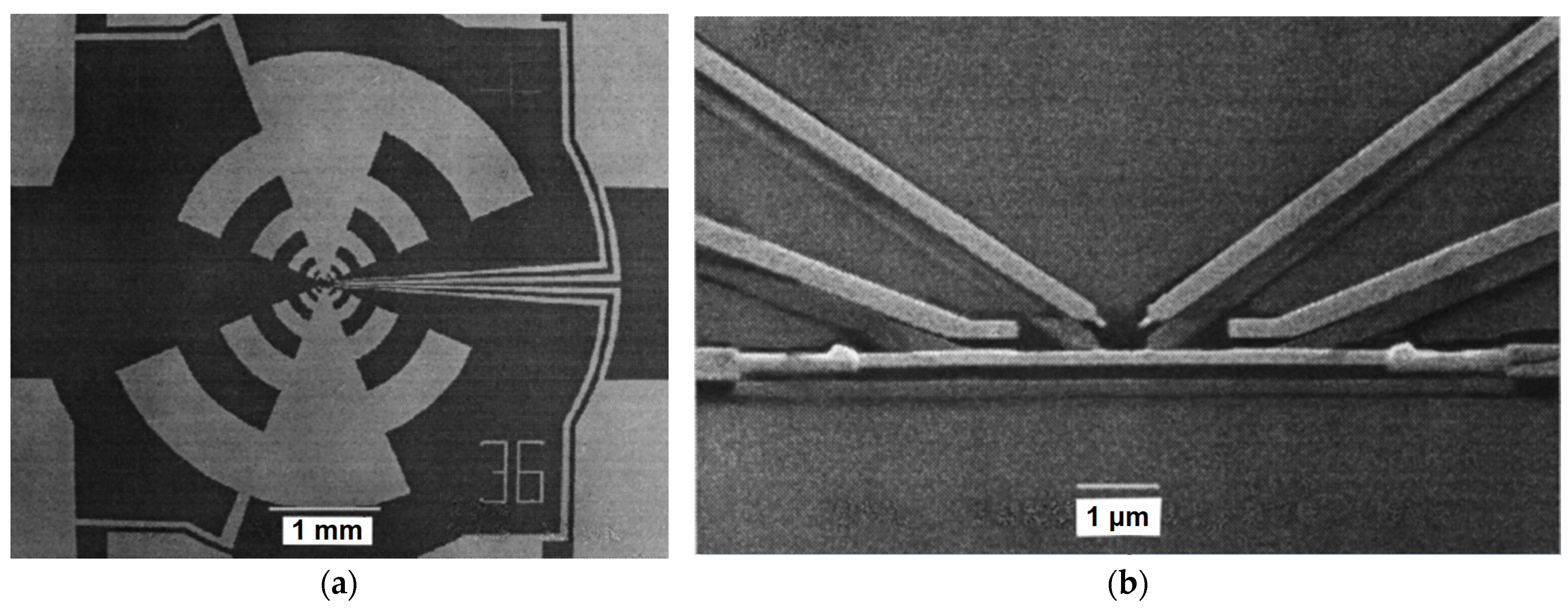
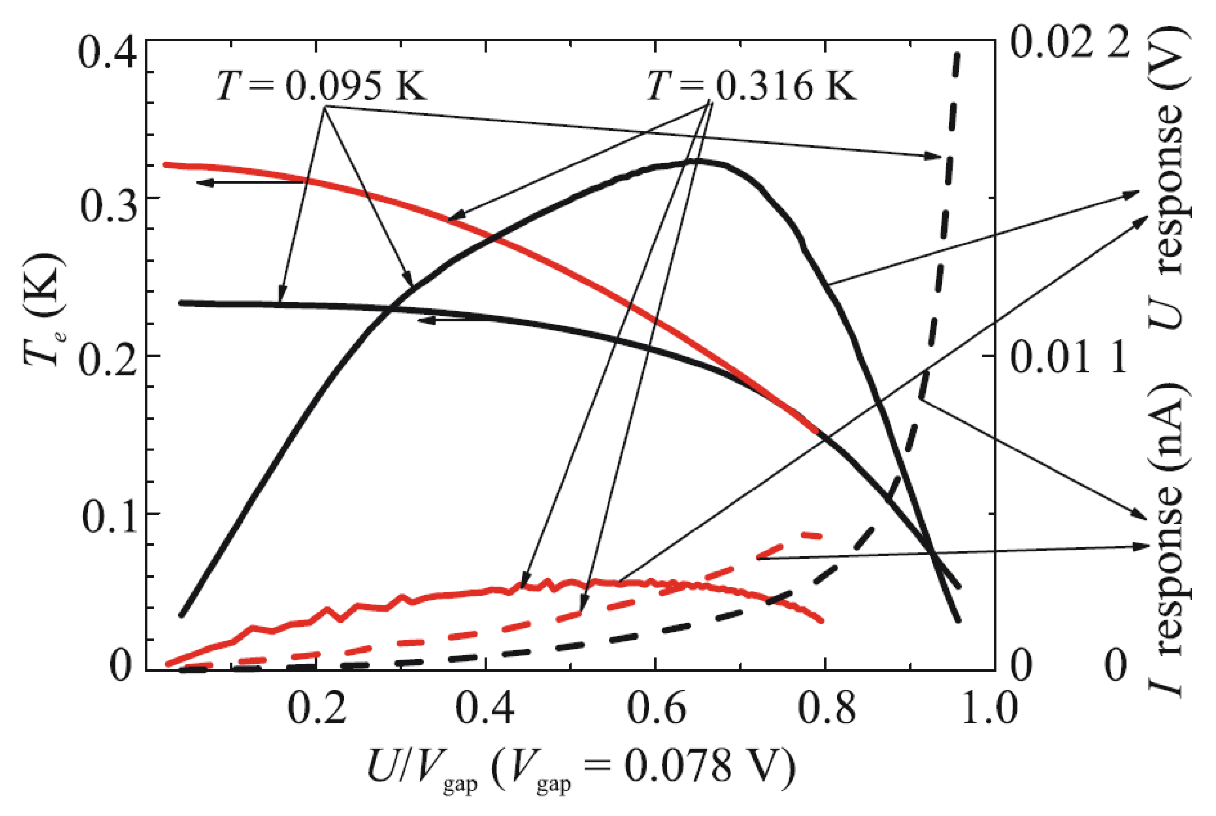
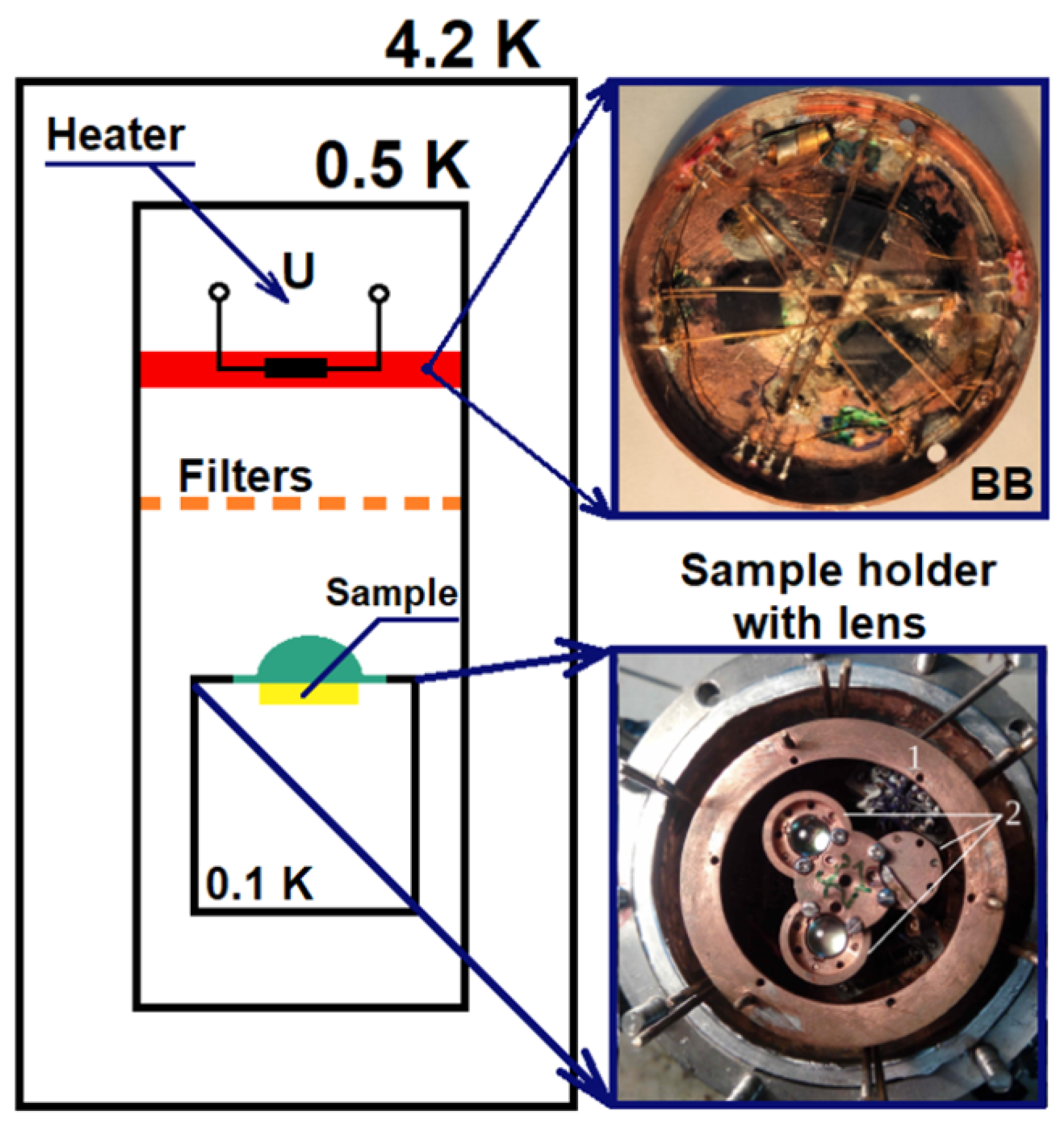
6. Experimental Studies
7. Applications of SINIS Detectors
8. Discussion
9. Conclusions
10. Patents
- Tarasov, M.; Nagirnaya, D.; Gunbina, A.; Fominsky, M.; Yusupov, R. Metal-Dielectric-Metal-Dielectric-Metal photodetector, Patent RU2749575C1, Russia, date of publication: 15 June 2021, priority: 7 September 2020.
- Tarasov, M.; Gunbina, A.; Nagirnaya, D.; Fominskii, M. Method of Making Device with Thin-Film Tunnel Junctions, Patent RU2733330C1, date of publication: 1 October 2020, priority: 22 July 2019.
- Tarasov, M.; Gunbina, A.; Fominsky, M.; Chekushkin, A.; Method of fabrication of thin-film tunnel junctions by means of separate lithography, application for patent, Patent RU2757762C1, date of publication: 21 October 2021, priority: 30 March 2021.
- Tarasov, M.; Chekushkin, A.; Yusupov, R. Method of fabrication devices with free-standing microbridges, Patent RU2632630C1, date of publication: 6 October 2017, priority: 6 June 2016.
Author Contributions
Funding
Institutional Review Board Statement
Informed Consent Statement
Acknowledgments
Conflicts of Interest
References
- Giazotto, F.; Heikkilä, T.T.; Luukanen, A. Electronic Refrigeration: Physics and Applications. Available online: https://arxiv.org/pdf/cond-mat/0508093v1.pdf (accessed on 19 September 2022).
- Ullom, J.N. Physics and applications of NIS junctions. Proc. AIP Conf. 2002, 605, 135–140. [Google Scholar] [CrossRef] [Green Version]
- Tarasov, M.; Edelman, V. Nanodevices with Normal Metal—Insulator—Superconductor Tunnel Junctions. In Functional Nanostructures and Metamaterials for Superconducting Spintronics: From Superconducting Qubits to Self-Organized Nanostructures; Sidorenko, A., Ed.; Springer International Publishing AG: Cham, Switzerland, 2018; pp. 91–116. [Google Scholar] [CrossRef]
- Vystavkin, A.; Shuvaev, D.; Kuz’min, L.; Tarasov, M.A.; Aderstedt, E.; Claeson, M.W.T. Normal-metal hot-electron bolometer with Andreev reflection from superconductor boundaries. J. Exp. Theor. Phys. 1999, 88, 598–602. [Google Scholar] [CrossRef]
- Nahum, M.; Richards, P.; Mears, C. Design analysis of a novel hot-electron microbolometer. IEEE Trans. Appl. Supercond. 1993, 3, 2124–2127. [Google Scholar] [CrossRef]
- Chouvaev, D.; Sandgren, D.; Tarasov, M.; Kuzmin, L. Optical Qualification of the Normal Metal Hot-Electron Microbolometer (NHEB). In Proceedings of the 12th International Symposium on Space Terahertz Technology, San Diego, CA, USA, 14–16 February 2001. [Google Scholar]
- Kuzmin, L.S. Cold-Electron bolometers. In Bolometers; Perera, A.G.U., Ed.; InTech: Rijeka, Croatia, 2012; p. 77. ISBN 978-953-51-0235-9. [Google Scholar]
- Brien, T.L.R.; Ade, P.A.R.; Barry, P.S.; Dunscombe, C.; Leadley, D.R.; Morozov, D.V.; Myronov, M.; Parker, E.H.; Prest, M.J.; Prunnila, M.; et al. A strained silicon cold electron bolometer using Schottky contacts. Appl. Phys. Lett. 2014, 105, 043509. [Google Scholar] [CrossRef] [Green Version]
- Schmidt, D.R.; Duncan, W.D.; Irwin, K.D.; Lehnert, K.W.; Miller, N.A.; Ullom, J.N. Normal metal–insulator–superconductor junction technology for bolometers. Nucl. Instrum. Methods Phys. Res. Sect. A Accel. Spectrom. Detect. Assoc. Equip. 2006, 559, 516–518. [Google Scholar] [CrossRef]
- Schmidt, D.R.; Lehnert, K.W.; Clark, A.M.; Duncan, W.D.; Irwin, K.D.; Miller, N.; Ullom, J.N. A superconductor–insulator–normal metal bolometer with microwave readout suitable for large-format arrays. Appl. Phys. Lett. 2005, 86, 053505. [Google Scholar] [CrossRef]
- Tarasov, M.; Gunbina, A.; Mansfeld, M.; Yakopov, G.; Chekushkin, A.; Yusupov, R.; Lemzyakov, S.; Edelman, V.; Vdovin, V. Arrays of annular cryogenic antennas with SINIS bolometers and cryogenic receivers for SubTHz observatories. EPJ Web Conf. 2018, 195, 05010. [Google Scholar] [CrossRef]
- Devyatov, I.A.; Krutitskii, P.A.; Kupriyanov, M.Y. Investigation of various operation modes of a miniature superconducting detector of microwave radiation. JETP Lett. 2006, 84, 57–61. [Google Scholar] [CrossRef]
- Devyatov, I.A.; Kupriyanov, M.Y. Investigation of a nonequilibrium electron subsystem in low-temperature microwave detectors. JETP Lett. 2004, 80, 646–650. [Google Scholar] [CrossRef]
- Yusupov, R.A.; Gunbina, A.A.; Chekushkin, A.M.; Nagirnaya, D.V.; Lemzyakov, S.A.; Edel’man, V.S.; Tarasov, M.A. Quantum response of a bolometer based on the SINIS structure with a suspended absorber. Phys. Solid State 2020, 62, 1567–1570. [Google Scholar] [CrossRef]
- Feshchenko, A.V.; Casparis, L.; Khaymovich, I.M.; Maradan, D.; Saira, O.P.; Palma, M.; Meschke, M.; Pekola, J.P.; Zumbühl, D.M. Tunnel-Junction Thermometry Down to Millikelvin Temperatures. Phys. Rev. Appl. 2015, 4, 034001. [Google Scholar] [CrossRef] [Green Version]
- Pekola, J. Trends in Thermometry. J. Low Temp. Phys. 2004, 135, 723–744. [Google Scholar] [CrossRef]
- Isosaari, E.; Holmqvist, T.; Meschke, M.; Heinonen, M.; Pekola, J.P. Thermometry by micro and nanodevices. Eur. Phys. J. Spec. Top. 2009, 172, 323–332. [Google Scholar] [CrossRef]
- Pekola, J.P.; Manninen, A.J.; Leivo, M.M.; Arutyunov, K.; Suoknuuti, J.K.; Suppula, T.I.; Collaudin, B. Microrefrigeration by quasiparticle tunneling in NIS and SIS junctions. Phys. B Condens. Matter 2000, 280, 485–490. [Google Scholar] [CrossRef]
- Nguyen, H.Q.; Aref, T.; Kauppila, V.J.; Meschke, M.; Winkelmann, C.B.; Courtois, H.; Pekola, J.P. Trapping hot quasi-particles in a high-power superconducting electronic cooler. New J. Phys. 2013, 5, 085013. [Google Scholar] [CrossRef]
- Clark, A.M.; Miller, N.A. Cooling of bulk material by electron-tunneling refrigerators. Appl. Phys. Lett. 2005, 86, 173508. [Google Scholar] [CrossRef]
- O’Neil, G.C. Improving NIS Tunnel Junction Refrigerators: Modeling, Materials, and Traps. Ph.D. Thesis, University of Colorado, Boulder, CO, USA, 2011. [Google Scholar]
- Kuzmin, L.; Fominsky, M.; Kalabukhov, A.; Golubev, D.; Tarasov, M. Capacitively Coupled Hot-Electron Nanobolometer with SIN Tunnel Junctions. In Proceedings of the SPIE Volume 4855: Millimeter and Submillimeter Detectors for Astronomy, Astronomical Telescopes and Instrumentation, Waikoloa, HI, USA, 17 February 2003. [Google Scholar] [CrossRef]
- Tarasov, M.; Nagirnaya, D.; Gunbina, A.; Fominsky, M.; Yusupov, R. Metal-Dielectric-Metal-Dielectric-Metal Photodetector. Patent RU2749575C1, 15 June 2021. [Google Scholar]
- Tarasov, M.; Edelman, V.; Lemzyakov, S.; Gunbina, A.A.; Yusupov, R.A.; Chekushkin, A.M.; Nagirnaya, D.V.; Vdovin, V.F.; Kalaboukhov, A. Cryogenic Mimim and Simis Microwave Detectors. In Proceedings of the 7th All-Russian Microwave Conference (RMC), Moscow, Russia, 25–27 November 2020; pp. 25–27. [Google Scholar] [CrossRef]
- Tarasov, M.; Fominsky, M.; Kalabukhov, A.; Kuzmin, L. Experimental study of a bolometer on hot electrons in normal metal with capacitive coupling. JETP Lett. 2002, 76, 507–510. [Google Scholar] [CrossRef]
- Nahum, M.; Eiles, T.M.; Martinis, J.M. Electronic microrefrigerator based on a normal-insulator-superconductor tunnel junction. Appl. Phys. Lett. 1994, 65, 3123–3125. [Google Scholar] [CrossRef]
- Leivo, M.M.; Pekola, J.P.; Averin, D.V. Efficient Peltier refrigeration by a pair of normal metal/insulator/superconductor junctions. Appl. Phys. Lett. 1996, 68, 1996–1998. [Google Scholar] [CrossRef] [Green Version]
- Kuzmin, L.S.; Devyatov, I.A.; Golubev, D. Cold-electron bolometer with electronic microrefrigeration and general noise analysis. In Proceedings of the Millimeter and Submillimeter Waves IV Volume 3465, SPIE’s International Symposium on Optical Science, Engineering, and Instrumentation, San Diego, CA, USA, 13 November 1998; pp. 193–199. [Google Scholar]
- Golubev, D.; Kuzmin, L. Nonequilibrium theory of a hot-electron bolometer with normal metal-insulator-superconductor tunnel junction. J. Appl. Phys. 2001, 89, 6464. [Google Scholar] [CrossRef]
- Gunbina, A.; Lemzyakov, S.; Tarasov, M.; Edelman, V.S.; Yusupov, R.A.B. Response of a SINIS detector with electron cooling to submillimeter-wave radiation. JETP Lett. 2020, 11, 539–542. [Google Scholar] [CrossRef]
- Tarasov, M.; Gunbina, A.; Yusupov, R.; Chekushkin, A.; Nagirnaya, D.; Lemzyakov, S.; Vdovin, V.; Edelman, V.; Kalaboukhov, A.; Winkler, D. Thermal absorption and quantum efficiency of SINIS bolometer. IEEE Trans. Appl. Supercond. 2021, 31, 2300105. [Google Scholar] [CrossRef]
- Chekushkin, A.; Tarasov, M.; Yusupov, R.; Edelman, V. Influence of normal metal traps, Andreev reflection and proximity effect on superconductor cooling in SINIS-structures. Work. MIPT 2018, 10, 64–71. [Google Scholar]
- Gunbina, A.; Tarasov, M.; Fominsky, M.; Chekushkin, A.; Yusupov, R.; Nagirnaya, D. Fabrication of Aluminium Nanostructures for Microwave Detectors Based on Tunnel Junctions. In Advances in Microelectronics Reviews; Yurish, S.Y., Ed.; IFSA Publishing, S.L.: Barcelona, Spain, 2021; Volume 3, pp. 183–212. [Google Scholar]
- Dolan, G.J. Offset mask for lift-off photoprocessing. Appl. Phys. Lett. 1977, 31, 337–339. [Google Scholar] [CrossRef]
- Lecocq, F.; Pop, I.M.; Peng, Z.; Matei, I.; Crozes, T.; Fournier, T.; Naud, C.; Guichard, W.; Buisson, O. Junction fabrication by shadow evaporation without a suspended bridge. Nanotechnology 2011, 22, 315302. [Google Scholar] [CrossRef] [PubMed] [Green Version]
- Tarasov, M.; Gunbina, A.; Nagirnaya, D.; Fominsky, M. Method of Making Device with Thin-Film Tunnel Junctions. Patent RU2733330C1, 1 October 2020. [Google Scholar]
- Otto, E.; Tarasov, M.; Grimes, P.; Chekushkin, A.; Kuzmin, L.S.; Yassin, G. Optical response of a titanium-based cold-electron bolometer. Supercond. Sci. Technol. 2013, 26, 085020. [Google Scholar] [CrossRef] [Green Version]
- Tarasov, M.; Gunbina, A.; Fominsky, M.; Chekushkin, A. Method of Fabrication of Thin-Film Tunnel Junctions by Means of Separate Lithography, Application for Patent. Patent RU2757762C1, 21 October 2021. [Google Scholar]
- Tarasov, M.; Edelman, V.; Mahashabde, S.; Fominsky, M.; Lemzyakov, S.; Chekushkin, A.; Yusupov, R.; Winkler, D.; Yurgens, A. Electrical and optical properties of a bolometer with a suspended absorber and tunneling-current thermometers. Appl. Phys. Lett. 2017, 110, 242601. [Google Scholar] [CrossRef] [Green Version]
- Tarasov, M.; Edelman, V.; Mahashabde, S.; Fominsky, M.; Lemzyakov, S.; Chekushkin, A.; Yusupov, R.; Winkler, D.; Yurgens, A. SINIS bolometer with a suspended absorber. J. Phys. Conf. Ser. 2017, 969, 012088. [Google Scholar] [CrossRef]
- Tarasov, M.; Chekushkin, A.; Yusupov, R. Method of Fabrication Devices with Free-Standing Microbridges. Patent RU2632630C1, 6 October 2017. [Google Scholar]
- Edelman, V.S. A dilution microcryostat-insert. Instrum. Exp. Tech. 2009, 52, 301–307. [Google Scholar] [CrossRef]
- Lemzyakov, S. Interaction of SINIS Structures with Submillimeter-Wave Radiation. Ph.D. Thesis, P. Kapitza Institute for Physical Problems, Moscow, Russia, 2020. [Google Scholar]
- Pfeiffer, U. Integrated Circuit Design for Terahertz Applications. 6G Wireless Summit. 2019; 201p. [Google Scholar]
- Lu, X.; Venkatesh, S.; Saeidi, H. A Review on Applications of Integrated Terahertz Systems. China Commun. 2021, 18, 175–201. [Google Scholar] [CrossRef]
- Pavlidis, D. Fundamentals of Terahertz Devices and Applications; John Wiley & Sons: Hoboken, NJ, USA, 2021; 576p, ISBN 1119460735. [Google Scholar]
- Beckman, J.E. Radioastronomy. In Multimessenger Astronomy; Springer International Publishing AG: Cham, Switzerland, 2021; pp. 45–79. [Google Scholar] [CrossRef]
- Hojaev, A.S.; Zinchenko, I.I. Scientific Problems and Possibilities of Studying Extended Molecular Clouds with RT-70. Bull. Lebedev Phys. Inst. 2021, 48, 272–280. [Google Scholar] [CrossRef]
- Editors: Ghzaoui, M.E.; Das, S.; Lenka, T.R.; Biswas, A. Terahertz Wireless Communication Components and System Technologies; Springer International Publishing AG: Cham, Switzerland, 2022; ISBN 978-981-16-9181-2. [Google Scholar]
- Chaccour, C.; Soorki, M.N.; Saad, W.; Bennis, M.; Popovski, P.; Debbah, M. Seven Defining Features of Terahertz (THz) Wireless Systems: A Fellowship of Communication and Sensing. IEEE Commun. Surv. Tutor. 2022, 24, 967–993. [Google Scholar] [CrossRef]
- Akyildiz, I.F.; Han, C.; Hu, Z.; Nie, S.; Jornet, J.M. Terahertz Band Communication: An Old Problem Revisited and Research Directions for the Next Decade. IEEE Trans. Commun. 2022, 70, 4250–4285. [Google Scholar] [CrossRef]
- Meenakshi; Saurav, P.; Kishor, K. Design and simulation of metamaterial under the THz frequency for short-range wireless communication and military purposes. Mater. Today Proc. 2022, 62, 3729–3733. [Google Scholar] [CrossRef]
- Ergün, S.; Sönmez, S. Terahertz Technology for Military Applications. J. Manag. Inf. Sci. 2015, 3, 13–16. [Google Scholar] [CrossRef]
- Dodson, C.; Fitch, M.J.; Osiander, R.; Spicer, J.B. Terahertz imaging for anti-personnel mine detection. Proc. Terahertz Mil. Sec. Appl. III 2005, 5790, 85–93. [Google Scholar] [CrossRef]
- Rappaport, T.S.; Xing, Y.; Kanhere, O.; Ju, S. Wireless Communications and Applications Above 100 GHz: Opportunities and Challenges for 6G and Beyond. IEEE Access. 2019, 7, 78729–78757. [Google Scholar] [CrossRef]
- Kuzmin, L.S.; Pankratov, A.L.; Gordeeva, A.V.; Zbrozhek, V.O.; Shamporov, V.A.; Revin, L.S.; Blagodatkin, A.V.; Masi, S.; de Bernardis, P. Photon-noise-limited cold-electron bolometer based on strong electron self-cooling for high-performance cosmology missions. Commun. Phys. 2019, 2, 104. [Google Scholar] [CrossRef] [Green Version]
- Tarasov, M.; Kuzmin, L.; Stepantsov, E.; Agulo, I.; Kalabukhov, A.; Fominskii, M.; Ivanov, Z.; Claeson, T. Terahertz spectroscopy by Josephson oscillator and SINIS bolometer. JETP Lett. 2004, 79, 298–303. [Google Scholar] [CrossRef]


| Operation Mode | Current Responsivity | dI/dP (A/W) | dV/dP (V/W) |
|---|---|---|---|
| Photon counter with electron cooling | e/hf | 762 | 2.6 × 10⁷ |
| Practical detector at half gap where Rd = 35 kΩ | 2/VΔ | 5 × 10³ | 1.75 × 10⁸ |
| Quantum detector close to gap where Rd = 2 kΩ | e/2kT | 2.2 × 10⁴ | 4.4 × 10⁷ |
| Electric detector at dc | 2k/(RdeΣνT4) | 3.7 × 10⁵ | 1.3 × 10¹⁰ |
| Shadow Technique | ||
|---|---|---|
| Dolan’s Bridges | Bridge-Free Technology | |
| Short description |
|
|
| Schematic image of process | 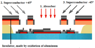 | 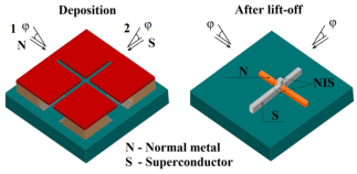 |
| Advantages | Deposition in one vacuum cycle, one lithography | Deposition in one technological process—this technology overcomes the disadvantages of Dolan’s suspended bridges |
| Disadvantages | Possibility of breaking the suspended resist bridge, not completely removing vertical walls, possibly bending the upper layer of the resist; only e-beam lithography; specialized deposition equipment | The common drawback for both shadow evaporation methods is that they require directional evaporation and are not applicable for magnetron sputtering; only e-beam lithography; specialized deposition equipment |
| Direct-Write Technology | ||
|---|---|---|
| Direct-Write Trilayer Technology | Direct-Write Technology | |
| Short description |
|
|
| Schematic image of process | 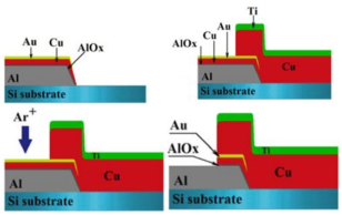 | 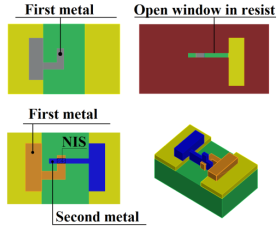 |
| Advantages | Any type of lithography | Can be applicable for industrial processes of magnetron sputtering and plasma etching. Such process bring flexibility in the choice of metal film materials and the possibility of creating a high-quality tunnel barrier. Any type of lithography |
| Disadvantages | Three technological cycles, additional layers for passivation | Two technological cycles |
Publisher’s Note: MDPI stays neutral with regard to jurisdictional claims in published maps and institutional affiliations. |
© 2022 by the authors. Licensee MDPI, Basel, Switzerland. This article is an open access article distributed under the terms and conditions of the Creative Commons Attribution (CC BY) license (https://creativecommons.org/licenses/by/4.0/).
Share and Cite
Tarasov, M.; Gunbina, A.; Chekushkin, A.; Yusupov, R.; Edelman, V.; Koshelets, V. Microwave SINIS Detectors. Appl. Sci. 2022, 12, 10525. https://doi.org/10.3390/app122010525
Tarasov M, Gunbina A, Chekushkin A, Yusupov R, Edelman V, Koshelets V. Microwave SINIS Detectors. Applied Sciences. 2022; 12(20):10525. https://doi.org/10.3390/app122010525
Chicago/Turabian StyleTarasov, Mikhail, Aleksandra Gunbina, Artem Chekushkin, Renat Yusupov, Valerian Edelman, and Valery Koshelets. 2022. "Microwave SINIS Detectors" Applied Sciences 12, no. 20: 10525. https://doi.org/10.3390/app122010525