

T-Type Vertical Wall for Decoupling and Pattern Correction of Patch Antenna
 and
and 
Abstract
:1. Introduction
2. Antenna Configuration and Parametric Analysis
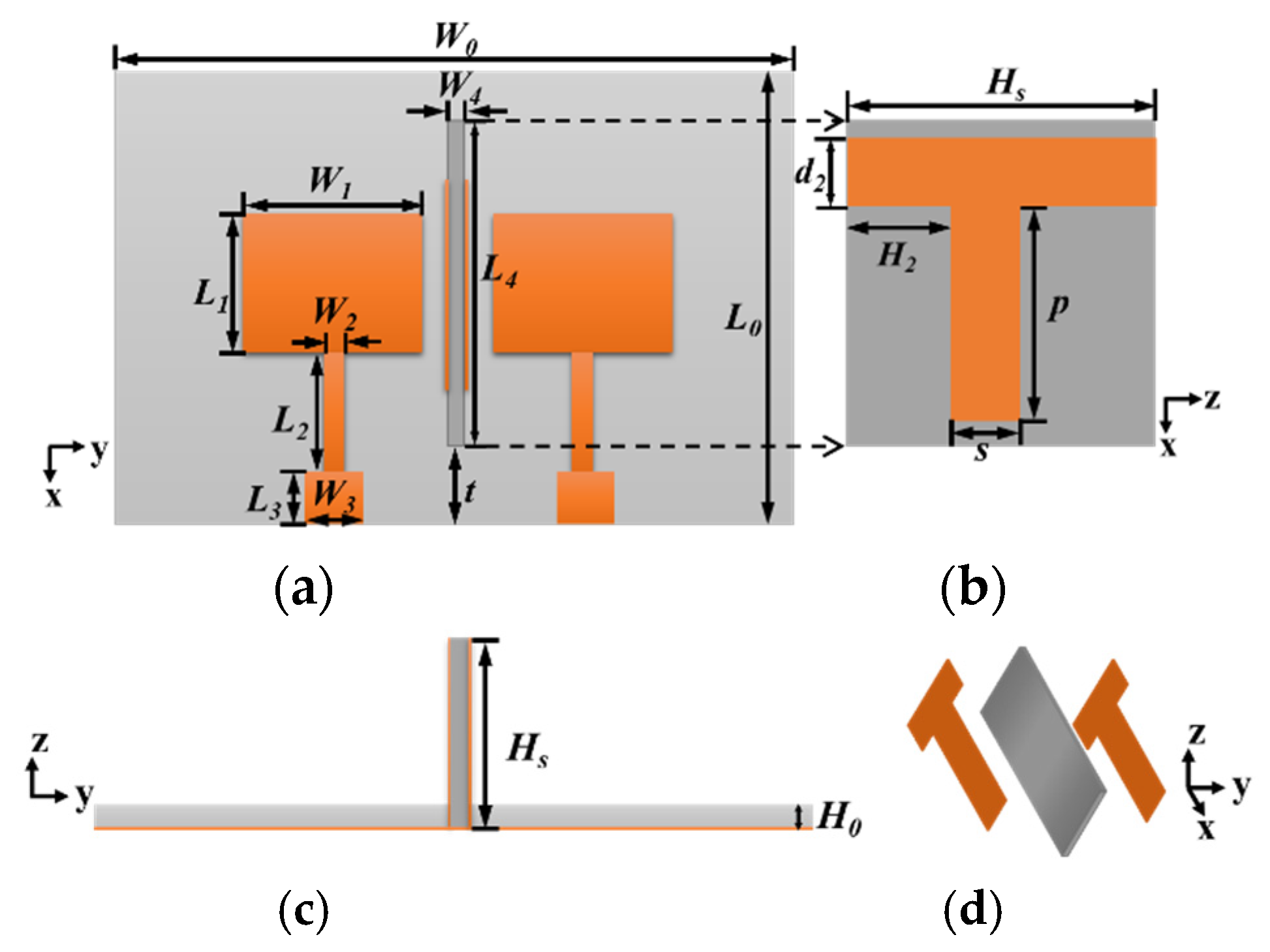
2.1. Configuration
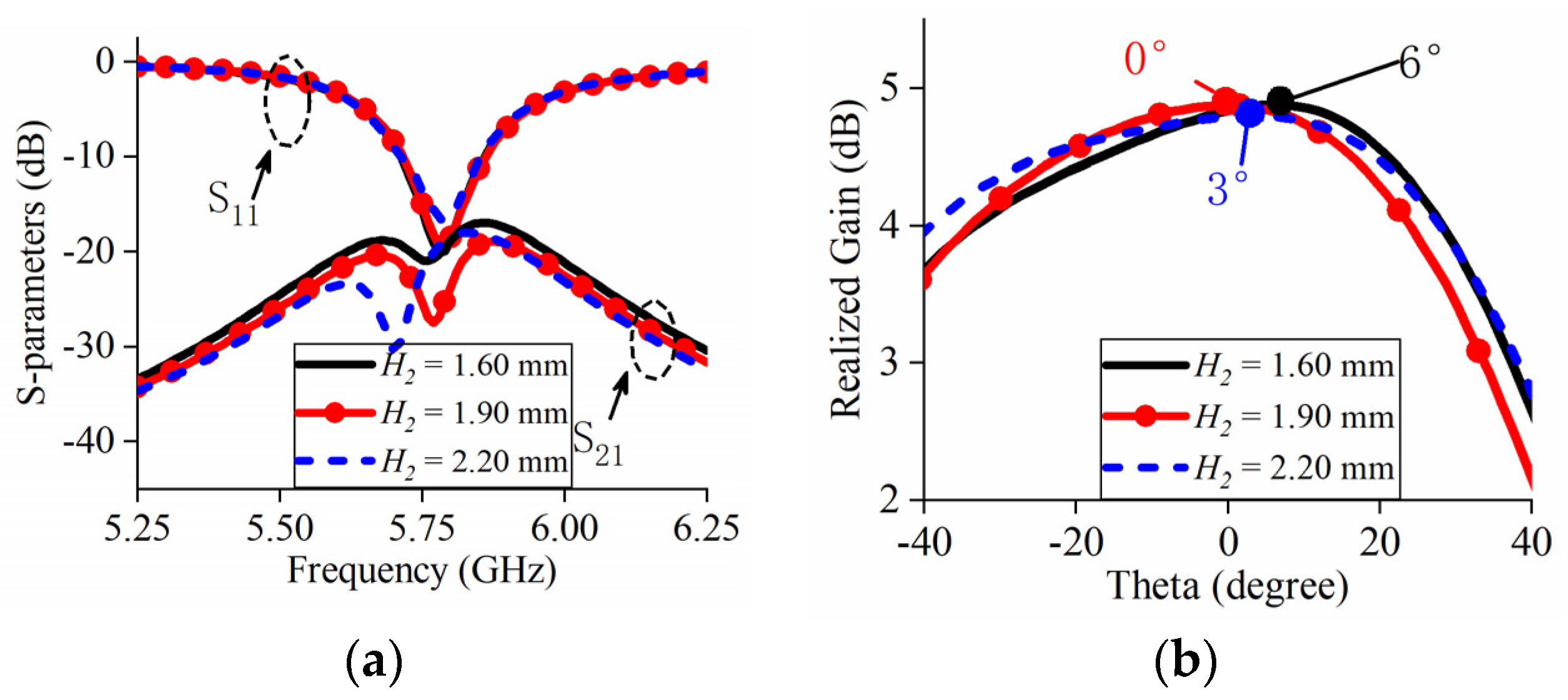
2.2. Parametric Analyses
3. Result Analyses
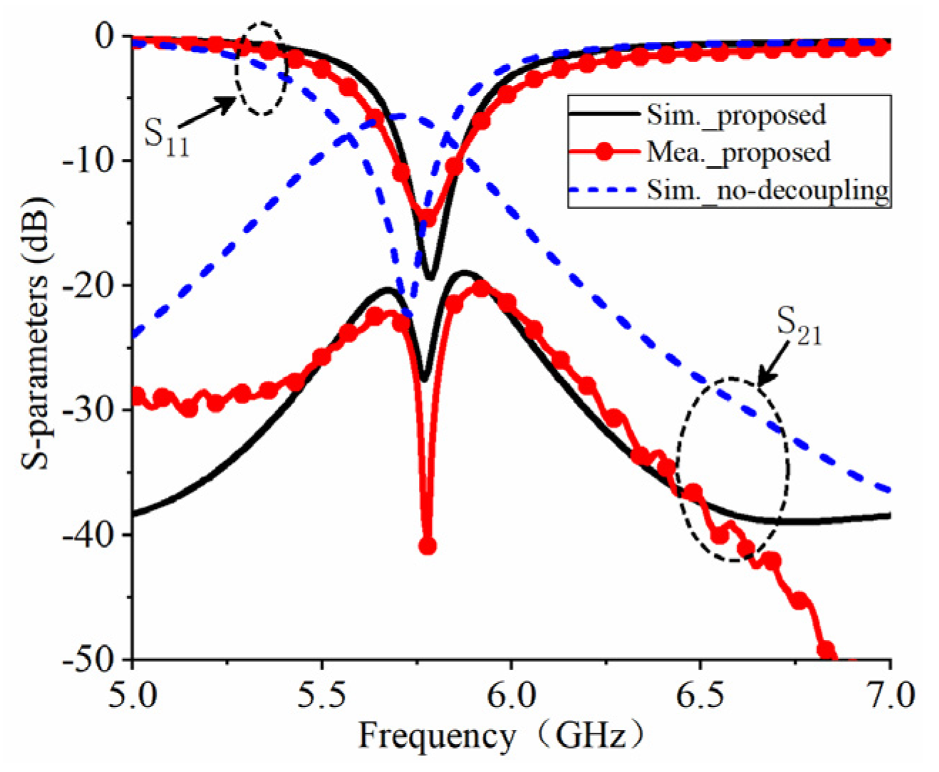
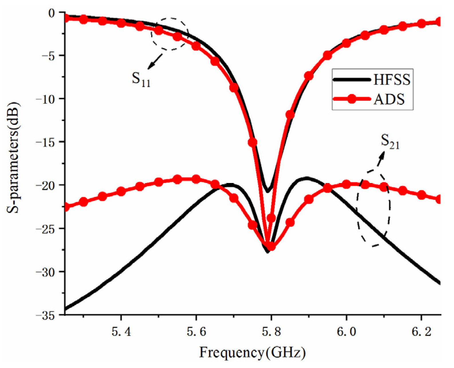
3.1. S-Parameters
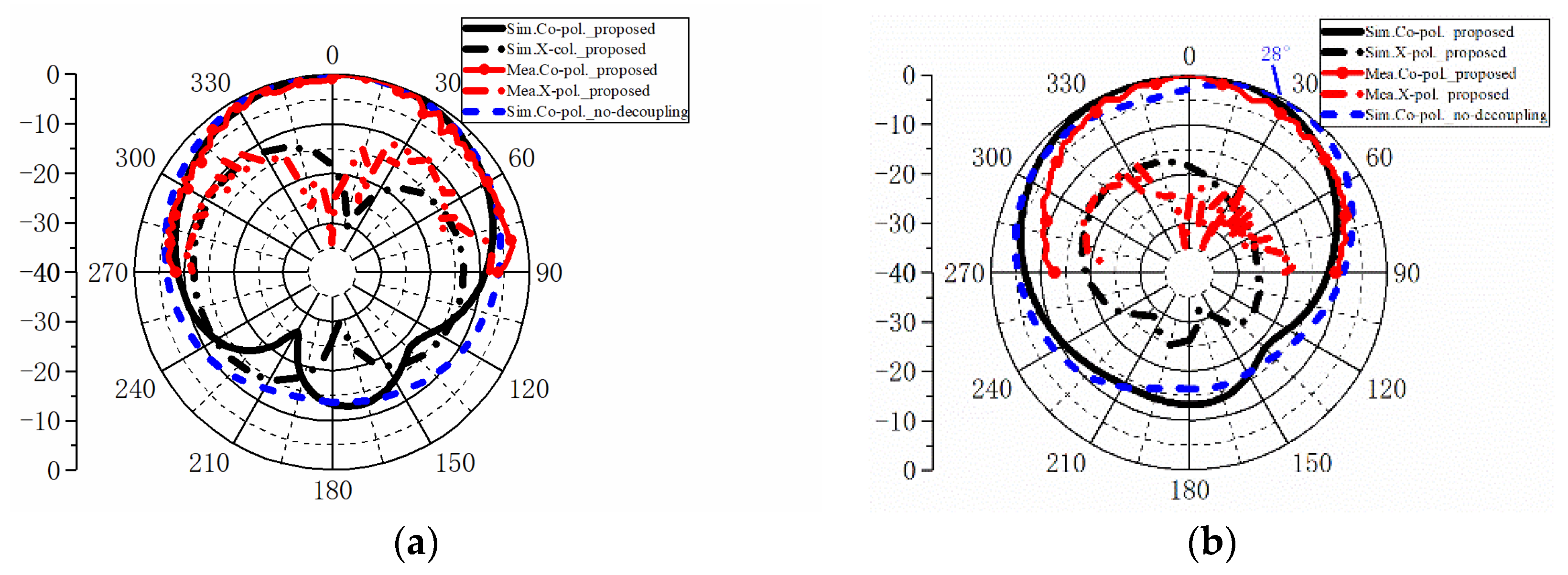
3.2. Pattern and Realized Gain
3.3. Comparison with Other Works
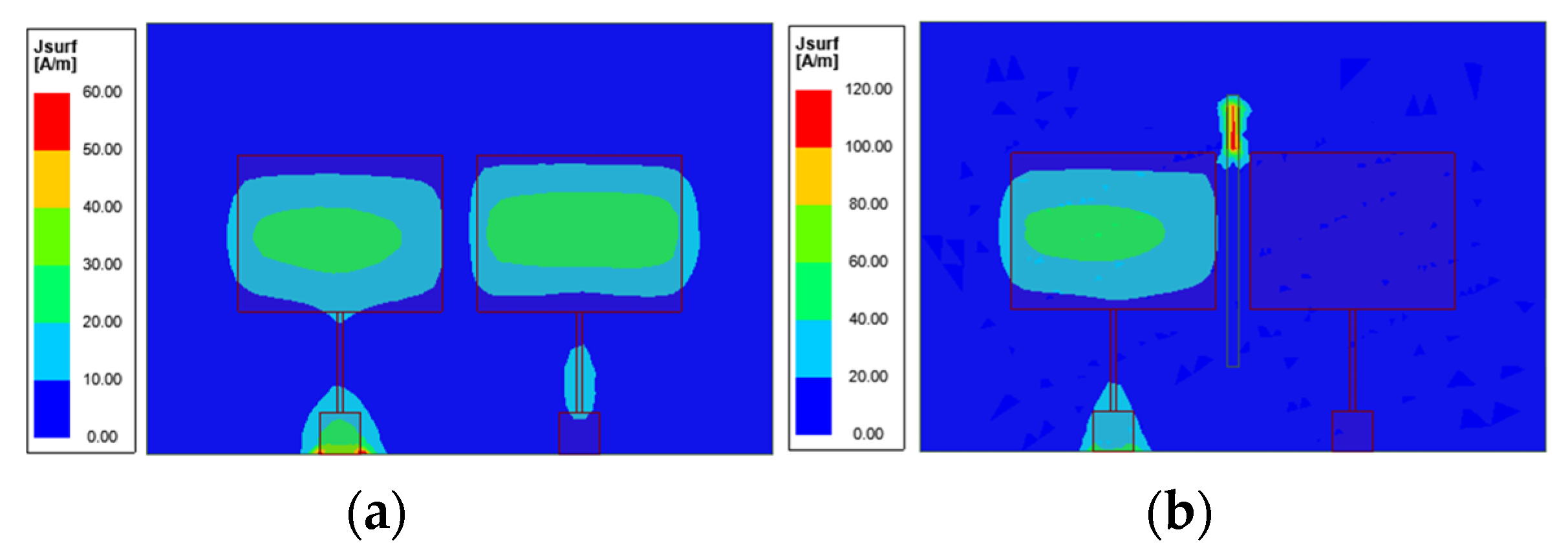
3.4. Current Distribution Comparison
4. Mechanism and Equivalent Circuit Analyses
5. Conclusions
Author Contributions
Funding
Institutional Review Board Statement
Informed Consent Statement
Data Availability Statement
Conflicts of Interest
References
- Li, M.; Zhong, B.G.; Cheung, S.W. Isolation Enhancement for MIMO Patch Antennas Using Near-Field Resonators as Coupling-Mode Transducers. IEEE Trans. Antennas Propag. 2019, 67, 755–764. [Google Scholar] [CrossRef]
- Niu, Z.; Zhang, H.; Chen, Q.; Zhong, T. Isolation Enhancement in Closely Coupled Dual-Band MIMO Patch Antennas. IEEE Antennas Wirel. Propag. Lett. 2019, 18, 1686–1690. [Google Scholar] [CrossRef]
- Li, M.; Jamal, M.Y.; Jiang, L.; Yeung, K.L. Isolation Enhancement for MIMO Patch Antennas Sharing a Common Thick Substrate: Using a Dielectric Block to Control Space-Wave Coupling to Cancel Surface-Wave Coupling. IEEE Trans. Antennas Propag. 2021, 69, 1853–1863. [Google Scholar] [CrossRef]
- Qamar, Z.; Naeem, U.; Khan, S.A.; Chongcheawchamnan, M.; Shafique, M.F. Mutual Coupling Reduction for High-Performance Densely Packed Patch Antenna Arrays on Finite Substrate. IEEE Trans. Antennas Propag. 2016, 64, 1653–1660. [Google Scholar] [CrossRef]
- Mohamadzade, B.; Afsahi, M. Mutual coupling reduction and gain enhancement in patch array antenna using a planar compact electromagnetic bandgap structure. IET Microw. Antennas Propag. 2017, 11, 1719–1725. [Google Scholar] [CrossRef]
- Yang, X.M.; Liu, X.G.; Zhou, X.Y.; Cui, T.J. Reduction of Mutual Coupling between Closely Packed Patch Antennas Using Waveguided Metamaterials. IEEE Antennas Wirel. Propag. Lett. 2012, 11, 389–391. [Google Scholar] [CrossRef]
- Alsath, M.G.N.; Kanagasabai, M.; Balasubramanian, B. Implementation of Slotted Meander-Line Resonators for Isolation Enhancement in Microstrip Patch Antenna Arrays. IEEE Antennas Wirel. Propag. Lett. 2013, 12, 15–18. [Google Scholar] [CrossRef]
- Yang, X.; Liu, Y.; Xu, Y.-X.; Gong, S.-X. Isolation Enhancement in Patch Antenna Array with Fractal UC-EBG Structure and Cross Slot. IEEE Antennas Wirel. Propag. Lett. 2017, 16, 2175–2178. [Google Scholar] [CrossRef]
- Vishvaksenan, K.S.; Mithra, K.; Kalaiarasan, R.; Raj, K.S. Mutual Coupling Reduction in Microstrip Patch Antenna Arrays Using Parallel Coupled-Line Resonators. IEEE Antennas Wirel. Propag. Lett. 2017, 16, 2146–2149. [Google Scholar] [CrossRef]
- Qi, H.; Yin, X.; Liu, L.; Rong, Y.; Qian, H. Improving Isolation between Closely Spaced Patch Antennas Using Interdigital Lines. IEEE Antennas Wirel. Propag. Lett. 2016, 15, 286–289. [Google Scholar] [CrossRef]
- Hwangbo, S.; Yang, H.Y.; Yoon, Y.-K. Mutual Coupling Reduction Using Micromachined Complementary Meander-Line Slots for a Patch Array Antenna. IEEE Antennas Wirel. Propag. Lett. 2017, 16, 1667–1670. [Google Scholar] [CrossRef]
- Wei, K.; Li, J.-Y.; Wang, L.; Xing, Z.-J.; Xu, R. Mutual Coupling Reduction by Novel Fractal Defected Ground Structure Bandgap Filter. IEEE Trans. Antennas Propag. 2016, 64, 4328–4335. [Google Scholar] [CrossRef]
- OuYang, J.; Yang, F.; Wang, Z.M. Reducing Mutual Coupling of Closely Spaced Microstrip MIMO Antennas for WLAN Application. IEEE Antennas Wirel. Propag. Lett. 2011, 10, 310–313. [Google Scholar] [CrossRef]
- Niu, Z.-C.; Zhang, H.; Chen, Q.; Zhang, T. Isolation Enhancement for 1 × 3 Closely Spaced E-Plane Patch Antenna Array Using Defect Ground Structure and Metal-Vias. IEEE Access 2019, 7, 119375–119383. [Google Scholar] [CrossRef]
- Ghannad, A.A.; Khalily, M.; Xiao, P.; Tafazolli, R.; Kishk, A.A. Enhanced Matching and Vialess Decoupling of Nearby Patch Antennas for MIMO System. IEEE Antennas Wirel. Propag. Lett. 2019, 18, 1066–1070. [Google Scholar] [CrossRef]
- Qi, H.; Liu, L.; Yin, X.; Zhao, H.; Kulesza, W.J. Mutual Coupling Suppression between Two Closely Spaced Microstrip Antennas with an Asymmetrical Coplanar Strip Wall. IEEE Antennas Wirel. Propag. Lett. 2016, 15, 191–194. [Google Scholar] [CrossRef]
- Li, M.; Tian, S.; Tang, M.-C.; Zhu, L. A Compact Low-Profile Hybrid-Mode Patch Antenna with Intrinsically Combined Self-Decoupling and Filtering Properties. IEEE Trans. Antennas Propag. 2022, 70, 1511–1516. [Google Scholar] [CrossRef]
- Pei, T.; Zhu, L.; Wang, J.; Wu, W. A Low-Profile Decoupling Structure for Mutual Coupling Suppression in MIMO Patch Antenna. IEEE Trans. Antennas Propag. 2021, 69, 6145–6153. [Google Scholar] [CrossRef]
- Fang, Y.; Tang, M.; Zhang, Y.P. A Decoupling Structure for Mutual Coupling Suppression in Stacked Microstrip Patch Antenna Array. IEEE Antennas Wirel. Propag. Lett. 2022, 21, 1110–1114. [Google Scholar] [CrossRef]
- Sun, X.-B.; Cao, M.-Y. Low mutual coupling antenna array for WLAN application. Electron. Lett. 2017, 53, 368–370. [Google Scholar] [CrossRef]
- Lin, H.; Chen, Q.; Ji, Y.; Yang, X.; Wang, J.; Ge, L. Weak-Field-Based Self-Decoupling Patch Antennas. IEEE Trans. Antennas Propag. 2020, 68, 4208–4217. [Google Scholar] [CrossRef]
- Lai, Q.-X.; Pan, Y.-M.; Zheng, S.-Y.; Yang, W.-J. Mutual Coupling Reduction in MIMO Microstrip Patch Array Using TM10 and TM02 Modes. IEEE Trans. Antennas Propag. 2021, 69, 7562–7571. [Google Scholar] [CrossRef]
- Wang, Y.-Y.; Zhang, S.-F.; Yan, Y.-T.; Yu, X.-H.; Kishk, A.A. Vertical-Wall between Tightly Spaced Patch Antennas for Decoupling and Radiation Pattern Correction. In Proceedings of the IEEE International Symposium on Antennas and Propagation and USNC-URSI Radia Science Meeting (APS/URSI), Singapore, 4–10 December 2021. [Google Scholar]


| Variable | Value (mm) | Variable | Value (mm) | Variable | Value (mm) |
|---|---|---|---|---|---|
| W0 | 46 | L2 | 7.5 | p | 14 |
| L0 | 31.7 | W3 | 3 | t | 6.25 |
| HS | 6.4 | L3 | 3 | s | 1.98 |
| W1 | 15 | W4 | 0.8 | d2 | 3.1 |
| L1 | 11.5 | L4 | 20 | H0 | 1.6 |
| W2 | 0.5 | H2 | 1.9 |
| Literature | Placement Orientation | Decoupling Technique | Center Frequency | Edge-to-Edge Spacing | Tilt |
|---|---|---|---|---|---|
| [3] | E-plane | Dielectric Block | 10.00 GHz | 0.027 | ~10° |
| [10] | H-plane | Three Interdigital Lines | 5.80 GHz | 0.07 | ~30° |
| [11] | E-plane | Meander-line Slots | 5.00 GHz | 0.06 | ~30° |
| [13] | E-plane | Ground Slot | 5.80 GHz | 0.031 | ~45° |
| [14] | E-plane | Slotted Ground | 4.00 GHz | 0.037 | ~30° |
| [15] | H-plane | Metal Stub & Slotted Ground | 5.50 GHz | 0.018 | ~25° |
| [16] | H-plane | Asymmetrical Coplanar Strip Wall | 5.80 GHz | 0.03 | ~30° |
| [18] | H-plane | Half-wave Microstrip Line & Shorting Pin | 3.16 GHz | 0.027 | ~30° |
| Our Work | H-plane | T-type Metal Wall | 5.80 GHz | 0.05 | 0° |
| Component | R1 | L1 | C1 | R2 | L2 | C2 | C3 |
|---|---|---|---|---|---|---|---|
| Value | 60 Ω | 0.07 nH | 10.8 pF | 620 Ω | 0.29 nH | 2.6 pF | 40 pF |
Publisher’s Note: MDPI stays neutral with regard to jurisdictional claims in published maps and institutional affiliations. |
© 2022 by the authors. Licensee MDPI, Basel, Switzerland. This article is an open access article distributed under the terms and conditions of the Creative Commons Attribution (CC BY) license (https://creativecommons.org/licenses/by/4.0/).
Share and Cite
Wang, Y.; Zhang, S.; Wang, B.; Lan, D.; Yu, X.; Mo, J.; Kishk, A.A. T-Type Vertical Wall for Decoupling and Pattern Correction of Patch Antenna. Appl. Sci. 2022, 12, 10732. https://doi.org/10.3390/app122110732
Wang Y, Zhang S, Wang B, Lan D, Yu X, Mo J, Kishk AA. T-Type Vertical Wall for Decoupling and Pattern Correction of Patch Antenna. Applied Sciences. 2022; 12(21):10732. https://doi.org/10.3390/app122110732
Chicago/Turabian StyleWang, Yiying, Shengfei Zhang, Bo Wang, Dun Lan, Xinhua Yu, Jinjun Mo, and Ahmed A. Kishk. 2022. "T-Type Vertical Wall for Decoupling and Pattern Correction of Patch Antenna" Applied Sciences 12, no. 21: 10732. https://doi.org/10.3390/app122110732
APA StyleWang, Y., Zhang, S., Wang, B., Lan, D., Yu, X., Mo, J., & Kishk, A. A. (2022). T-Type Vertical Wall for Decoupling and Pattern Correction of Patch Antenna. Applied Sciences, 12(21), 10732. https://doi.org/10.3390/app122110732