Article

A 7–13 GHz 10 W High-Efficiency MMIC Power Amplifier in 0.25 µm GaN HEMT Process

1
Institute of Microelectronics, Chinese Academy of Sciences, Beijing 100029, China
2
Zhengzhou Zhongke Institut of Integrated Circuit and System Application, Zhengzhou 450000, China
3
The State Key Laboratory of Analog and Mixed-Signal VLSI, Department of ECE, Faculty of Science and Technology, University of Macau, Taipa, Macao 999078, China
*
Authors to whom correspondence should be addressed.
Appl. Sci. 2022, 12(21), 10872; https://doi.org/10.3390/app122110872
Submission received: 20 September 2022 / Revised: 25 October 2022 / Accepted: 25 October 2022 / Published: 26 October 2022

Abstract

:
With the increase in applications of the millimeter wave spectrum for phased array radar systems, mobile 7–13 communication systems, and satellite systems, the demand for a wideband, high-efficiency, high-power monolithic microwave integrated circuit (MMIC) power amplifier (PA) is increasing. In this paper, a 7–13 GHz 10 W high-efficiency MMIC PA is designed. This amplifier consists of a two-stage circuit structure with two high electron mobility transistor (HEMT) cells for the driver stage and four HEMT cells for the power stage. To ensure high efficiency and a certain output power ( P o u t ), both the driver–stage and power–stage transistors use a deep Class–AB bias. At the same time, in order to further improve the efficiency, low-loss and second–harmonic tuning techniques are used in the output and inter-stage matching networks, respectively. Finally, the electromagnetic simulation results show that within a frequency of 7–13 GHz, the amplifier achieves an average saturated continuous wave (CW) P o u t of 40 dBm, a small signal gain of 14.5–15.5 dB, a power-added efficiency (PAE) of 30–46%, and the input and output return loss are better than 5 dB and 8 dB, respectively.

1. Introduction

In recent years, with the rapid development of equipment represented by synthetic aperture radar (SARs), a large number of transmit–receive (T/R) components have put forward higher requirements on the power, integration, bandwidths, and efficiency of the amplifier [1,2,3,4,5,6]. To meet the above requirements, the monolithic microwave integrated circuit (MMIC) MMIC is the preferred choice for such power amplifiers [7,8,9]. In order to achieve a higher power level, a popular approach is to combine the output power ( P o u t ) of several individual power amplifier (PA) chips; however, this combination can cause an increased loss and degraded power efficiency in the synthetic network due to the increased number of PA chips [10,11,12]. Therefore, to reduce the loss and simplify the system structure, a high-power MMIC PA is very much desired [13].
For the development of a high-power MMIC PA, the gallium nitride (GaN) process is well-suited due to its characteristics of a higher breakdown voltage, a higher P o u t , wideband capability, and high efficiency [14,15,16,17,18,19]. Given these advantages, various developments in high-power GaN MMIC PAs have been reported to cover the frequency range of the X band [2,20,21,22,23,24,25,26,27]. A 7.8–8.8 GHz two-stage high-efficiency MMIC PA based on a harmonic tuning structure was developed in [2] to achieve better than the 20 W of out power associated with a power-added efficiency (PAE) of above 50%. In [21], an 8–12 GHz compact MMIC PA was presented to deliver an P o u t   from 47.5 dBm to 48.7 dBm and a PAE from 40% to 45%. In [22], an 8.8–10.4 GHz GaN PA was implemented to deliver an out power of 30 W with a relatively low PAE of 38%. Nevertheless, the PA exhibits a relatively large chip size. In [27], a high–power single-chip X-band Class-F power amplifier was reported.. The fabricated Class-F PA delivered a bandwidth of 1.6 GHz at the point of 50% PAE, and a high power density of 4.42 W/mm was demonstrated. In conclusion, almost all of these results were achieved in a narrow frequency band. Therefore, achieving a high PAE while maintaining relatively high power in a wide bandwidth remains a design challenge.
In this paper, a design procedure for a 7–13 GHz GaN MMIC PA is presented in detail, and the MMIC PA is designed in 0.25 µm gate length GaN high electron mobility transistor (HEMT) technology. The remaining part of this paper is organized as follows: Section 2 presents the utilized GaN HEMT process. Section 3 shows the detailed design procedures of the proposed PA, the design of the driver and power stages of the MMIC PA, and the design of the impedance matching networks. In Section 4, the experimental results are presented, and a conclusion is given in Section 5.

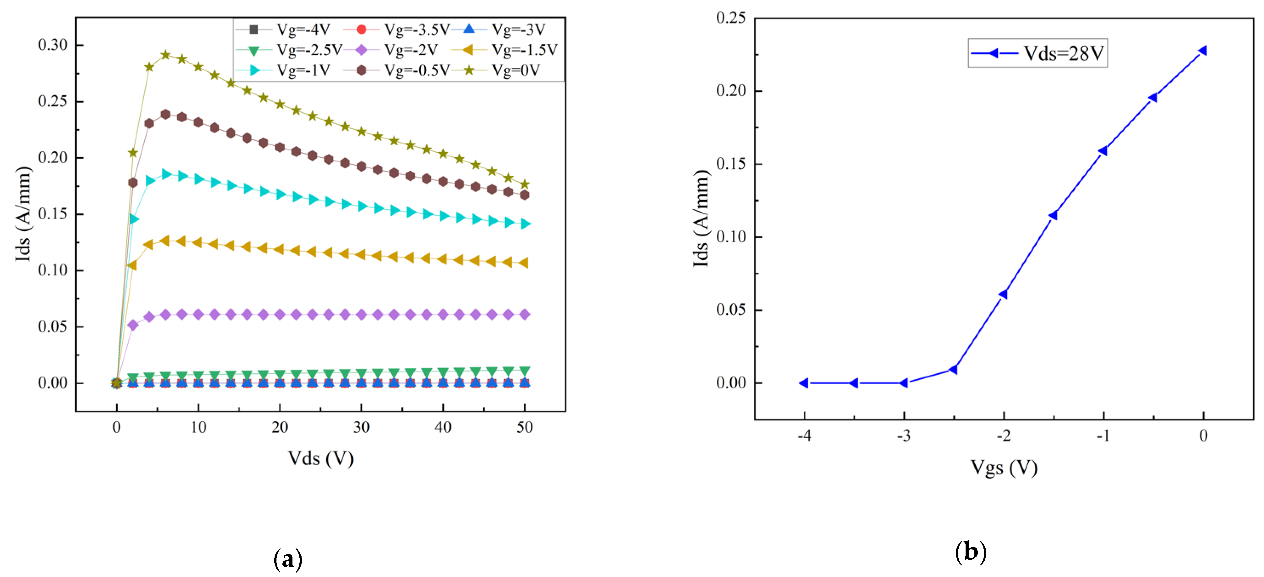
2. The 0.25 μm GaN/SiCProcess

GaN process is particularly suitable for the implementation of a high-efficiency MMIC PA due to the characteristics of high power, wideband capability, high performance, and high efficiency. In this paper, a GaN/SiC HEMT process with 0.25 µm gate length on a 100–µm–thick of SiC substrates is utilized for implementation of this PA. In this process, the maximum drain biases rating of 40 volts. Cutoff frequency ( f t ) and maximum frequency ( f m a x ) of the transistors are 25 and 75 GHz, respectively. This process utilizes a source–coupled field–plate design to provide the breakdown voltage required for reliable operation at a high drain bias. This process offers two interconnected metal layers, high–reliability metal–insulator–metal (MIM) capacitors with 215 pF/mm2 density, and precision tantalum nitride (TaN) resistors with 50 Ω/square sheet, resistivity. This process provides integrated source via (ISV) transistor device model, the structure features good electrical ground from front to backside. This process also provides air bridge, back–vias and MIM capacitors with back–vias. According to the handbook of the process, the 0.25 µm gate length GaN HEMT is well-suited for high–power applications from the C–band to the Ku–band and exhibits a high degree of process maturity [8].

3. Circuit Design

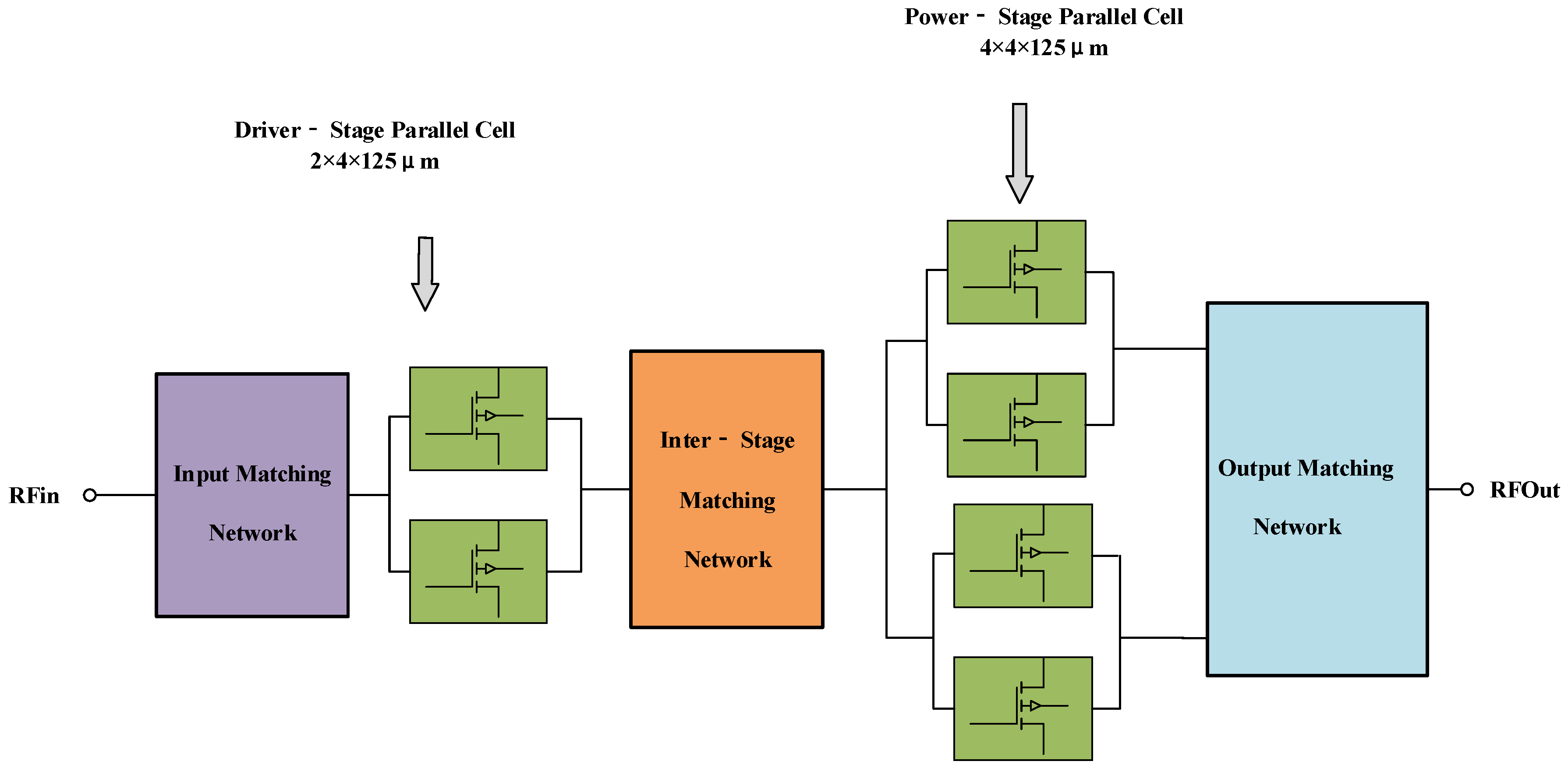
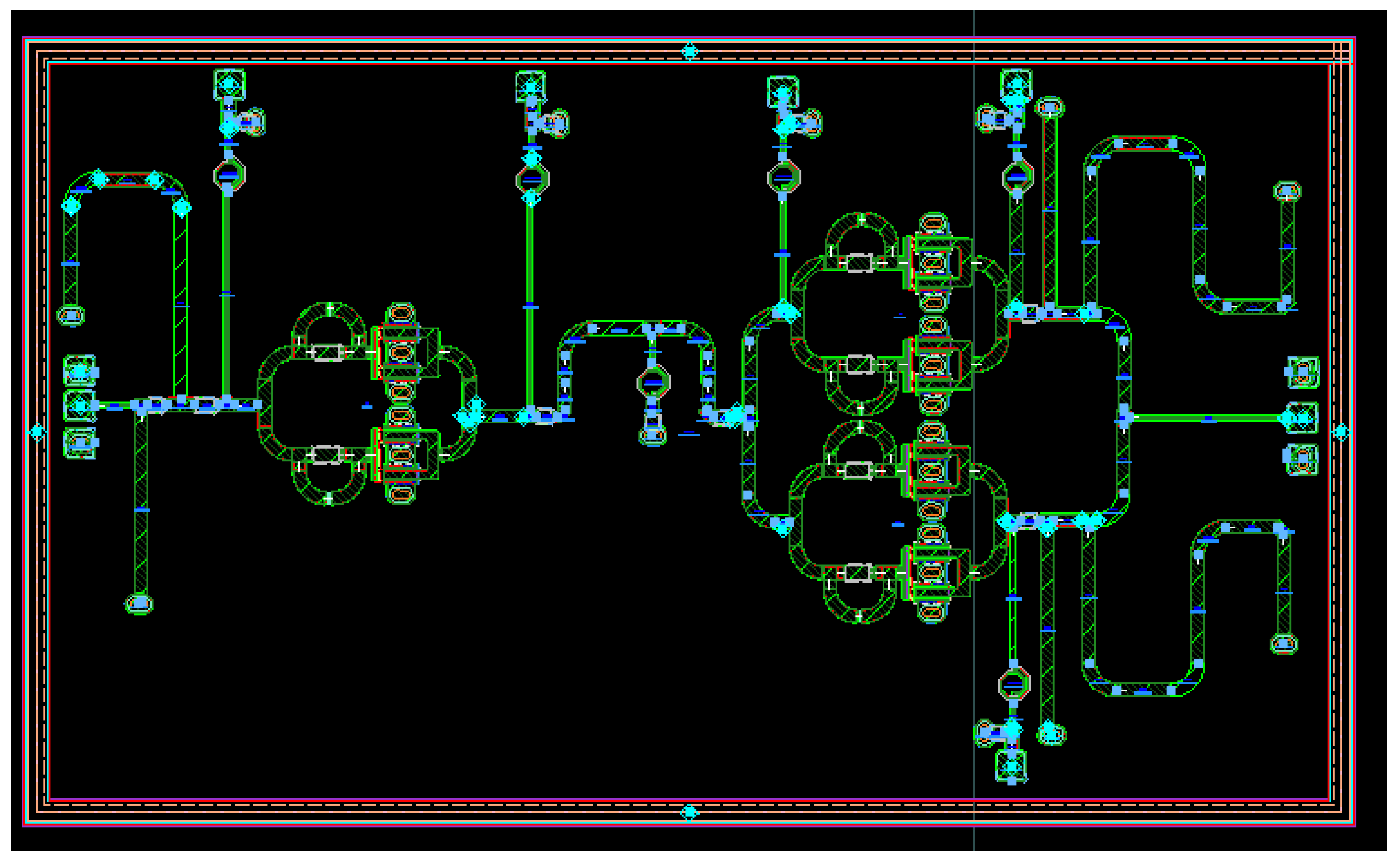
3.1. Power Amplifier Structure

The goals for this design include a 7–13 GHz bandwidth, an output power gain of 14 dB, an average P o u t of 40 dBm, and a PAE of better than 30%. The main specifications for the amplifier are summarized in Table 1.
According to Table 1, a minimum power gain of 14 dB is among the design goals of the MMIC PA. Since the maximum available gain of the chosen transistors is about 10 dB at 13 GHz, and assuming a total loss of 6 dB for the matching networks, at least two amplification stages are required.
The primary task of the power-stage transistors is to deliver the required P o u t . According to load–pull simulations biased at V g s   = −2 V and V d s = 28 V, the power density of the used transistors is about 5.6 W/mm gate width. To achieve a 40 dBm P o u t , a total transistor width of 2 mm is required. Trading off the number of fingers and the finger width, a total amount of 16 fingers is chosen and arranged as four 4 × 125 μm transistors. Figure 1a,b show the I–V curve and transfer curve (at V g s   = −2 V and V d s = 28 V) of the 4 × 125 μm device, respectively.
Moreover, the driver stage needs to provide enough linear P o u t so that the power stage can reach saturation. Simultaneously, it is also necessary to minimize the power consumption on the HEMT of the driver stage in the design to improve the overall output efficiency of the developed PA. Taking the above into consideration, we adopt two HEMT cells with a total gate width of 1 mm (2 × 4 × 125 µm GaN HEMT) for the driver stage. Moreover, the driving ratio of the multistage wideband amplifier is about 1:2, which can ensure good inter-stage matching (IMN) and broadband performance and avoid the complexity or the asymmetry in the ratios of 1:4 or 1:8 [13]. Figure 2 shows the block diagram of the proposed MMIC PA.

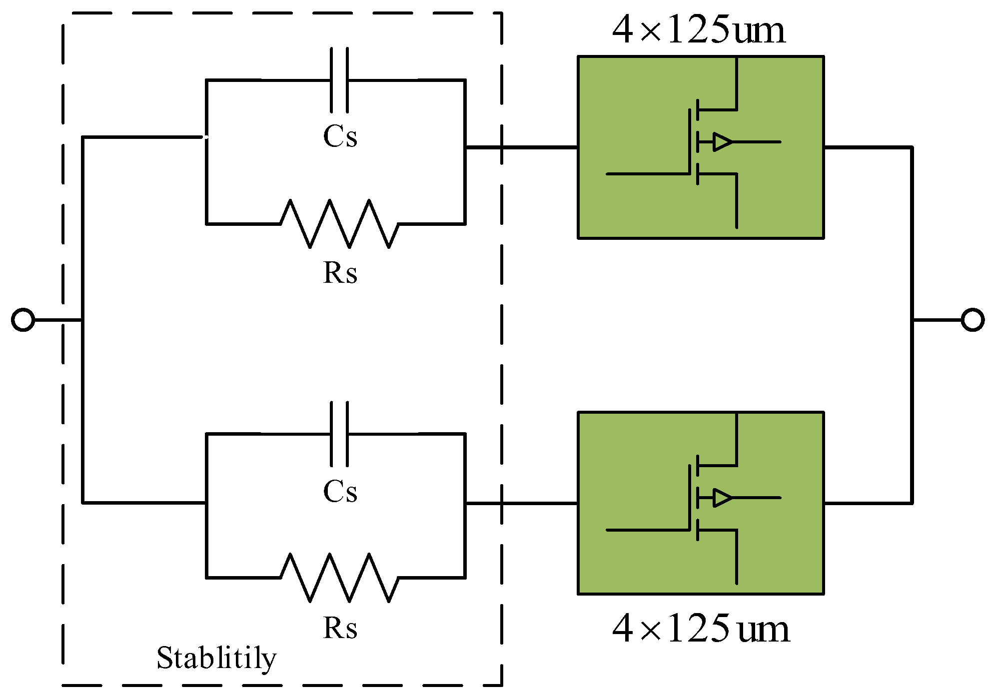
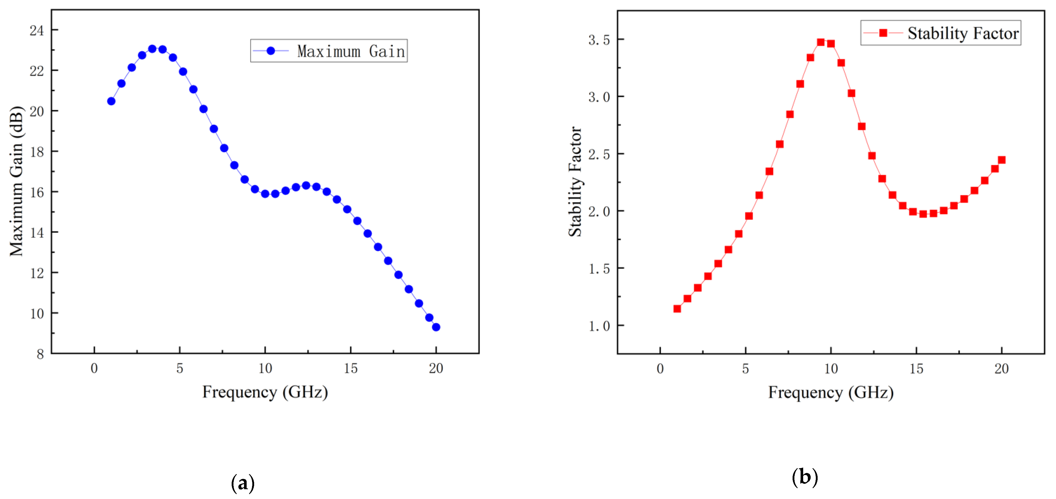
3.2. Stability Analysis and Design

The stability analysis is an essential step in this MMIC PA design. To ensure the stability of the developed MMIC PA, stability circuits were designed for each HEMT. Figure 3 shows the block diagram of the designed stability circuits. A parallel RC network, which is composed of the parallel connection of a resistance and a capacitance, is inserted at the gate of the GaN HEMT. Figure 4a,b give the simulation results of the maximum gain and stability factor, respectively. It can be seen that the simulated stability factors are higher than 1.03 throughout a frequency from 0 to 20 GHz, which confirms that the designed stability circuit can effectively improve the stability.

3.3. Broadband Design Consideration

The design of a high-efficiency power amplifier requires obtaining the optimal impedance region within the target frequency band. In this paper, we adopt the method of a load–pull simulation to obtain the optimal impedance. Table 2 gives the load–pull simulation result of the two parallel HEMTs with stability circuits for the power stage of the developed MMIC PA. These optimum impedance points are selected based on tradeoffs among the PAE, P o u t , and bandwidth. It is also observed that the optimal load impedance of the device is not constant for the whole frequency. Within the frequency range of 7–13 GHz, the P o u t and PAE are better than 37 dBm and 54%, respectively. Figure 5 gives the load–pull contours of the P o u t , PAE, and ideal load impedance at 7 and 13 GHz.
To ensure a high-frequency performance of this PA, thereby improving the gain flatness, the optimal load Z o p t is chosen to be 12 GHz. Figure 6 gives the simulation result of the P o u t and PAE versus the input power ( P i n ) at 12 GHz for a 2 × 4 × 125 µm GaN HEMT with an optimal load impedance under CW conditions. It can be seen that as the P i n increases, the P o u t gradually increases. The peak value of the PAE appears around P i n   = 27 dBm, at the same time, the P o u t also reaches a relatively high power level.

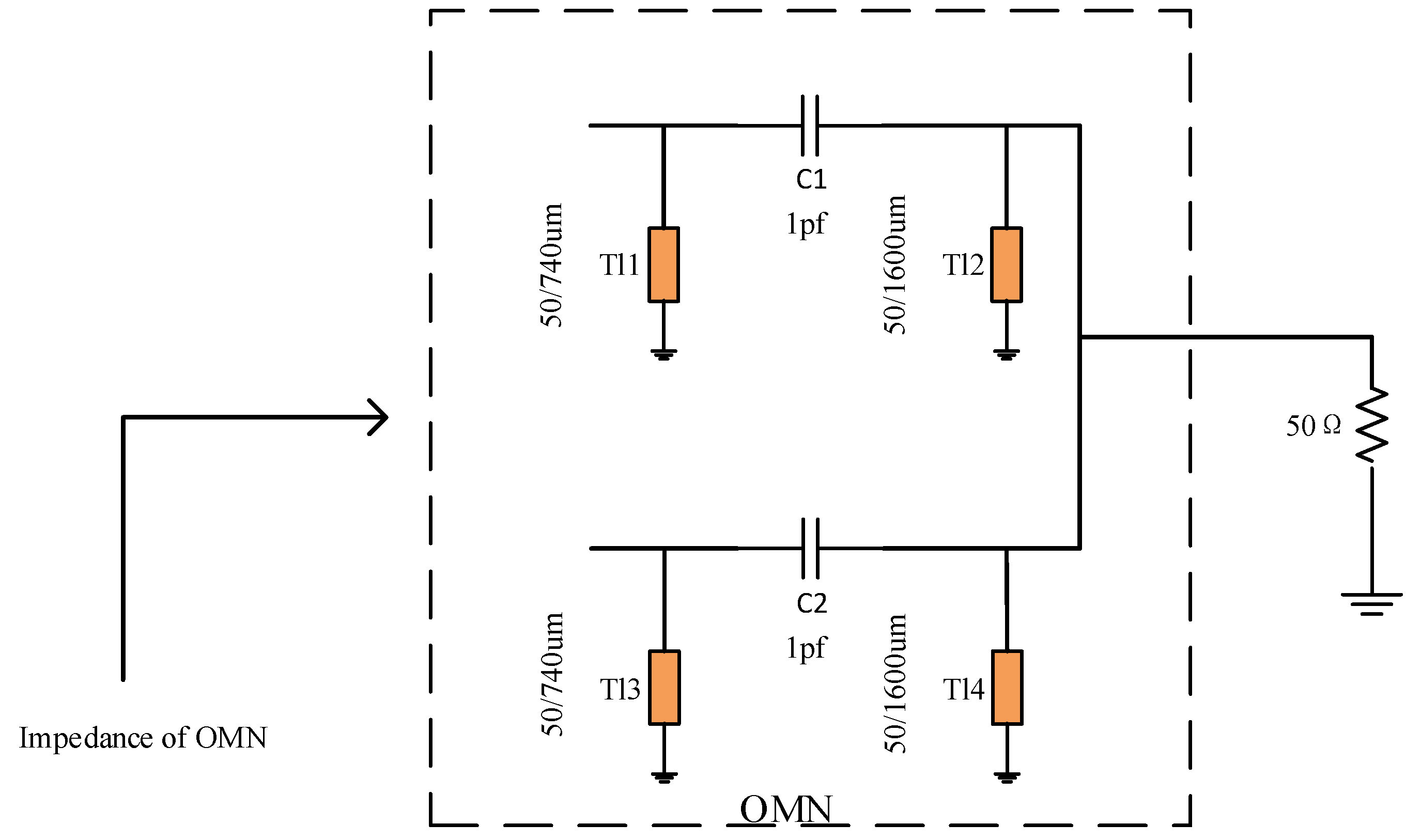
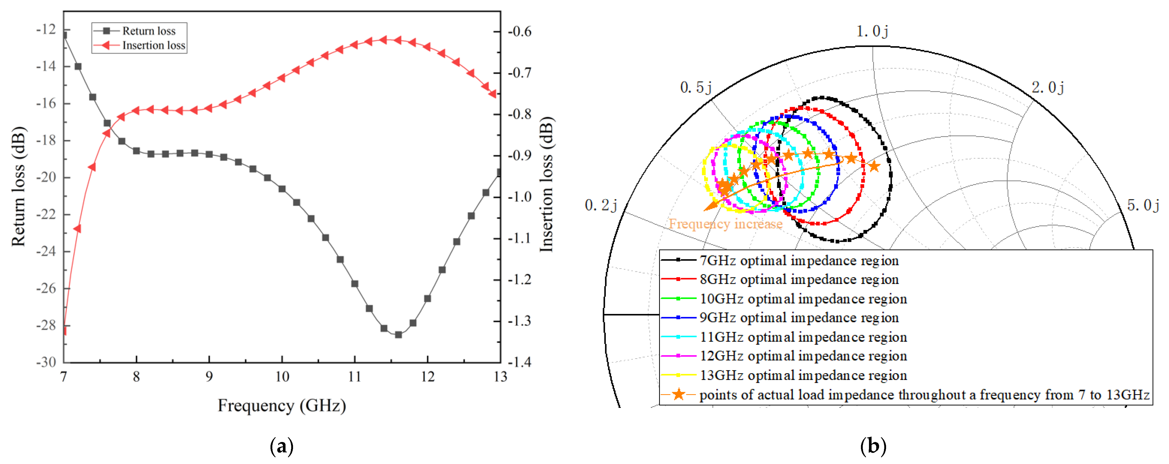
3.4. Design of Output Matching Network (OMN)

The design of the OMN needs to comprehensively consider the following five aspects [13]:
(1)
Achieve conjugate matching and attain the maximum PAE while maintaining a relatively high power;
(2)
The power transmitted by the microstrip line and the components cannot exceed its power tolerance;
(3)
Network matching should be as simple as possible to reduce losses;
(4)
The standing wave coefficient of the output terminal should not be too large, which is convenient for interconnection with external systems;
(5)
The design of the DC feeding network is reasonable.
A low-loss OMN circuit is very important for gaining a high PAE [8]. To minimize the insertion loss, the OMN circuit consists of a low-loss double-layer microstrip and a high-reliability MIM capacitor. The final topology of the proposed OMN is shown in Figure 7.
The structure of the OMN is simple; the insertion loss is reduced as much as possible on the premise of satisfying conjugate matching. The insertion loss and return loss of the OMN are shown in Figure 8a. It is seen that the loss of the output matching circuit is 1.3–0.6 dB across the frequency range of 7–13 GHz, with a return loss of better than 12 dB, which means the developed amplifier has a high efficiency and high P o u t performance. Figure 8b demonstrates the matching effect reflected by the output matching network. It can be seen that the points of actual load impedance are basically located in the optimum impedance region throughout a frequency from 7 to 13 GHz, that mean a good output matching is achieved.

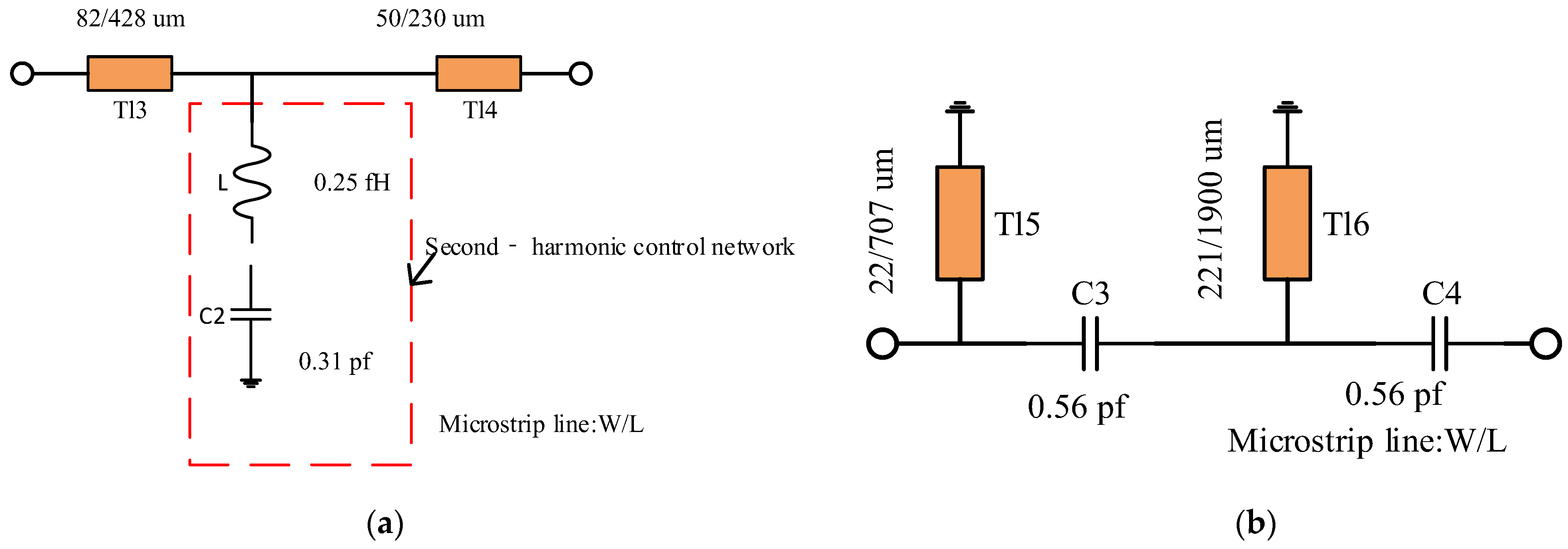
3.5. Design of Inter-Stage and Input Matching Network

There are usually two ways to design an IMN. Method 1 is by transforming Impedance A to 50 Ω and then transforming it from 50 Ω to Impedance B, and Method 2 is transforming Impedance A to Impedance B directly, as shown in Figure 9a and Figure 9b, respectively.
The advantage of Method 1 is that both Impedances A and B can be considered to be transformed from the 50 Ω standard impedance, which is relatively stable and reduces the influence of the optimal source/load impedance change caused by the change in the working state of the HEMT on the matching accuracy; the disadvantage is that the matching network will become complex, thereby increasing the chip area. The advantages of Method 2 are that Impedances A and B are directly transformed from each other, the matching network is simple, and the chip area is saved; however, the difficulty of the matching network design will also increase. After, comprehensive consideration, this design adopts Method 2 to design the IMN. Simultaneously, in order to improve the efficiency, the second-harmonic control network is used in the IMN, which is composed of an inductor and a capacitor in series. The circuit structure of the IMN is shown in Figure 10a. It can be observed that the structure of the matching network between the two stages is simple and occupies a small chip area. The design of the IMN takes into account the same factors as the design of the OMN. Figure 10b presents the structure of the proposed IMN.
The insertion loss and return loss simulation results of the ISMN are shown in Figure 11a. With a return loss better than 12 dB, the insertion loss is 1.4–0.7 dB across the frequency range of 7–13 GHz; the simulation result of the IMN is shown in Figure 11b. With a return loss better than 10 dB, the insertion loss is 2.8–1.2 dB across the frequency range of 7–13 GHz.

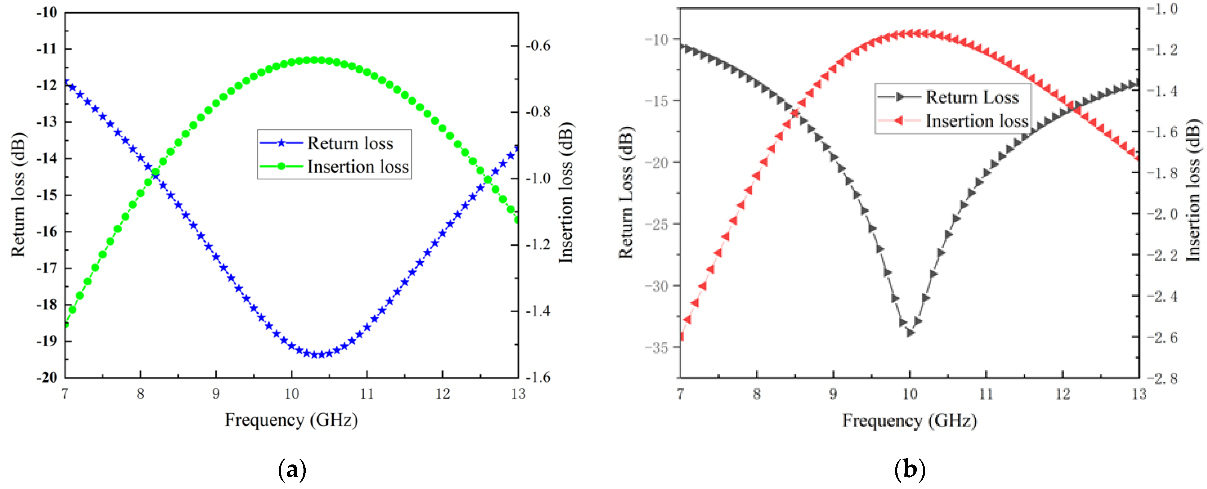
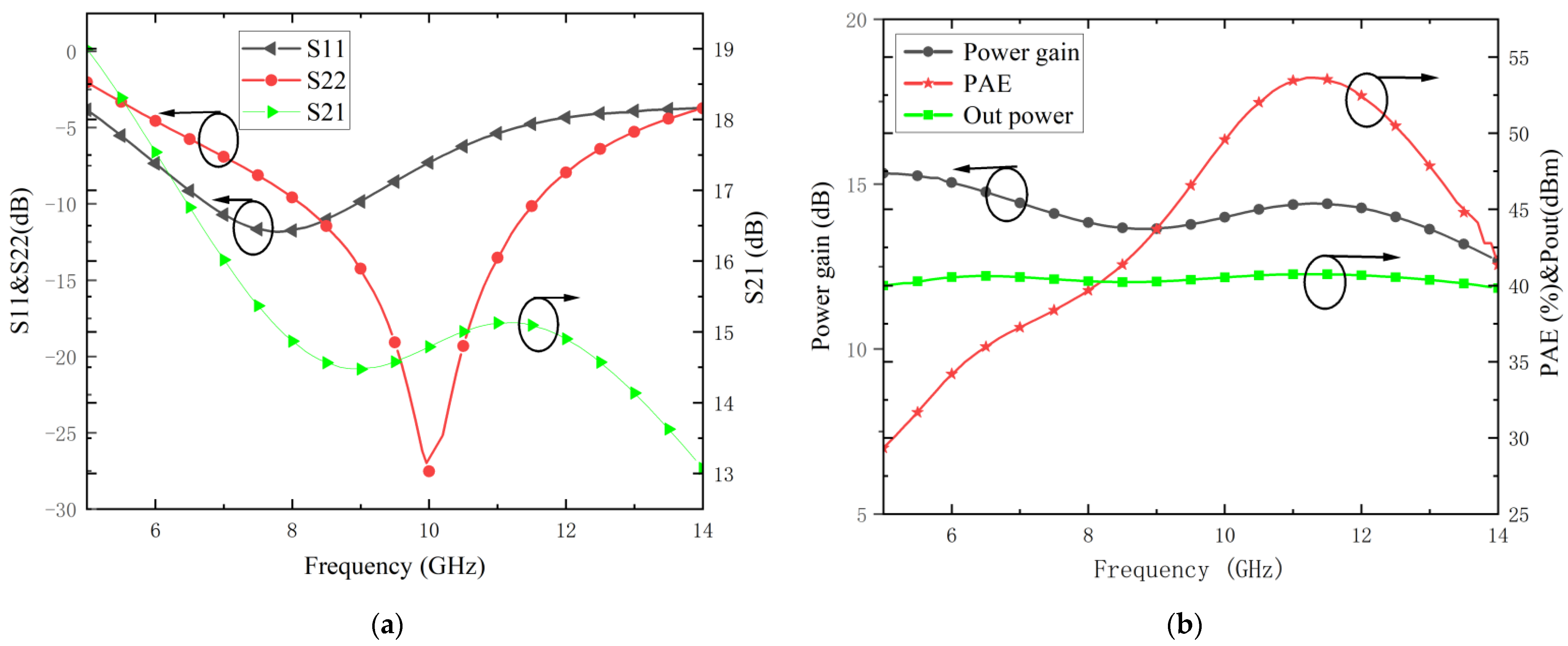
4. Power Amplifier Measurement Results

This two-stage GaN MMIC PA is implemented in a 0.25 μm gate length GaN/SiC HEMT process. Figure 12 demonstrates the final layout of the designed MMIC PA. Including the testing pads, the design occupies a size of 4.5 × 2.6 mm2.
In order to verify this design, the developed GaN PA adopts a Class-AB bias point with a drain voltage of 28 V, a gate voltage of −2 V, and a total gate current of 954 mA. The electromagnetic simulated(EM) S-parameters of the layout are shown in Figure 13a. It can be seen that in the frequency range of 7–13 GHz, the amplifier achieves a small signal gain of 14.5–15.5 dB with a gain flatness of less than ±1 dB, and the input and output return loss are better than 5 dB and 8 dB, respectively. Moreover, the simulated PAE and P o u t results of the large signal are illustrated in Figure 13b. The designed MMIC PA achieves a PAE of 30–46% with an P o u t of 40 dBm over the entire 7–13 GHz bandwidth.
In order to evaluate this MMIC PA, the performance comparison with the previously reported GaN PAs is presented in Table 3. It is obvious that the proposed PA exhibits quite a superior performance, including a high efficiency, high P o u t , and wide bandwidth in the MMIC power amplifiers.

5. Conclusions

In this paper, a 7–13 GHz high-efficiency MMIC PA design methodology and its experimental results have been presented. The designed amplifier, with a compact chip area of 4.5 × 2.6 mm2, attains an average P o u t of 40 dBm, an average power gain of 14 dB, and a PAE of 30–46%, and the input and output return losses are better than 5 dB and 8 dB, respectively, over the entire 7–13 GHz bandwidth.

Author Contributions

Data curation, A.H. and T.L.; Investigation, A.H. and T.L.; Methodology, A.H., Y.L., X.Q., T.L. and Y.P.; Project administration, Y.L. and X.Q.; Resources, Y.L. and X.Q.; Software, A.H.; Writing—original draft, A.H.; Writing—review and editing, A.H., Y.L., X.Q., T.L. and Y.P. All authors have read and agreed to the published version of the manuscript.

Funding

This research is supported by the National Natural Science Foundation of China under Grant No. 61971414; the Henan Province Key R&D and Promotion Project (Science and Technology Research) No. 212102210027; and the Zhengzhou Zhongke Institute of Integrated Circuit and System Application Research Dean Fund No. ZK2005BN003.

Institutional Review Board Statement

Not applicable.

Informed Consent Statement

Not applicable.

Data Availability Statement

The data may be obtained from the authors upon request.

Conflicts of Interest

The authors declare no conflict of interest.

References

  1. Oreja-Gigorro, E.; Delgado Pascual, E.; Sanchez-Martinez, J.J.; Gil-Heras, M.L.; Bueno-Fernandez, V.; Bodalo-Marquez, A.; Grajal, J. A 6–18 GHz GaN on SiC High Power Amplifier MMIC for Electronic Warfare. In Proceedings of the 2018 13th European Microwave Integrated Circuits Conference (EuMIC), Madrid, Spain, 23–25 September 2018; pp. 85–88. [Google Scholar] [CrossRef]
  2. Couturier, A.M.; Poitrenaud, N.; Serru, V.; Dionisio, R.; Fontecavc, J.J.; Camiade, M. 50% High Efficiency X-Band GaN MMIC Amplifier for Space Applications. In Proceedings of the 2018 48th European Microwave Conference (EuMC), Madrid, Spain, 23–27 September 2018; pp. 352–355. [Google Scholar] [CrossRef]
  3. Ye, W.; Ma, K.; Yeo, K.S. 2.5 A 2-to-6 GHz Class-AB power amplifier with 28.4% PAE in 65 nm CMOS supporting 256 QAM. In Proceedings of the 2015 IEEE International Solid-State Circuits Conference—(ISSCC) Digest of Technical Papers, San Francisco, CA, USA, 22–26 February 2015; pp. 1–3. [Google Scholar] [CrossRef]
  4. Ezzeddine, B.A.; Hung, H.A.; Viveiros, E.; Huang, H.-C. High-power GaN MMIC PA Over 40–4000MHz. In Proceedings of the 2013 IEEE MTT-S International Microwave Symposium Digest (MTT), Seattle, WA, USA, 2–7 June 2013; pp. 1–4. [Google Scholar] [CrossRef]
  5. Schellenberg, J.M. A 2-W W-Band GaN Traveling-Wave Amplifier With 25-GHz Bandwidth. IEEE Trans. Microw. Theory Tech. 2015, 63, 2833–2840. [Google Scholar] [CrossRef]
  6. Campbell, C.F.; Nayak, S.; Ming-Yih, K.; Chen, S. Design and performance of 16–40 GHz GaN distributed power amplifier MMICs utilizing an advanced 0.15 µm GaN process. In Proceedings of the 2016 IEEE MTT-S International Microwave Symposium (IMS), San Francisco, CA, USA, 22–27 May 2016; pp. 1–4. [Google Scholar] [CrossRef]
  7. Kim, Y.; Kwon, Y. Analysis and Design of Millimeter-Wave Power Amplifier Using Stacked-FET Structure. IEEE Trans. Microw. Theory Tech. 2015, 63, 691–702. [Google Scholar] [CrossRef]
  8. Hu, L.; Liao, X.; Zhang, F.; Wu, H.; Ma, S.; Lin, Q.; Tang, X. A Wideband High-Efficiency GaN MMIC Power Amplifier for Sub-6-GHz Applications. Micromachines 2022, 13, 793. [Google Scholar] [CrossRef] [PubMed]
  9. Gustafsson, D.; Cahuana, J.C.; Kuylenstierna, D.; Angelov, I.; Rorsman, N.; Fager, C. A Wideband and Compact GaN MMIC Doherty Amplifier for Microwave Link Applications. IEEE Trans. Microw. Theory Tech. 2013, 61, 922–930. [Google Scholar] [CrossRef]
  10. Meghdadi, M.; Medi, A. Design of 6–18-GHz High-Power Amplifier in GaAs pHEMT Technology. IEEE Trans. Microw. Theory Tech. 2017, 65, 2353–2360. [Google Scholar] [CrossRef]
  11. Khan, A.; Sarbishaei, H.; Boumaiza, S. High efficiency two-stage GaN power amplifier with improved linearity. In Proceedings of the 2014 IEEE Topical Conference on Power Amplifiers for Wireless and Radio Applications (PAWR), Newport Beach, CA, USA, 19–23 January 2014; pp. 4–6. [Google Scholar]
  12. Zhuang, Y.; Zhou, J.; Huang, Y.; Chen, A. Design of a broadband high efficiency GaN power amplifier for GNSS applications. In Proceedings of the 2016 IEEE MTT-S International Wireless Symposium (IWS), Shanghai, China, 14–16 March 2016; pp. 1–4. [Google Scholar]
  13. Lin, Q.; Wu, H.-F.; Hua, Y.-N.; Chen, Y.-J.; Hu, L.-L.; Liu, L.-S.; Chen, S.-J. A 2–20-GHz 10-W High-Efficiency GaN Power Amplifier Using Reactive Matching Technique. IEEE Trans. Microw. Theory Tech. 2020, 68, 3148–3158. [Google Scholar] [CrossRef]
  14. Campbell, C.F.; Balistreri, A.; Kao, M.-Y.; Dumka, D.C.; Hitt, J. GaN Takes the Lead. IEEE Microw. Mag. 2012, 13, 44–53. [Google Scholar] [CrossRef]
  15. Pengelly, R.S.; Wood, S.M.; Milligan, J.W.; Sheppard, S.T.; Pribble, W.L. A Review of GaN on SiC High Electron-Mobility Power Transistors and MMICs. IEEE Trans. Microw. Theory Tech. 2012, 60, 1764–1783. [Google Scholar] [CrossRef]
  16. X-Band 10 W MMIC High-Gain Power Amplifier with up to 60% PAE. Available online: https://www.zhangqiaokeyan.com/open-access_resources_thesis/0100060693390.html (accessed on 6 October 2022).
  17. Van Heijningen, M.; de Hek, P.; Dourlens, C.; Fellon, P.; Adamiuk, G.; Ayllon, N.; van Vliet, F. C-Band Single-Chip Radar Front-End in AlGaN/GaN Technology. IEEE Trans. Microw. Theory Tech. 2017, 65, 4428–4437. [Google Scholar] [CrossRef]
  18. Liu, R.-J.; Zhu, X.-W.; Xia, J.; Chen, P.; Yu, C.; Wu, X.-L.; Chen, X. Highly Efficient Wideband GaN MMIC Doherty Power Amplifier Considering the Output Capacitor Influence of the Peaking Transistor in Class-C Operation. IEEE Trans. Circuits Syst. Regul. Pap. 2022, 69, 1932–1942. [Google Scholar] [CrossRef]
  19. Aust, M.V.; Sharma, A.K.; Fordham, O.; Grundbacher, R.; To, R.; Tsai, R.S.; Lai, R. A 2.8-W Q-Band High-Efficiency Power Amplifier. IEEE J. Solid-State Circuits 2006, 41, 2241–2247. [Google Scholar] [CrossRef]
  20. Ayad, M.; Poitrenaud, N.; Serru, V.; Camiade, M.; Gruenenpuett, J.; Riepe, K.J. A High Efficiency MMIC X-band GaN Power Amplifier. In Proceedings of the 2020 50th European Microwave Conference (EuMC), Utrecht, The Netherlands, 12–14 January 2021; pp. 788–791. [Google Scholar] [CrossRef]
  21. Tao, H.-Q.; Hong, W.; Zhang, B.; Yu, X.-M. A Compact 60W X-Band GaN HEMT Power Amplifier MMIC. IEEE Microw. Wirel. Compon. Lett. 2017, 27, 73–75. [Google Scholar] [CrossRef]
  22. Shin, D.-H.; Yom, I.-B.; Kim, D.-W. X-band GaN MMIC power amplifier for the SSPA of a SAR system. In Proceedings of the 2017 IEEE International Symposium on Radio-Frequency Integration Technology (RFIT), Seoul, Korea, 30 August–1 September 2017; pp. 93–95. [Google Scholar]
  23. Van Raay, F.; Quay, R.; Kiefer, R.; Benkhelifa, F.; Raynor, B.; Pletschen, W.; Kuri, M.; Massler, H.; Muller, S.; Dammann, M.; et al. A coplanar X-band AlGaN/GaN power amplifier MMIC on s.i. SiC substrate. IEEE Microw. Wirel. Compon. Lett. 2005, 15, 460–462. [Google Scholar] [CrossRef]
  24. Dani, A.; Coffey, M.; Popovié, Z. 4W X-band high efficiency MMIC PA with output harmonic injection. In Proceedings of the 2014 9th European Microwave Integrated Circuit Conference, Rome, Italy, 6–7 October 2014; pp. 389–392. [Google Scholar] [CrossRef]
  25. Schafer, S.; Coffey, M.; Popović, Z. X-band wireless power transfer with two-stage high-efficiency GaN PA/ rectifier. In Proceedings of the 2015 IEEE Wireless Power Transfer Conference (WPTC), Boulder, CO, USA, 13–15 May 2015; pp. 1–3. [Google Scholar] [CrossRef]
  26. Torii, T.; Imai, S.; Maehara, H.; Miyashita, M.; Kunii, T.; Morimoto, T.; Inoue, A.; Ohta, A.; Katayama, H.; Yunoue, N.; et al. 60% PAE, 30 W X-band and 33% PAE, 100 W Ku-band PAs utilizing 0.15 μm GaN HEMT technology. In Proceedings of the 2016 46th European Microwave Conference (EuMC), London, UK, 4–6 October 2016; pp. 568–571. [Google Scholar] [CrossRef]
  27. Kang, J.; Moon, J.-S. Highly efficient wideband X-band MMIC class-F power amplifier with cascode FP GaN HEMT. Electron. Lett. 2017, 53, 1207–1209. [Google Scholar] [CrossRef]
  28. Nikandish, G.; Medi, A. A Design Procedure for High-Efficiency and Compact-Size 5–10-W MMIC Power Amplifiers in GaAs pHEMT Technology. IEEE Trans. Microw. Theory Tech. 2013, 61, 2922–2933. [Google Scholar] [CrossRef]
Figure 1. The characteristics of 0.25 μm GaN HEMT: (a) I–V curve of 0.25 μm GaN HEMT; (b) transfer curve of 0.25 μm GaN HEMT.
Applsci 12 10872 g001
Figure 2. The circuit structure block diagram of the 7–13 GHz MMIC PA design.
Applsci 12 10872 g002
Figure 3. Block diagram of the stability circuits.
Applsci 12 10872 g003
Figure 4. Simulated results of stability circuits: (a) maximum gain; (b) stability factor.
Applsci 12 10872 g004
Figure 5. Load–pull contours for P o u t and PAE from 7 to 13 GHz and ideal load impedance.
Applsci 12 10872 g005
Figure 6. P o u t and PAE of 2 × 4 × 125 µm HEMT under frequency of 12 GHz.
Applsci 12 10872 g006
Figure 7. Circuit structure of the proposed OMN.
Applsci 12 10872 g007
Figure 8. Simulation result of the OMN: (a) insertion loss and return loss; (b) points of actual load impedance.
Applsci 12 10872 g008
Figure 9. Impedance transform diagram: (a) indirect change; (b) direct change.
Applsci 12 10872 g009
Figure 10. The block diagram of the circuit structure: (a) ISMN; (b) IMN.
Applsci 12 10872 g010
Figure 11. Return loss and insertion loss of the (a) ISMN; (b) IMN.
Applsci 12 10872 g011
Figure 12. Schematic diagram of the MMIC PA layout.
Applsci 12 10872 g012
Figure 13. Layout simulation results: (a) results for small signal; (b) results for large signal.
Applsci 12 10872 g013
Table 1. Requirements for 7–13 GHz MMIC PA.
Parameter S p e c i f i c a t i o n Unit
Frequency range7–13GHz
Average P o u t 40 (10)dBm (W)
PAE30%
Power gain14dB
Table 2. Load–pull simulation result of two parallel HEMTs.
Frequency (GHz) Z o p t P o u t (dBm) PAE (%)
78.25 + j18.6939.859.63
817.59 + j31.1637.5257.51
96.03 + j16.0438.6557.24
1011.51 + j22.237.3757.68
113.95 + j13.2338.3756.59
124.26 + j11.8537.5755.42
139.29 + j20.1637.5154.68
Table 3. Comparison to previously published MMIC PAs.
Ref.ProcessFrequency (GHz) P o w e r   g a i n (dB) P o u t (dBm) PAE (%)
[1]GaN6–181139.224.5
[2]GaN7.8–8.8204350
[21]GaN8–122047.5–48.740–45
[22]GaN8.8–10.41745–4638–44
[28]GaAs7.5–12.517.53930–40
This workGaN7–13144030–36%
Publisher’s Note: MDPI stays neutral with regard to jurisdictional claims in published maps and institutional affiliations.

