Abstract
In this work, we investigated the self-heating effects of annealed Ti/Al/Ni/Au ohmic contacts and two-dimensional electron gas (2DEG) in AlGaN/GaN heterostructures under strong electric field by using the short pulse current–voltage and microwave noise measurement techniques. The experimental results demonstrated that the self-heating phenomena in ohmic contacts with the increase of current may dominate over the electrical performances of 2DEG channel. Moreover, the excess noise temperature of contact resistance was found to be more than four times higher than that of 2DEG channel at the same high current density values. The results reveal the importance of self-heating of the ohmic contacts on the device performance under short-duration (only 100 ns) and low-duty-cycle (only 10−5) pulse regime.
Keywords:
Gallium nitride; AlGaN/GaN; TLM; HEMT; contact resistance; 2DEG; hot electrons; microwave noise; self-heating 1. Introduction
Gallium nitride (GaN) has many attractive properties for high-power electronics and optoelectronic applications due to a wide bandgap of ∼3.4 eV and a high electron peak velocity of cm/s achieved at high fields [1]. High-electron-mobility transistors (HEMTs) with high density (over 10 cm) two-dimensional electron gas (2DEG) formed at the interface of AlGaN barrier and GaN channel layers are also resistant to high electric fields without the breakdown of the material [2,3].
The HEMT, operating as a power amplifier or as a switch, dissipates the electric power in the conductive channel [4] and contacts [5]. Joule heating and the associated temperature increase in the transistor channel and contacts will be more intense at high currents achieved in gated [6,7] and ungated [5,8] devices. Self-heating is one of the factors limiting the operation of transistors [9] and plasmonic devices [10]. It can be mitigated by the use of high-thermal-conductivity substrates and the use of GaN–SiC hybrid material developed on SiC substrate without a GaN buffer layer [11]. The voltage drop in the contacts needs to be accounted for when the average electric field in the channel is estimated to be in an ON state of operation of the transistor or especially for the experiments on the ungated devices [12]. At high current densities, the properties of the contacts are important for transistor reliability [13,14]. Robust electrodes for high-current experiments, especially for ungated or floating gate devices, are also needed [4,15,16,17,18,19,20].
The contact resistance is usually estimated from the standard transfer length model (TLM) measurements [21,22]. The dependence of the total resistance R between two electrodes, which is a sum of and resistance of the channel , is measured versus the gap length (channel length) L between the series of the electrodes of the TLM structure. Due to the absence of a gate in the TLM structure, an electric field profile along the channel is assumed to be homogeneous and current–voltage (I–V) characteristics at low electric fields reveal the ohmicity of the contacts. The structures with H-shaped contacts, where the contact width is wider than the width of the channel, are also employed with the advantage of lower [23,24]. Therefore, the contact resistance can be obtained from low-field measurements.
At higher fields, I–V nonlinearity (the deviation from Ohm’s law) of the total resistance is observed and the increase in R versus the electric field is explained by the increase in the intensity of electron–phonon scattering in GaN [25]. This self-heating-related increase in the total resistance usually is treated as the increase in , while is treated as a constant value, estimated from the TLM measurements at low fields [12,24]. Technological efforts have been targeted at achieving an value as small as possible, and hopefully, the achieved inequality lets one neglect the role of . The dependence on temperature was investigated [26,27,28]. However, the dependence on current (and applied electric field) when the temperature of the contacts increases due to Joule heating was not investigated.
The current and the electric field in the channel are controlled by the applied voltage to the electrodes, Virtually homogeneous current and electric field are expected in the channel between electrodes (corresponds to ), and non-homogeneous distribution of the current (and the electric field), so-called current crowding phenomena, is assumed under the electrodes (corresponds to ) [29,30,31]. The qualitatively similar distribution of the current density is considered in different systems, such as organic [32] or graphene transistors [33].
At high fields, the electron temperature in GaN is higher than the lattice temperature , even for the DC-mode measurements [34]. It is well known that the Joule heating (self-heating)-related increase in is lower in pulsed experiments. Hot-electron temperature is also related to the strong electron–LO-phonon coupling in GaN and the associated hot-phonon effect [25,35]. The experiments on microwave noise thermometry conducted at nearly isothermal lattice temperatures over a wide range of electric fields show that the hot-electron temperature (and electron energy relaxation time) depends on the dissipated power and on the 2DEG density in the GaN-based heterostructures with 2DEG channels [36]. An increase in is related also to the thermal quenching phenomena, when decreases along the voltage pulse [37]. For higher electron density, especially in the bulk, self-heating is stronger; therefore, the usage of short duration pulses is required [38].
In this paper, the self-heating of annealed Ti/Al/Ni/Au contacts to the 2DEG in AlGaN/(AlN)/GaN heterostructures was investigated under pulsed electric fields ranging up to 12 kV/cm and reaching current density values up to ∼1 A/mm. For this reason the pulsed current–voltage (I–V) and microwave noise measurements of the TLM test structures were performed.
The paper is organized as follows. In Section 2, the samples’ growth and ohmic contact fabrication are described, also, the measurement techniques are explained. In Section 3, the estimation of current dependent contact resistance is explained. A significant increase in the with current was found. The change in relative to its low-field value was found to be proportional to the dissipated electric power in . In Section 4, the microwave noise measurements are presented and the noise temperatures of and are extracted, demonstrating much higher excess noise temperature in contacts than in the channel. In Section 5, the increase in was analyzed in terms of self-heating. It was found that the self-heating of is more intense than that of , resulting in a rapid increase in the ratio with the current as the main result of this work. Finally, the results are summarized.
2. Samples and Measurement Techniques
Commercial AlGaN/(AlN)/GaN HEMT structures grown along the polar c-axis using the metalorganic chemical vapor deposition (MOCVD) method were selected for this study. The detailed description of the growth and characterization of alike structures can be found elsewhere [39,40]. In particular, layers for the AlGaN/AlN/GaN sample were grown on a 500 μm thick 6H-polytype SiC substrate as follows: a 90 nm thick AlN nucleation layer, a 1300 nmthick high resistivity GaN:C buffer, a 900 nm thick UID GaN layer and a 0.8 nm thick AlN spacer. Then, a 19 nm thick AlGaN barrier layer was grown capping it with a 2 nm thick GaN and a 1 nm thick SiN passivation layers. A similar structures, but without an AlN spacer (AlGaN/GaN) was developed on a semi-insulating 4H-polytype SiC substrate where a nominally undoped 20 nm thick AlGaN barrier and 2.5 m thick GaN buffer were capped by a 1.5 nm thick GaN layer. Figure 1b illustrates only top part of the unintentionally doped (UID) GaN layer and AlGaN barrier required for 2DEG formation.
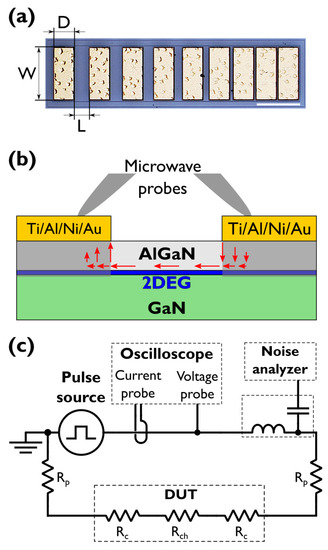
Figure 1.
Microscope image of the TLM samples of the AlGaN/GaN channel with electrodes (of width W and length D) (a) and intersection illustration of the AlGaN/GaN heterostructure with the 2DEG channel, showing the active part of the epitaxial structure and involving only two electrodes (b). Arrows illustrate the current flow. An illustration of the DUT connection in the electronic scheme is presented in (c).
The ohmic contacts were fabricated of a Ti/Al/Ni/Au metal stack with a respective thickness of 30/90/20/100 nm annealed in nitrogen ambient for 30 s at 850 °C. The mesas were formed either by inductively coupled plasma reactive ion etching (ICP-RIE) using Cl plasma or by implantation of 700 keV energy Al ions into a depth of about 650 nm. More details about the device processing have been reported elsewhere [11,41]. The TLMs were used to evaluate the performance of ohmic contacts [22]. Values for the contact resistance and specific contact resistivity at low electric fields were minimized to 1 mm and 2 mm, respectively, [11,41,42]. The Hall effect experiments in Van der Paw geometry at temperature of 300 K revealed the density and mobility values of 2DEG in used samples to be of 8.3 × 10 cm and 9.3 × 10 cm and of 1.9 × 10 cm/Vs and 1.9×10 cm/Vs, respectively.
Usually, GaN device fabrication is completed with the deposition of dielectric layers to passivate the surface states minimizing their influence on the device/transistor performance [43]. However, good performance of unpassivated HEMTs has also been reported [44,45], exposing issues of the selection and usage of the surface passivants which might deteriorate the performance. In this work, the surfaces of all heterostructures after device processing were left unpassivated.
A microscope photograph of the TLM samples, an illustration of the cross-section of AlGaN/GaN heterostructures with two metal contacts annealed on the surface, and the connection between the sample (device under test (DUT)) in the electronic scheme are shown in Figure 1a–c, respectively. The 2DEG channel formed at the interface of the AlGaN and GaN layers is indicated by the blue line. Different length channels are selected for the pulsed I–V and microwave noise measurements by placing the two-pin microwave probe on top of the selected two nearby electrodes. The width W and the length D of rectangular electrodes were 250 m and 100 m, respectively. The distance between electrodes L for different TLM resistor samples were 6, 12.5, 25, 35, 45, 55, and 65 m. We assumed that the length of the 2DEG channel is the same as L and is independent of the applied voltage. The current distribution under the right-hand side and left-hand side electrodes is considered to be the same. The current crowding phenomena is illustrated by the set of arrows (vectors which roughly show the direction and the magnitude of the current flow) parallel and perpendicular to the plane of 2DEG.
The current–voltage characteristics were measured by applying voltage pulses of width = 100 ns and a duty cycle . The current–voltage and the hot-electron noise temperature–voltage characteristics were measured by applying voltage pulses to the TLM samples with electric field values reaching up to ∼12 kV/cm.
A voltage pulse generator (Generator AVL-2A-W-B-P-M, Avtech Electrosystems) was connected to the DUT through a coaxial current probe, a coaxial voltage probe, a microwave diplexer, and a microwave probe (Model 40A with a two-pin ground-signal configuration, 100 m pitch, GGB Industries), which was mounted on a high-precision probe station with vibration isolation (EPS150, Cascade Microtech). The coaxial voltage probe was realized as a pick-off tee giving 30 times attenuated replica of the voltage pulse. The coaxial current probe (Model 6027, Pearson Electronics) was inductively coupled giving the voltage replica of the current pulse (conversion ratio 1 Volt/Ampere). Signals from both probes were recorded by a digital oscilloscope (DSO1022A, Keysight Technologies).
As the DUT is biased by the voltage pulse, the excess microwave noise (where is noise temperature and is room temperature) of the DUT appears at the pins of the microwave coaxial probe. The microwave diplexer is used to route the microwave noise of the DUT to a noise analyzer, consisting of low-noise amplifiers, a diode detector, and a box-car averager with a gating function (SR250 with modules 240A, 245, Stanford Research Systems). The diplexer was connected in the close vicinity to the DUT; it was connected straight to the coaxial connector of the coaxial microwave (two-pin) probe. The total resistance of the DUT is a sum of contacts resistances and the resistance of the channel, , while is the resistance of the connections between the voltage probe and the DUT, including the resistance of the microwave probe. The description of experimental setups can be found elsewhere [46,47]. In microwave noise temperature experiments, the module of complex parameter (i.e., reflection coefficient in pulsed mode) of the DUT at ∼10 GHz also was measured and used for the proper estimation of the noise temperature [48,49].
Mesa-isolated TLM electrodes (i.e., channel etched) were used for the leakage current test and for standard parameter spectra measurements by vector network analyzer operating up to 40 GHz. Extracted parasitic capacitance (parallel to the channel) for the shortest channel was less than ∼50 fF. From spectra measurements of normal TLM structures (i.e., channel not etched), a small serial inductance ∼30 pH was extracted.
The results of the low-field total resistance measurements of the three heterostructure samples (with and without an AlN thin barrier layer) in the TLM configuration are shown in Figure 2. TLM measurements were conducted with conventional contact-front (two-terminal) method [22]. The total resistance of the DUT is the sum of the channel resistance and contact resistance (see Figure 1c):
where the resistance of the 2DEG channel (layer) is expressed in terms of sheet resistance of the 2DEG channel between electrodes [22]. If the length L is reduced to zero, the total resistance approaches 2. The contact resistance can be expressed as:
where is the sheet resistance of the 2DEG channel directly under the electrodes and is a transfer length [50], which is assumed to be in our work. Measured total resistance of different length TLM samples (symbols in Figure 2) was fitted by Equation (1) (lines) and both resistances, and , were extracted. The interception of lines with the abscissa axis gives and the interception with ordinate axis is [50]:
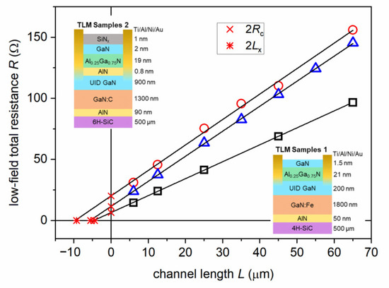
Figure 2.
The dependence of the low-field total resistance R on the channel length L. Data for group of TLM samples 1, fabricated of AlGaN/GaN (bottom inset), are shown by rectangles, meanwhile, the triangles as well as circles demonstrate results for other two groups of TLM samples 2, made of AlGaN/AlN/GaN (top inset).
The total resistance dependencies on the current are shown in Figure 3a. At the current region up to ∼50–100 mA, R weakly depends on current, which corresponds to the Ohm’s law region. The corresponding electric field range (i.e., low-field range) is up to 1–2 kV/cm. This also means that the contact resistance and channel resistance are both ohmic at this region. A deviation from Ohm’s law (an increase in R) is observed when the current and electric field become higher than ∼100 mA and ∼2 kV/cm, respectively. Maximal applied voltages for each length channel are indicated in Figure 3a. Those voltages correspond to an electric field in the channels in excess of 10 kV/cm. This nonlinear electron transport phenomena in the AlGaN/GaN channels is explained by the increase in intensity of electron–phonon scattering at higher fields [25]. This is described as a decrease in field-dependent electron drift mobility , which enters a simple relation where is the sheet electron density. Unexpectedly, at high currents the total resistance for the shorter channels increases more steeply and thus, the ratio decreases with current when channel lengths (Figure 3a). Particularly, near Ohm’s region, the ratio for longest to shortest channel is ∼6.5, while at 270 mA it is ∼4.8. According to Equation (1), the change (decrease) in the ratio with current means that the ratio depends (increases) on current. It is worth noting that in most of the experiments, an independent contact resistance on the current density (with a constant value of ) is assumed. However, a contact resistance vs. current dependence, , should be considered by using a procedure that is illustrated in Figure 3.
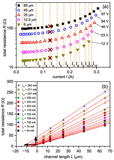
Figure 3.
The dependence of the total resistance R on the current I for the different channel length L (a) and on channel length for a different current (b). L = 6 m (closed triangles), 12.5 m (open diamonds), 25 m (open triangles), 45 m (open circles) and 65 m (closed rectangles). The measurements are presented for the AlGaN/GaN channel. The resistance values at a given currents (represented by the vertical dashed lines) are obtained from a linear interpolation; for the particular current I = 126 mA those are indicated as crosses. The applied maximal voltage for each length channel is indicated in the right side of the figure. Interpolated values of different length channels are depicted in the (b) for each current and are used for the estimation of the current dependent contact resistance and (see interception with abscissa and ordinate axis in (b)). Solid lines are linearly fit with Equation (1) and arrows show the direction of the increase in and . I = 24 mA, 74 mA, 100 mA, 126 mA, 153 mA, 178 mA, 203 mA, 220 mA, 236 mA, 257 mA, 271 mA and 282 mA.
3. Current-Dependent Contact Resistance
In this work, the contact resistance is defined as:
where is the low-field (at Ohm’s law region) contact resistance and represents the change in contact resistance over its low-field value.
Because of the dependence of R on the bias, the plot should be taken at a constant bias in contrast to Figure 2, where any bias for different L channels could be taken until measurements are done in Ohm’s region. It is convenient to use a constant current for an plot because the current is a good quantity to compare the different length channels; the same current in a different L implies that the electric field also will be the same in those channels. The data points in Figure 3a are not horizontally aligned because the pulsed voltage generator is not an ideal current source but is rather a voltage source with some internal resistance. Linear interpolation between experimental points was used so that R values at constant I (see vertical lines) could be compared. Crosses in Figure 3a illustrate the procedure for a case when I = 126 mA. The characteristics obtained in this manner are shown in Figure 3b.
It is worth mentioning that the contact resistance was assumed to be the same for all electrodes of the TLM samples. This assumption also allows for the observation of linear characteristics shown in Figure 2 and Figure 3b. An increase in and with an increase in I are observed as indicated in Figure 3b by the vertical arrow and the horizontal arrow, respectively.
The and dependencies on the current density for three samples are depicted in Figure 4a. Here, and values were multiplied by contact width W = 250 m and the current I values were divided by W.
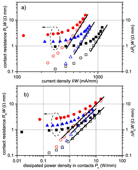
Figure 4.
The dependence of the contact resistance on the current density (a) and on the dissipated electric power density in contacts (b) for different samples; AlGaN/GaN (squares), AlGaN/AlN/GaN (triangles and circles). The dependence of the contact resistance change relatively to its low-field value is also presented (right-side axis). Lines are (a) and (b), respectively.
At low currents, where Ohm’s law holds, weakly depends on the current and . For smaller (rectangles), the increase in is slower. Roughly in the range of the measured currents, increases by more than six times as the current exceeds ∼1 A/mm (closed rectangles). The same increase (approximately six times, circles) for the sample of higher is reached at ∼0.6 A/mm.
The dependence is nonlinear and develops a steep increase which approaches and exceeds (see lines in Figure 4a) at highest currents. This fast increase in at a high current suggests that, even for very small values, a noticeable increase in can be expected at high currents. The dependence of and on the electric power density dissipated in the contact resistances is presented in Figure 4b. It is found that in the wide range of , from ∼0.5–1 W/mm to ≳10 W/mm (see the lines in Figure 4b).
The dependence of on I, which is obtained similarly to the in Figure 3 (but from the interception with the ordinate axis) is depicted in Figure 5. The dependencies are qualitatively similar to those of in Figure 4. Furthermore, the increasing can thus approach or even exceed some channel lengths used in this work (see Figure 5, circles).
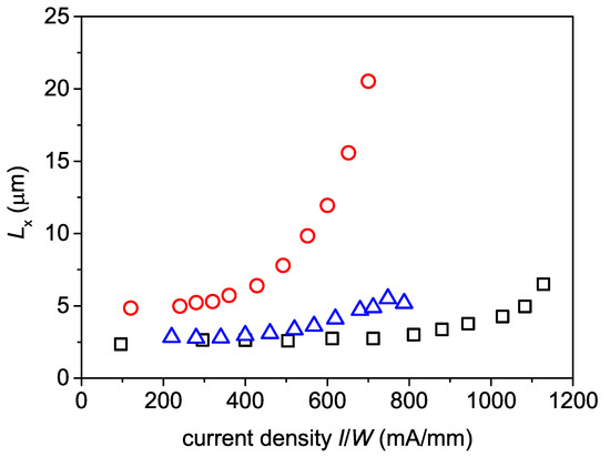
Figure 5.
The dependence of on the current density for different samples; AlGaN/GaN (squares), AlGaN/AlN/GaN (triangles and circles).
4. Noise Performance of and
Next, we proceed with the noise measurements, the results of which are shown in Figure 6. Higher excess noise temperature is obtained for the shorter channel (Figure 6a, closed triangles).
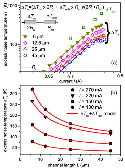
Figure 6.
The dependence of the microwave excess noise temperature on the current for the different channels length of the same TLM in the AlGaN/GaN sample (a). L = 6 m (closed triangles), 12.5 m (open diamonds), 25 m (open triangles) and 45 m (open circles). Lines guide the eyes. Estimated at the constant currents is plotted versus channel length (b). I = 100 mA (circles), 150 mA (rectangles), 220 mA (triangles) and 270 mA (pentagons). Curves are the fit by the model (Equation (6)). Excess noise temperature of the contact resistance is estimated as a fitting parameter and its current dependence is depicted by the open rectangles.
The excess noise temperature taken at constant currents for the different length channels is depicted in Figure 6b (symbols). The decrease in can be explained by the presence of two distinct noise temperatures and in the sample where the former is that of the contact resistances and the latter is that of the channel resistance . It is easy to show that of the serial connection of and is:
It follows that if , then decreases from to , as the ratio decreases from infinity to zero, while both temperatures , and do not depend on L at a given current and only depends on L. Thus, the measured dependence can be used to extract the temperatures and by fitting the experimental data with:
where and are known (see Figure 3b). The solid curves in Figure 6b are the fit with the (, ) model (Equation (6)). Formally small signal resistances at ∼10 GHz should be used in Equation (6); however, this simple model gives a good qualitative picture of two different noise temperatures: the noise temperature of is higher than that of the channel resistance. The extracted is indicated by the squares in Figure 6a.
5. Discussion
The increase in the contact resistance with the current can be treated in terms of self-heating. The nearly linear dependence of on dissipated power density is obtained in Figure 4b. In fact, the dissipated power in the contacts controls the change in , which is evident from Figure 7, where the relative contact resistance change is plotted. The dependencies of different samples almost coincide when they are plotted versus .
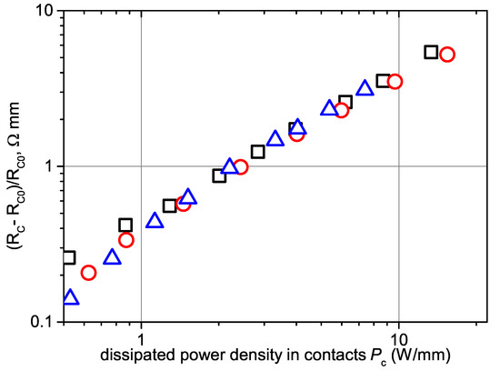
Figure 7.
The dependence of the relative contact resistance change on the dissipated electric power density in contacts for different samples; AlGaN/GaN (squares), AlGaN/AlN/GaN (triangles and circles).
Self-heating of the contact resistance also follows from the noise experiment (see Figure 6) under the assumption that noise temperature is a measure of electron gas temperature in the contact resistance, i.e. . The excess noise temperature of contact resistance (squares) approaches ∼700 K.
The assumption is realistic because it is based on the experiments with the GaN-based 2DEG channels, where the microwave noise temperature of hot electrons is approximately equal to hot-electron temperature [51].
The dependence of channel resistance change on dissipated power density in the channel is presented in Figure 8 (closed symbols). It was found, that qualitatively, the change in contact and channel resistances is similar and follows a linear trend at higher power in both cases (see open symbols in Figure 4b and Figure 8, respectively).
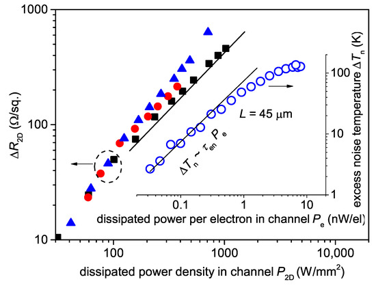
Figure 8.
The dependence of channel resistance change on dissipated power density in channel; AlGaN/GaN (closed squares), AlGaN/AlN/GaN (closed triangles and circles). The inset shows the dependence of the excess noise temperature on the dissipated power per electron in the 45 m-long channel. The lines in the main panel and inset demonstrate the dependencies of and , respectively.
The contact resistance can be described as [50]:
where is the specific contact resistance. In actuality, is the resistance from the metal to 2DEG under the electrodes. In Figure 1b, the current flow in and is shown as vertical and horizontal current vectors (in shaded areas only), respectively.
Therefore, the observed self-heating of is related with the self-heating of both resistances and . The contact-end (three-terminal) measurement method was developed for the estimation of the and values [22,50]. The contact-front (two-terminal in this work) measurements, which are standard measurements of TLM, assume that . The specific resistance obtained by contact-front method are denoted here as . It was found that and the temperature dependencies of and were qualitatively different [52]. Disregarding those concerns, was estimated and the results are shown in the inset of Figure 9. If we assume that the properties of the channel under the electrodes are similar to those between the electrodes (), then the contact-front and contact-end methods give the same results, i.e., and .
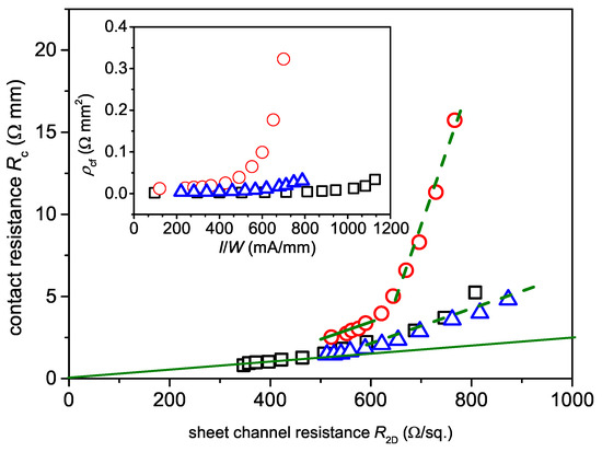
Figure 9.
The dependence of the contact resistance on the channel sheet resistance for different samples; AlGaN/GaN (squares), AlGaN/AlN/GaN (triangles and circles). Lines illustrate the slopes of the dependencies. Starting at 750 /sq., the increase in becomes faster (dashed lines versus solid lines).
Reiterating, in the present work, , , and increase with an increase in the current, while and are not known with confidence.
We also can consider an unintentionally formed field-plate-like structure near electrode, which, at higher voltages in the channel, could induce a local high-resistance region near the edge of electrode which also would appear as a increase in R. In this case, the open symbols in Figure 4a would correspond to the resistance of the high-resistance region and not to the contact resistance change. However, it would be difficult to explain why this resistance is so different (more than 10 times), as it is compared between three channels at a given current.
An interesting correlation is observed in the dependencies of (inset of Figure 9) and (Figure 4) on the current for different samples. In that case the increase in both starts earlier if low-field resistance is higher. For example, from Figure 4a it follows that the difference of between two samples (closed squares and circles) is ∼3 times, and that correlates with more than ∼12 times difference in at an elevated current density of ∼700 mA/mm (Figure 4a). This makes sense, because is higher for larger at the same current, resulting in an increase in self-heating.
In other experiments, when the change in sample temperature was realized by direct heating of the sample (instead of Joule heating), two distinct trends of the change in and versus temperature were found [26,27,28,52,53,54,55,56,57,58,59]. The decrease in was attributed to the metal–semiconductor junction properties and the increase was due to metal-like behavior when electron transport is determined by the “spike mechanism”—metal protrusions directly contacting the 2DEG channel under the electrodes
As it was previously discussed, both and increase due to self-heating (Figure 4 and Figure 8). This is also observed in Figure 3a, where the dependence of the total resistance on the current is nonlinear. In terms of sheet resistance , an increase is observed in Figure 3b, where the slope (which is proportional to ) changes with the current. The increase in the resistance of the 2DEG channel at the interface of AlGaN and GaN is widely acknowledged to be due to electron–phonon scattering, the intensity of which increases with the temperature of the device at a high current. The electron scattering is largely determined by the strong electron-LO–phonon interaction in the GaN and associated hot-phonon effect [25].
It is natural to expect that the 2DEG channel properties of the area beneath the electrodes (which have a sheet resistance of ) at least in part would preserve some features of the channel between the electrodes (which have a sheet resistance of ). Therefore, we compare the self-heating of and by plotting versus in Figure 9. Here, is multiplied by W as in Figure 4. The channel sheet resistance is estimated from the slope (see Figure 3b) and the channel width W as . In Figure 9, is nearly proportional to at lower currents (see solid lines), but then, it starts to increase faster than (see dashed lines). The threshold-like increase in is resolved, revealing the threshold position for all three samples at value of about ∼600 /sq.
The increase in is not good news for those who fabricate devices with small and those who believe that it will remain the same small at higher currents (electric fields). The situation is even more dramatic, because the ratio (and ) also increases with the current. Indeed, from Figure 9 it can be concluded that above the threshold increases faster than . We recognize that this is the most important result of the present work. This behavior has many practical consequences, because a fast increase in depending on I can deteriorate the performance of electronic devices.
The increase in the ratio can be discussed in terms of stronger self-heating compared to that of . Excess noise temperature in (Figure 6, squares) is more than four times stronger than in the total resistance R of 45 m-long channel (circles). The term in Equation (5) is not negligible, even for the 45 m-long channel (it would be negligible for the infinitely long channel only). Therefore, of a 45 m-long channel reaches ∼130 K at a ∼0.3 A, and it is still slightly higher than its . Thus, the relation holds. This suggests that the temperature (and thus, the self-heating) of is higher than the temperature of .
Let us first discuss the option that the self-heating of is caused by the self-heating of (see Equation (7)), while self-heating is negligible. The current density in is smaller than in , therefore, the stronger self-heating of compared to , might seem surprising. The current profile is illustrated in Figure 1b where the horizontal current vector magnitude gradually decreases as the current branches toward the electrodes. A detailed description of the current dependence on the distance can be found elsewhere [22]. We could suppose, that due to lower electron mobility or lower sheet electron density under the electrodes. In this case dissipated power per unit area at a given current density j will be higher because . Higher dissipated power in the contact resistance results in higher self-heating of . The next option is the self-heating of . If the metal-like shunt resistances from the metal to the 2DEG channel under the electrodes persists, the electron mobility in these shunt resistances is expected to be poor due to the high density of electrons and associated intensive electron–electron scattering. However, the high electron density in metals is what could make the specific resistance of those metal protrusions low. The current density in metal protrusion is high if its cross section is small, leading to high resulting values of the dissipated power density per unit volume.
The self-heating model in terms of the two temperatures and is oversimplified. In GaN-based 2DEG channels (applicable to and ), excess (hot) electron temperature is higher than the excess lattice temperature when the constant electric field is applied [34]. In the pulsed mode, is lower when compared to the DC mode; therefore, at short voltage pulses a nearly isothermal condition is maintained (), and the self-heating effects related to acoustic phonons are mitigated. Furthermore, in the pulse mode, is higher due to the thermal quenching effect when the hot-electron temperature decreases along with the voltage pulse due to the electron mobility decrease [37]; the shorter the pulse, the weaker the thermal quenching. Mainly because of lower in the pulsed mode, higher electric fields and currents can usually be reached without the thermal breakdown of the channel. It is also important to mention, that even in the pulsed mode, at higher electric fields the LO-phonon-related self-heating is present. For 2DEG densities, typical for GaN-based heterostructures, the hot-phonon effect is important, as non-equilibrium LO-phonons (hot-LO-phonons) strongly impact the hot-electron transport and temperature [25,35]. At high fields under conditions of strong hot-electron–hot-phonon coupling, when the system is strongly non-equilibrium, the hot-electron temperature is close to the effective hot-LO-phonon temperature . In this case, different temperatures , and are introduced, for which the relation holds [51]. The hot-electron excess temperature is controlled by electron energy relaxation time , , where is the dissipated power per electron and n is the electron density [60]. The dependence of excess noise temperature on dissipated power per electron in the 45 long channel is shown in the inset of Figure 8 (open circles), where N is electron number in the channel available from the Hall measurements. The line in the inset is plotted for constant in the channel. At a higher power per electron, decreases due to enhanced electron–LO-phonon scattering, and experimental points (circles) deviate from that line. If the electron mobility in the 2DEG channel under the electrodes is lower than in the 2DEG channel between electrodes (corresponding to and , respectively), then at a given current, in the former channel will be higher. Indeed, at a given current, the electric field (and thus, ) will be higher for the 2DEG channel with a lower electron mobility. A higher results in a higher (see inset of Figure 8). For the metal-like conductor, the hot-electron effect is not well expressed due to poor electron mobility; therefore, . In this case, , where is the heat capacity per unit volume. As such, qualitatively both cases (GaN-based channels and metal-like conductors) are similar in that . This is the reason why it is difficult to differentiate between the self-heating of resistances and from the temperature–current measurements. Assuming that and , the data in the inset of Figure 9 indicate the strong self-heating of .
To conclude, we investigated the pulsed current–voltage (I–V) and hot-electron microwave noise (at 10 GHz frequency) characteristics of the TLM samples composed of AlGaN/(AlN)/GaN heterostructures with annealed Ti/Al/Ni/Au ohmic contacts to the 2DEG channel. From the I–V measurements, the increase in the contact resistance dependent on the current was found for all samples, with a change up to six times as the current density approached ∼0.6 A/mm. The comparison of current dependence and the channel resistance revealed that is more sensitive to the current change. It was found that the change in from its low-field value is proportional to the electric power dissipated in the contacts. The pulsed microwave noise measurements further confirmed that the noise temperature of the contacts is notably higher when compared to the noise temperature of the channel. The increase in the contact resistance (and temperature) was interpreted as a result of self-heating.
Author Contributions
Conceptualization, E.Š. and I.K.; investigation, E.Š., J.J., A.Š., V.K. and I.K.; writing—original draft preparation, E.Š. and I.K.; writing—review and editing, E.Š. and I.K.; visualization, E.Š., J.J. and I.K.; supervision, E.Š. and I.K.; project administration, I.K.; funding acquisition, I.K. All authors have read and agreed to the published version of the manuscript.
Funding
The work was supported by the Research Council of Lithuania (Lietuvos mokslo taryba) within the framework of the “T-HP” Project (grant No. DOTSUT-184) funded by the European Regional Development Fund according to the Measure No.01.2.2-LMT-K-718-03-0096.
Institutional Review Board Statement
Not applicable.
Informed Consent Statement
Not applicable.
Data Availability Statement
The data presented in this study are available on request from the corresponding author. The data are not publicly available due to privacy.
Acknowledgments
The authors are sincerely grateful to J. Malakauskaitė and V. Jakštas for assistance in sample fabrication, to P. Prystawko for fruitful discussions of the various aspects of this work.
Conflicts of Interest
The authors declare no conflict of interest.
References
- Morkoç, H. Handbook of Nitride Semiconductors and Devices; Wiley-VCH: Weinheim, Germany, 2008. [Google Scholar] [CrossRef]
- Abid, I.; Kabouche, R.; Bougerol, C.; Pernot, J.; Masante, C.; Comyn, R.; Cordier, Y.; Medjdoub, F. High Lateral Breakdown Voltage in Thin Channel AlGaN/GaN High Electron Mobility Transistors on AlN/Sapphire Templates. Micromachines 2019, 10, 690. [Google Scholar] [CrossRef] [PubMed]
- Abid, I.; Mehta, J.; Cordier, Y.; Derluyn, J.; Degroote, S.; Miyake, H.; Medjdoub, F. AlGaN Channel High Electron Mobility Transistors with Regrown Ohmic Contacts. Electronics 2021, 10, 635. [Google Scholar] [CrossRef]
- Gonschorek, M.; Carlin, J.F.; Feltin, E.; Py, M.A.; Grandjean, N. Self heating in AlInN/AlN/GaN high power devices: Origin and impact on contact breakdown and IV characteristics. J. Appl. Phys. 2011, 109, 063720. [Google Scholar] [CrossRef]
- Kuzmík, J.; Bychikhin, S.; Pogany, D.; Gaquière, C.; Morvan, E. Current conduction and saturation mechanism in AlGaN/GaN ungated structures. J. Appl. Phys. 2006, 99, 123720. [Google Scholar] [CrossRef]
- Kuzmik, J.; Tapajna, M.; Valik, L.; Molnar, M.; Donoval, D.; Fleury, C.; Pogany, D.; Strasser, G.; Hilt, O.; Brunner, F.; et al. Self-Heating in GaN Transistors Designed for High-Power Operation. IEEE Trans. Electron Devices 2014, 61, 3429–3434. [Google Scholar] [CrossRef]
- Sarua, A.; Ji, H.F.; Kuball, M.; Uren, M.; Martin, T.; Hilton, K.; Balmer, R. Integrated micro-Raman/infrared thermography probe for monitoring of self-heating in AlGaN/GaN transistor structures. IEEE Trans. Electron Devices 2006, 53, 2438–2447. [Google Scholar] [CrossRef]
- Duffy, S.J.; Benbakhti, B.; Kalna, K.; Boucherta, M.; Zhang, W.D.; Bourzgui, N.E.; Soltani, A. Strain-Reduction Induced Rise in Channel Temperature at Ohmic Contacts of GaN HEMTs. IEEE Access 2018, 6, 42721–42728. [Google Scholar] [CrossRef]
- Ranjan, K.; Arulkumaran, S.; Ng, G.I.; Sandupatla, A. Investigation of Self-Heating Effect on DC and RF Performances in AlGaN/GaN HEMTs on CVD-Diamond. IEEE J. Electron Devices Soc. 2019, 7, 1264–1269. [Google Scholar] [CrossRef]
- Janonis, V.; Pashnev, D.; Grigelionis, I.; Korotieiev, V.; Balagula, R.M.; Minkevicius, L.; Jorudas, J.; Alexeeva, N.; Subacius, L.; Valušis, G.; et al. Electrically-pumped THz emitters based on plasma waves excitation in III-nitride structures. In Terahertz Emitters, Receivers, and Applications XI; Razeghi, M., Baranov, A.N., Eds.; SPIE: Washington, DC, USA, 2020; Volume 11499, p. 8. [Google Scholar] [CrossRef]
- Jorudas, J.; Šimukovič, A.; Dub, M.; Sakowicz, M.; Prystawko, P.; Indrišiūnas, S.; Kovalevskij, V.; Rumyantsev, S.; Knap, W.; Kašalynas, I. AlGaN/GaN on SiC Devices without a GaN Buffer Layer: Electrical and Noise Characteristics. Micromachines 2020, 11, 1131. [Google Scholar] [CrossRef]
- Ardaravičius, L.; Matulionis, A.; Liberis, J.; Kiprijanovic, O.; Ramonas, M.; Eastman, L.F.; Shealy, J.R.; Vertiatchikh, A. Electron drift velocity in AlGaN/GaN channel at high electric fields. Appl. Phys. Lett. 2003, 83, 4038–4040. [Google Scholar] [CrossRef]
- Cheney, D.J.; Douglas, E.A.; Liu, L.; Lo, C.F.; Xi, Y.Y.; Gila, B.P.; Ren, F.; Horton, D.; Law, M.E.; Smith, D.J.; et al. Reliability studies of AlGaN/GaN high electron mobility transistors. Semicond. Sci. Technol. 2013, 28, 074019. [Google Scholar] [CrossRef]
- Meneghini, M.; Meneghesso, G.; Zanoni, E. (Eds.) Power GaN Devices; Power Electronics and Power Systems; Springer International Publishing: Cham, Switzerland, 2017. [Google Scholar] [CrossRef]
- Cai, X.; Du, C.; Sun, Z.; Ye, R.; Liu, H.; Zhang, Y.; Duan, X.; Lu, H. Recent progress of physical failure analysis of GaN HEMTs. J. Semicond. 2021, 42, 051801. [Google Scholar] [CrossRef]
- Mohanty, S.K.; Chen, Y.Y.; Yeh, P.H.; Horng, R.H. Thermal Management of GaN-on-Si High Electron Mobility Transistor by Copper Filled Micro-Trench Structure. Sci. Rep. 2019, 9, 19691. [Google Scholar] [CrossRef] [PubMed]
- Canato, E.; Meneghini, M.; Nardo, A.; Masin, F.; Barbato, A.; Barbato, M.; Stockman, A.; Banerjee, A.; Moens, P.; Zanoni, E.; et al. ESD-failure of E-mode GaN HEMTs: Role of device geometry and charge trapping. Microelectron. Reliab. 2019, 100–101, 113334. [Google Scholar] [CrossRef]
- Meneghini, M.; Hilt, O.; Fleury, C.; Silvestri, R.; Capriotti, M.; Strasser, G.; Pogany, D.; Bahat-Treidel, E.; Brunner, F.; Knauer, A.; et al. Normally-off GaN-HEMTs with p-type gate: Off-state degradation, forward gate stress and ESD failure. Microelectron. Reliab. 2016, 58, 177–184. [Google Scholar] [CrossRef]
- Zhu, Y.; Cao, W.; Fan, Y.; Deng, Y.; Xu, C. Effects of rapid thermal annealing on ohmic contact of AlGaN/GaN HEMTs. J. Semicond. 2014, 35, 026004. [Google Scholar] [CrossRef]
- Kuzmík, J.; Pogany, D.; Gornik, E.; Javorka, P.; Kordoš, P. Electrical overstress in AlGaN/GaN HEMTs: Study of degradation processes. Solid-State Electron. 2004, 48, 271–276. [Google Scholar] [CrossRef]
- Berger, H. Models for contacts to planar devices. Solid-State Electron. 1972, 15, 145–158. [Google Scholar] [CrossRef]
- Schroder, D.K. Semiconductor Material and Device Characterization, 3rd ed.; John Wiley and Sons, Inc.: Hoboken, NJ, USA, 2005. [Google Scholar]
- Barker, J.; Akis, R.; Ferry, D.; Goodnick, S.; Thornton, T.; Koleske, D.; Wickenden, A.; Henry, R. High-field transport studies of GaN. Phys. B Condens. Matter 2002, 314, 39–41. [Google Scholar] [CrossRef]
- Khan, I.; Cooper, J. Measurement of high-field electron transport in silicon carbide. IEEE Trans. Electron Devices 2000, 47, 269–273. [Google Scholar] [CrossRef]
- Ridley, B.K. 379Hot phonons. In Quantum Processes in Semiconductors; Oxford University Press: Oxford, UK, 2013. [Google Scholar] [CrossRef]
- Niranjan, S.; Guiney, I.; Humphreys, C.J.; Sen, P.; Muralidharan, R.; Nath, D.N. Au-free recessed Ohmic contacts to AlGaN/GaN high electron mobility transistor: Study of etch chemistry and metal scheme. J. Vac. Sci. Technol. B 2020, 38, 032207. [Google Scholar] [CrossRef]
- Zhou, D.; Xu, H.; Chen, L.; Lu, H.L.; Huang, W.; Zhang, D.W.; Yan, D. Temperature dependent characteristics of Ti/Al/Ni/Au Ohmic contact on lattice-matched In0.17Al0.83N/GaN heterostructures. Solid-State Electron. 2021, 183, 108108. [Google Scholar] [CrossRef]
- Greco, G.; Iucolano, F.; Roccaforte, F. Ohmic contacts to Gallium Nitride materials. Appl. Surf. Sci. 2016, 383, 324–345. [Google Scholar] [CrossRef]
- Zhang, P.; Lau, Y.Y.; Gilgenbach, R.M. Analysis of current crowding in thin film contacts from exact field solution. J. Phys. D Appl. Phys. 2015, 48, 475501. [Google Scholar] [CrossRef]
- Zhang, P.; Lau, Y.Y. An exact field solution of contact resistance and comparison with the transmission line model. Appl. Phys. Lett. 2014, 104, 204102. [Google Scholar] [CrossRef]
- Duffy, S.J.; Benbakhti, B.; Mattalah, M.; Zhang, W.; Bouchilaoun, M.; Boucherta, M.; Kalna, K.; Bourzgui, N.; Maher, H.; Soltani, A. Low Source/Drain Contact Resistance for AlGaN/GaN HEMTs with High Al Concentration and Si-HP [111] Substrate. ECS J. Solid State Sci. Technol. 2017, 6, S3040. [Google Scholar] [CrossRef]
- Sawada, T.; Yamamura, A.; Sasaki, M.; Takahira, K.; Okamoto, T.; Watanabe, S.; Takeya, J. Correlation between the static and dynamic responses of organic single-crystal field-effect transistors. Nat. Commun. 2020, 11, 4839. [Google Scholar] [CrossRef]
- Giubileo, F.; Di Bartolomeo, A. The role of contact resistance in graphene field-effect devices. Prog. Surf. Sci. 2017, 92, 143–175. [Google Scholar] [CrossRef]
- Tripathy, S.K.; Xu, G.; Mu, X.; Ding, Y.J.; Wang, K.; Cao, Y.; Jena, D.; Khurgin, J.B. Evidence of hot electrons generated from an AlN/GaN high electron mobility transistor. Appl. Phys. Lett. 2008, 92, 013513. [Google Scholar] [CrossRef]
- Khurgin, J.; Jena, D. Isotope Engineering of GaN for Boosting Transistor Speeds. In High-Frequency GaN Electronic Devices; Springer International Publishing: Cham, Switzerland, 2020; pp. 43–82. [Google Scholar] [CrossRef]
- Matulionis, A. GaN-based two-dimensional channels: Hot-electron fluctuations and dissipation. J. Phys. Condens. Matter 2009, 21, 174203. [Google Scholar] [CrossRef]
- Ardaravičius, L.; Liberis, J.; Matulionis, A.; Eastman, L.F.; Shealy, J.R.; Vertiatchikh, A. Self-heating and microwave noise in AlGaN/GaN. Phys. Status Solidi (a) 2004, 201, 203–206. [Google Scholar] [CrossRef]
- Šermukšnis, E.; Liberis, J.; Ramonas, M.; Matulionis, A.; Toporkov, M.; Liu, H.Y.; Avrutin, V.; Özgür, Ü.; Morkoç, H. Hot-electron energy relaxation time in Ga-doped ZnO films. J. Appl. Phys. 2015, 117, 065704. [Google Scholar] [CrossRef]
- Adamov, R.B.; Pashnev, D.; Shalygin, V.A.; Moldavskaya, M.D.; Vinnichenko, M.Y.; Janonis, V.; Jorudas, J.; Tumėnas, S.; Prystawko, P.; Krysko, M.; et al. Optical Performance of Two Dimensional Electron Gas and GaN:C Buffer Layers in AlGaN/AlN/GaN Heterostructures on SiC Substrate. Appl. Sci. 2021, 11, 6053. [Google Scholar] [CrossRef]
- Pashnev, D.; Korotyeyev, V.V.; Jorudas, J.; Kaplas, T.; Janonis, V.; Urbanowicz, A.; Kašalynas, I. Experimental evidence of temperature dependent effective mass in AlGaN/GaN heterostructures observed via THz spectroscopy of 2D plasmons. Appl. Phys. Lett. 2020, 117, 162101. [Google Scholar] [CrossRef]
- Jakštas, V.; Kašalynas, I.; Šimkienė, I.; Strazdienė, V.; Prystawko, P.; Leszczynski, M. Schottky diodes and high electron mobility transistors of 2DEG AlGaN/GaN structures on sapphire substrate. Lith. J. Phys. 2014, 54. [Google Scholar] [CrossRef]
- Jorudas, J.; Malakauskaite, J.; Subacius, L.; Janonis, V.; Jakstas, V.; Kasalynas, I. Development of the planar AlGaN/GaN bow-tie diodes for terahertz detection. In Proceedings of the IEEE 2019 44th International Conference on Infrared, Millimeter, and Terahertz Waves (IRMMW-THz), Paris, France, 1–6 September 2019; Volume 2019-Septe, pp. 1–2. [Google Scholar] [CrossRef]
- Vetury, R.; Zhang, N.; Keller, S.; Mishra, U. The impact of surface states on the DC and RF characteristics of AlGaN/GaN HFETs. IEEE Trans. Electron Devices 2001, 48, 560–566. [Google Scholar] [CrossRef]
- Arulkumaran, S.; Egawa, T.; Ishikawa, H.; Jimbo, T.; Sano, Y. Surface passivation effects on AlGaN/GaN high-electron-mobility transistors with SiO2, Si3N4, and silicon oxynitride. Appl. Phys. Lett. 2004, 84, 613–615. [Google Scholar] [CrossRef]
- Sai, P.; Jorudas, J.; Dub, M.; Sakowicz, M.; Jakštas, V.; But, D.B.; Prystawko, P.; Cywinski, G.; Kašalynas, I.; Knap, W.; et al. Low frequency noise and trap density in GaN/AlGaN field effect transistors. Appl. Phys. Lett. 2019, 115, 183501. [Google Scholar] [CrossRef]
- Sermuksnis, E.; Liberis, J.; Simukovic, A.; Matulionis, A.; Ullah, M.B.; Toporkov, M.; Avrutin, V.; Ozgur, U.; Morkoc, H. Hot-electron noise spectroscopy for HFET channels. In Proceedings of the IEEE 2017 International Conference on Noise and Fluctuations (ICNF), Vilnius, Lithuania, 20–23 June 2017; pp. 1–4. [Google Scholar] [CrossRef]
- Sermuksnis, E.; Liberis, J.; Matulionis, A.; Toporkov, M.; Avrutin, V.; Ozgur, U.; Morkoc, H. Hot-electron noise and energy relaxation in wurtzite ZnO. In Proceedings of the IEEE 2015 International Conference on Noise and Fluctuations (ICNF), Xi’an, China, 2–6 June 2015; pp. 1–4. [Google Scholar] [CrossRef]
- Liberis, J.; Matulionis, A. Microwave noise technique for measurement of hot-electron energy relaxation time and hot-phonon lifetime. Lith. J. Phys. 2007, 47, 491. [Google Scholar]
- Hartnagel, H.; Katilius, R.; Matulionis, A. Microwave Noise in Semiconductor Devices; A Wiley-Interscience Publication; Wiley-VCH: Weinheim, Germany, 2001. [Google Scholar]
- Reeves, G.; Harrison, H. Obtaining the specific contact resistance from transmission line model measurements. IEEE Elect. Dev. Lett. 1982, 3, 111. [Google Scholar] [CrossRef]
- Liberis, J.; Matulionienė, I.; Matulionis, A.; Ramonas, M.; Eastman, L.F. Advanced Semiconductor Materials and Devices Research: III-Nitrides and SiC; Chap Hot Phonons in High-Power Microwave HEMT and FET Channels; Transword: Kerala, India, 2009. [Google Scholar]
- Hajłasz, M.; Donkers, J.J.T.; Sque, S.J.; Heil, S.B.S.; Gravesteijn, D.J.; Rietveld, F.J.R.; Schmitz, J. Sheet resistance under Ohmic contacts to AlGaN/GaN heterostructures. Appl. Phys. Lett. 2014, 104, 242109. [Google Scholar] [CrossRef]
- Shi, W.; Huang, S.; Wang, X.; Jiang, Q.; Yao, Y.; Bi, L.; Li, Y.; Deng, K.; Fan, J.; Yin, H.; et al. Low-thermal-budget Au-free ohmic contact to an ultrathin barrier AlGaN/GaN heterostructure utilizing a micro-patterned ohmic recess. J. Semicond. 2021, 42, 092801. [Google Scholar] [CrossRef]
- Iucolano, F.; Greco, G.; Roccaforte, F. Correlation between microstructure and temperature dependent electrical behavior of annealed Ti/Al/Ni/Au Ohmic contacts to AlGaN/GaN heterostructures. Appl. Phys. Lett. 2013, 103, 201604. [Google Scholar] [CrossRef]
- Kim, S.; Ryou, J.H.; Dupuis, R.D.; Kim, H. Carrier transport mechanism of low resistance Ti/Al/Au ohmic contacts to AlInN/GaN heterostructures. Appl. Phys. Lett. 2013, 102, 052107. [Google Scholar] [CrossRef]
- Sachenko, A.V.; Belyaev, A.E.; Boltovets, N.S.; Konakova, R.V.; Kudryk, Y.Y.; Novitskii, S.V.; Sheremet, V.N.; Li, J.; Vitusevich, S.A. Mechanism of contact resistance formation in ohmic contacts with high dislocation density. J. Appl. Phys. 2012, 111, 083701. [Google Scholar] [CrossRef]
- Fontserè, A.; Pérez-Tomás, A.; Placidi, M.; Llobet, J.; Baron, N.; Chenot, S.; Cordier, Y.; Moreno, J.C.; Gammon, P.M.; Jennings, M.R.; et al. Micro and nano analysis of 0.2 Ω mm Ti/Al/Ni/Au ohmic contact to AlGaN/GaN. Appl. Phys. Lett. 2011, 99, 213504. [Google Scholar] [CrossRef]
- Liu, Z.H.; Arulkumaran, S.; Ng, G.I. Temperature dependence of Ohmic contact characteristics in AlGaN/GaN high electron mobility transistors from −50 to 200 °C. Appl. Phys. Lett. 2009, 94, 142105. [Google Scholar] [CrossRef]
- Blank, T.V.; Gol’Dberg, Y.A. Mechanisms of current flow in metal-semiconductor ohmic contacts. Semiconductors 2007, 41, 1263. [Google Scholar] [CrossRef]
- Dyson, A.; Ridley, B.K. Negative differential resistance associated with hot phonons. J. Appl. Phys. 2012, 112, 063707. [Google Scholar] [CrossRef]


Publisher’s Note: MDPI stays neutral with regard to jurisdictional claims in published maps and institutional affiliations. |
© 2022 by the authors. Licensee MDPI, Basel, Switzerland. This article is an open access article distributed under the terms and conditions of the Creative Commons Attribution (CC BY) license (https://creativecommons.org/licenses/by/4.0/).