Abstract
Dynamic RON is a key parameter in terms of device reliability and the efficiency of power-switching converters. In this study, commercial off-the-shelf GaN-on-Si power high-electron-mobility transistors (HEMTs) were irradiated using different regimes of accumulative gamma rays with a 60Co source of photon energy (1.33 MeV), while a base temperature of 53 °C and 133 °C during the irradiation test was applied. This test campaign had the objective of investigating how the combination of gamma irradiation and temperature affects dynamic on-resistance (RON) behaviour. The results indicated that gate voltage bias stress affected the degradation of dynamic on-resistance when irradiation was applied, and that temperature was an accelerating factor in dynamic on-resistance degradation. Finally, we obtained a partial reduction in dynamic RON when a total ionising dose of around 140 krad(SiO2) was applied and the base temperature during the irradiation test was not high.
1. Introduction
GaN high-electron-mobility transistors (HEMTs) are promising next-generation power devices that can be used in numerous applications [1,2,3]. In space applications, extreme environments due to radiation are among the main reasons for the reduced reliability of semiconductor components. When GaN HEMTs are used in space, they suffer from fluxes in high-energy protons and electrons during low Earth orbits, as well as neutrons and gamma rays in nuclear applications. Therefore, the effects of high-energy particle irradiation should be considered when HEMT devices are proposed for applications in these extreme environments [4,5]. The effects of total ionising dose (TID) radiation on AlGaN/GaN HEMTs have been studied in the past but have focused on theoretical studies, simulations, and the effects on experimentally static electrical characteristic metrics (e.g., transconductance, threshold gate voltage, leakage current) [6,7,8,9,10,11]. GaN devices have been demonstrated to be robust materials for the development of high-power radiation-hardened electronics for satellites and space probes, as well as to support electronics in high-energy and nuclear experiments. Many radiation tests have been performed to determine the reliability of GaN HEMTs under different radiation conditions, and they have always shown high stability and inappreciable DC parameter drifts for total ionising doses around 2 Mrad.
However, the measurement of GaN HEMT sensitivity to radiation depends on the biased conditions during the radiation tests. Usually, the components are biased at room temperature in DCs at low power dissipation or they are short-circuited. These testing conditions are valid most of the time, but our objective was to analyse the sensitivity of GaN technology when radiation tests were performed under real operating conditions (high power and temperature). Additionally, the failure mechanisms of compound semiconductor devices have frequently shown high values of activation energy at higher temperatures; therefore, the combined effects of temperature and radiation were the focus of this study.
In particular, the use of GaN transistors could represent a potential breakthrough for aerospace applications as it would allow the switching frequency to be increased from 100 kHz to more than 1 MHz using devices that are capable of blocking high voltages (>600 V) with very low channel resistance. This would represent a very considerable reduction in the size and weight of converters in power sector satellites since the size of the converter coils and their capacitors would be reduced, as well as the cooling system because they would be able to work in higher junction temperatures than their silicon transistor counterparts.
However, some commercial off-the-shelf GaN HEMTs still have problems with completely removing charge trapping effects, which implies the presence of higher on-state resistance during switched power converter operation and may also result in the instability of positive or negative threshold voltages. The existence of dynamic RON is a critical issue among GaN-based HEMTs in terms of the reliability of achieving high power densities in future aerospace power electronic converters.
In this paper, we define the test campaign that we carried out in which types of commercial p-GaN HEMTs were irradiated with 60Co gamma rays under different bias and temperature conditions. This campaign had the purpose of simulating the real thermal and radiation conditions that occur simultaneously during low Earth orbit (LEO) satellite missions.
Finally, the experimental results that were obtained and the conclusions that were reached are presented. The objective of this study was to establish whether gamma irradiation could affect switching and conduction losses due to changes in dynamic resistance (RDSON) as a function of device temperature during irradiation tests. In terms of reliability and DC–DC converter design, the transient behaviour of RDSON during switching could reduce the future application of GaN HEMTs as power switches in space applications.
2. Materials and Methods
The analysis was carried out using commercial 650 V Schottky-type p-GaN gate AlGaN/GaN power transistors (part reference: GS-065-011-1-L [12]). In total, 12 devices were used and different bias conditions and base temperatures were applied during the irradiation tests. The goal was to evaluate the influence of the combination of gamma irradiation, stress voltage and temperature on dynamic on-resistance (RON). In addition, two samples were selected as references (control devices) to confirm the proper operation of the measurement system, i.e., unirradiated devices that were only subjected to electrical measurements after each step of irradiation, without any bias or radiation conditions being applied. Table 1 shows the test conditions that were applied during the irradiation tests.

Table 1.
Bias conditions that were applied during the irradiation tests.
The test campaign was carried out in the CNA’s RADLAB facility at the National Accelerator Centre in Seville, Spain. The gamma irradiation contained a 60Co gamma source with associated photon energies of 1.17 and 1.33 MeV (mean value = 1.25 MeV). The selected dose rate was 2.8 krad(Si)/h, which was within the “standard rate” window (0.36–180 krad(Si)/h) of the European Space Agency, according to the TID Test Method [13], and achieved a total dose of 374 krad(Si). The dose rate was obtained by measuring the charge in two TM30013 ionisation chambers (PTW-FREIBURG, Freiburg im Breisgau, Germany) and one MultiDOS multichannel electrometer (PTW-FREIBURG, Freiburg im Breisgau, Germany) and considering the environmental correction factor. The dose rate uniformity in the filter box was 98.5%. The devices under test (DUTs) were mounted on a printed circuit board, which was placed into a sample holder inside the thermal vacuum radiation chamber. This chamber was described in [14] and was composed of a structure that supported a vacuum chamber, in which the sample holder was connected to a temperature-controlled external system. Figure 1 shows the devices that were inside the chamber.
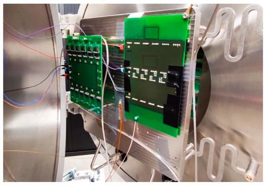
Figure 1.
The sample holder inside the thermal vacuum radiation chamber, which was developed at the National Accelerator Centre (CAN) in Spain.
Overall, five irradiation steps were carried out during the test campaign. During the pristine stage and after each irradiation step, all devices were measured using a Keysight B1505A semiconductor device power analyser to obtain the electrical characteristic metrics. The V-I characteristics were measured at 25 °C after irradiation for 30 min.
Figure 2 shows a block diagram of the test procedure. The static electrical measurements (transfer (Ids-Vgs), gate Schottky diode (Ig-Vgs), drain to source leakage current (Idss-Vds), and gate leakage current (Igss-Vds)) were performed after each exposure step for all devices, including the control devices.
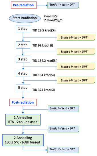
Figure 2.
A schematic diagram of the experimental procedure of the gamma test campaign.
At the end of the total irradiation, two annealing steps were implemented. The first annealing step consisted of room temperature annealing under bias conditions for 24 h. Afterwards, accelerated ageing was carried out, in which the devices were baked at 100 ± 5 °C under bias conditions for 168 h. In both annealing steps, the bias voltage that was applied to each DUT was the same as that applied during the irradiation steps.
During irradiation, the devices were biased under two different conditions with two different controlled temperatures: (1) OFF with voltage stress in the drain and the gate (Vds = 500 V and Vgs = −5 V); (2) OFF with voltage stress in drain (Vds = 500 V and Vgs = 0 V). The devices that were irradiated under these two different bias conditions were also subjected to two different temperatures: half of the devices were irradiated at 53 °C and the other half of the devices were irradiated at 133 °C.
Concerning the measurements, two types were performed: the I–V measurements were conducted using a power device analyser (B1505A) and the RON measurements were conducted using a custom double pulse circuit (Figure 3) [15]. The implemented switching circuit had the benefit of being able to fully control the time that the voltage stress was applied to the GaN HEMT. Basically, it consisted of two transistors that were connected in series between the drain and the source with a resistive load in between.
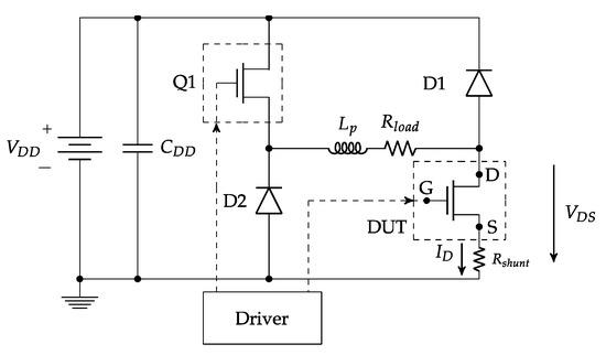
Figure 3.
The circuit diagram that was used to measure the dynamic RON.
Transistor Q1 was used to control the stress/trapping time. A resistive load (Rload) was used to set the current level when the DUT was in the on state. Due to the inherent parasitic inductance (Lp) of the power Rload, two SiC diodes (D1 and D2) offered a freewheeling path for the current when either Q1 or the DUT was switched from on to off. The test sequence of the double pulse measurement is shown in Figure 4. This sequence consisted of stressing the device with a drain voltage for 60 s while it was in the off state and then switching the device to the on state for two pulses of 200 μs, which were separated by an off state of 20 μs. These consecutive pulses that followed the voltage stress provided information about the main trappings, which were the trappings that were induced by the voltage stress and hot electron effects during the switching events [16,17]. For all tests, the drain voltage stress was 500 V, which represented a derating of 80% as it was fixed [18].
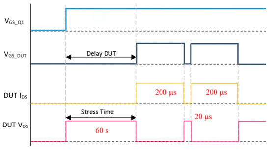
Figure 4.
The gate voltage sequence for the double pulse tests.
For the electrical measurements, we used a 98 mΩ shunt resistor (SDN-414-10) to measure the current and a passive voltage probe (300 V and 500 MHz PP018, Teledyne-Lecroy, CA, USA) to measure the voltage. Owing to the high voltage that was applied to the DUTs, the voltage across the devices had a large dynamic range that could overload the oscilloscope input amplifier, so the on-state voltage could not be determined accurately. To avoid this problem, a voltage clamp circuit was used together with the passive voltage probe. A commercial voltage clamp (clp1500V15A1, Springburo GmbH, Emmendingen, Germany) was used. A low range (2 V) was selected in the voltage clipper to obtain a fast response of 100 ns, which was affected by the passive voltage probe and the voltage clipper. Precise frequency response compensation was applied to the passive voltage probe to compensate for the whole measurement chain of the clipper and voltage probe.
3. Results and Discussion
The effects of gamma radiation on voltage and temperature stress conditions were different. In this section, we analyse the changes in the static and dynamic characteristics by considering the combinations of stress bias conditions and base temperatures that were applied.
3.1. Irradiation at a High Temperature (133 °C)
The devices that were irradiated at 133 °C, regardless of the stress bias voltage conditions, suffered from degradation due to the monotonous increase in drain leakage current (Id), which mostly originated from the increase in gate leakage current (Ig) while the source and substrate currents only offered minor contributions when the total dose was progressively increased. Figure 5 presents the drain leakage current that was measured at 25 °C after each step of irradiation for 30 min using a B1505A semiconductor power parameter analyser. We observed a fourfold increase in the gate current of the G3 device and a sevenfold increase in that of the G4 device, both of which were measured at 600 V.
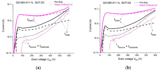
Figure 5.
The leakage currents versus drain voltages in the off state (VGS = 0 V) before (black lines) and after (magenta lines) gamma radiation with a total ionising dose of 374 krad(SiO2) which were stressed during irradiation with VDS = 500 V and VGS = 0 at a base temperature of 133 °C. (a) Device G3 (b) Device G4.
With higher temperatures, the trapping process became faster and the time constants decreased. Additionally, in the off-state condition, when a high drain bias was applied to the device, the drain leakage increased and was favoured by the injection of electrons from the substrate into the GaN layer, which was also strongly dependent on the temperature [19,20].
Figure 6 shows a schematic representation of the trapping processes for two different bias conditions that were used. In the figure, we present the two drain leakage paths that appeared during the GaN HEMT reverse condition tests. In the off state, the trapping processes could occur both at the gate–drain surface (due to the high electric fields between the gate and the drain terminal) and the buffer (due to the large vertical field under the drain).
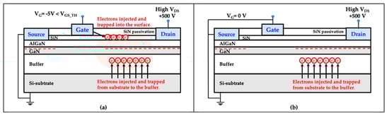
Figure 6.
A schematic representation of the trapping processes in the analysed GaN HEMTs during the two off-state stresses. (a) Whit negative gate voltage. (b) Whit zero gate voltage.
The drain–source current path was established across the silicon substrate and the silicon/nucleation layer interface due to inefficient isolation between the GaN buffer and the Si substrate. It has been reported [21] that the reverse drain leakage of GaN-on-Si HEMTs is due to the injection of electrons into the GaN buffer layer and the tunnelling leakage current of the Schottky gate reverse bias. Therefore, the accumulation of negative charge in the buffer, which is favoured by the positive drain voltage, originates from the increase in dynamic on-resistance (RON). This vertical leakage that fills the buffer traps is interrelated between the trapping rate and the vertical drain–substrate current [22].
During the process of reverse gate bias, the AlGaN/GaN interface trap captured electrons in the channel and caused a negative shift of the threshold voltage. Additionally, the Schottky contact of the gate electrode began to irreversibly degenerate under both the high temperature that was applied during radiation and the high electric field that decreased the height of the Schottky barrier.
Considering the voltage stress that was applied during radiation, it was also observed that when a negative voltage (Vgs = −5 V) was applied to the gate together with a positive drain voltage (sample G2), the increase in the leakage gate current was lower (or even decreased) compared to samples that only had voltage stress in the drain and gates that were shorted to the source terminals (sample G4). Negative gate-to-source voltages induced lateral trappings due to the injection of electrons at the gate–drain surface. This injection of electrons could help to reduce the number of holes that were created by the gamma irradiation and, therefore, helped to reduce the increases in gate leakage current (Figure 7).
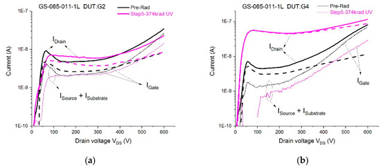
Figure 7.
The leakage currents versus drain voltages in the off state (VGS = 0 V) before (black lines) and after (magenta lines) gamma radiation with a total ionising dose of 374 krad(SiO2) at a base temperature of 133 °C. (a) Device G2 stressed during irradiation with VDS = 500 V and VGS = −5 V. (b) Device G4 stressed during irradiation with VDS = 500 V and VGS = 0.
The dynamic on-resistance is a parameter that is dependent on the trapping or detrapping rate. Thus, we needed to consider the influence of gamma radiation on the trapping processes to establish the relationships between the obtained results and the dynamic on-resistance. The effects of irradiation depend on the structures, temperatures, pre-existing trap densities, dose rates, total accumulated doses, and experimental bias conditions that are applied during irradiation. The improvement or degradation of the electrical characteristics (e.g., gm, ID, RON, Vth) have been discussed in the literature [23,24,25].
When gamma rays are focused on matter, a process of matter ionisation occurs, primarily via indirect ionisation. Electrons interact and may become absorbed, scatter, or produce electron–positron pairs, depending on their energy. Overall, low doses of accumulated radiation result in improvements and when higher doses are applied, degradation begins. In our case, the rate that was achieved was not very high (374 krad) and we distinguished between improvement or degradation depending on the temperature that was applied during the irradiation tests.
In any case, the effects of gamma radiation together with the higher temperature created an increase in the gate leakage current and a shift in the threshold voltage to the left, which caused the degradation of the HEMT and an increase in the dynamic on-resistance, as we explain later.
3.2. Irradiation at a Low Temperature (53 °C)
In the case of irradiation with a lower temperature, regardless of the applied voltage stress, a decrease in the drain current was observed, which was mainly caused by a reduction in the source–substrate current of around 60%. There was no increase in the gate leakage current; however, differences were observed depending on whether the DUT was stressed with VDS = 500 V and VGS = −5 V or VDS = 500 V and VGS = 0. The devices that were stressed during irradiation with VDS = 500 V and VGS = −5 V (G6 and G7) showed a higher reduction (60%) in the drain leakage current than the devices (G8 and G10) that were only stressed with VDS = 500 V (45%). With a negative gate voltage, there was an indicative reduction in the gate leakage current that was additional to the reduction in the source–substrate leakage current, which was due to the compensation of the hole traps by the existence of additional electron traps under the gate that were induced by the negative gate bias during irradiation (Figure 8).
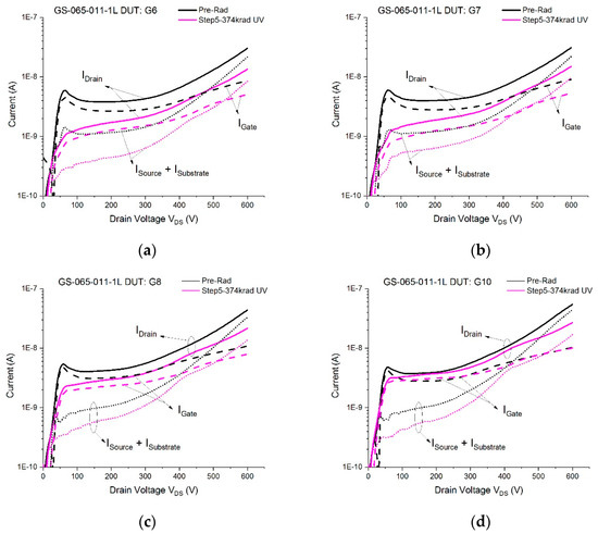
Figure 8.
The leakage currents versus drain voltages in the off state (VGS = 0 V) before (black lines) and after (magenta lines) gamma radiation with a total ionising dose of 374 krad(SiO2) at a base temperature of 53 °C. (a) Device G6 stressed during irradiation with VDS = 500 V and VGS = −5 V. (b) Device G7 stressed during irradiation with VDS = 500 V and VGS = −5 V. (c) Device G8 stressed during irradiation with VDS = 500 V and VGS = 0. (d) Device G10 stressed during irradiation with VDS = 500 V and VGS = 0.
In off-state conditions, trapping could occur both at the gate–drain surface and the buffer. The increase in RON mainly originated from buffer traps. This process could be explained by two different mechanisms: an electrostatic effect of the high negative gate–drain voltage that depleted the hole traps in the buffer and the flow of vertical drain current.
Our results, in concordance with previous investigations [25], showed an improvement in the electrical properties of the devices due to the decrease in leakage current when gamma irradiation was applied. This reduction could be attributed to the reduction in the density of traps, along with the ordering of native defects, but it needs to be verified by scanning transmission electron microscopy (STEM) to characterise the defects and elemental distributions. The reduction in the drain–substrate leakage helped to reduce on-state trapping in the device and, therefore, the dynamic RON.
3.3. Dynamic RON
The results of the dynamic on-resistance tests are shown in Figure 9. After a stress of VDS = 500 V was applied to the GaN HEMTs in the off state, two pulses were applied (Figure 4) using a double pulse test (DPT) circuit to measure the dynamic on-resistance.
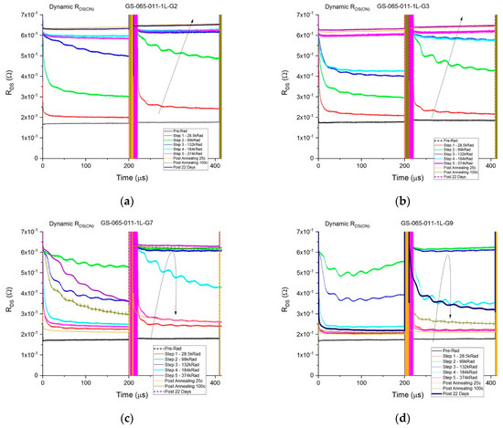
Figure 9.
The dynamic RON double pulse measurements in the off state (VDS = 500 V and VGS = −5 V) and on state (VGS = 3 V and IDS = 2.5 A): (a) device G2, which was subjected to drain and gate voltage stress during irradiation at 133 °C; (b) device G3, which was subjected to drain voltage stress during irradiation at 133 °C; (c) device G7, which was subjected to drain and gate voltage stress during irradiation at 53 °C; (d) device G9, which was subjected to drain voltage stress during irradiation at 53 °C.
In all of the devices that were subjected to gamma radiation at the higher temperature (133 °C), regardless of the voltage stress that was applied (Table 1), a degradation of the dynamic RON was observed, which increased with the total ionising dose and was not recoverable after the two-step annealing process (Figure 9a,b). For the devices that were irradiated at the lower temperature (53 °C), the dynamic on-resistance increased with the accumulated dose until it reached step 4 (184 krad(SiO2)) when the RON started to reduce in value and it only increased after the 100 °C annealing process, which was permanent (Figure 9c,d).
In Figure 9, increases in dynamic RON can be observed that were higher in the second pulse than in the first. This was evidence of a trapping process, which was induced by hot electrons during the semi-on state of the switching events. Under hard-switching conditions, the GaN HEMTs were simultaneously subjected to high drain voltages and a rising drain current. The electrons that were injected from the source to the drain were accelerated by the high electric field (usually called “hot electrons”).
In order to quantify the evolution of dynamic RON during the irradiation process, we measured the average value of RON during an interval of 20 μs at the end of the second pulse. Figure 10 shows the evolution of the dynamic RON values for all of the devices during all of the radiation steps throughout the test campaign.
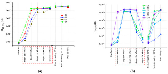
Figure 10.
The RON double pulse measurements: (a) devices G1–G4, which were irradiated at 133 °C; (b) devices G5–G10, which were irradiated at 53 °C.
All of the devices that were irradiated at 133 °C suffered from an increase in RON that reached saturation at 99 krad(SiO2) or 132 krad(SiO2), which was indicative of the saturation of the electric charge traps in the devices that, in turn, limited the total ionising dose (TID) effects. However, in the devices that were irradiated at the lower temperature (53 °C), the resistance increased with the total accumulated dose and become saturated close to 99 krad(SiO2) and began to decrease in the range of 132–184 krad(SiO2). Finally, in the annealing step at 100 °C, a permanent degradation was observed.
It was also mandatory to investigate the behaviour of dynamic RON when multiple pulses were applied. The multi-pulse test (MPT) was conducted using the circuit setup that was shown in Figure 3, but with a driving signal test sequence of multiple pulses, a stress time of 500 ms, and an on-time of 6 us. The multi-pulse sequence finished once the stationary value of RON was found, using a mathematical function in the digital oscilloscope that was used to record the drain current and drain voltage waveforms [15]. The results are shown in Figure 11 and Figure 12.
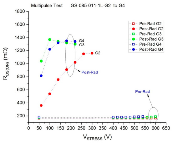
Figure 11.
The results of the multi-pulse test for the RON values of devices G2–G4, which were irradiated at 133 °C.
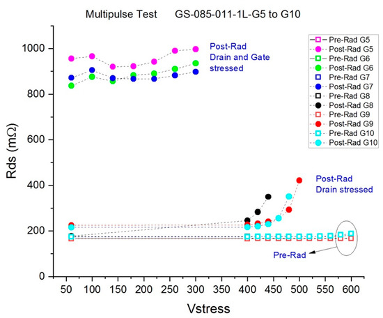
Figure 12.
The results of the multi-pulse test for the RON values of devices G5–G10, which were irradiated at 53 °C.
Figure 11 confirms the irreversible increase in RON when the temperature during irradiation was 133 °C, regardless of the stress that was applied to the drain and/or gate.
Similarly, Figure 12 shows the influence of the negative voltage stress that was applied to the gate during irradiation. Despite being irradiated at a lower temperature (53 °C), the devices with stress at the drain and gate (VDS = 500 V and VGS = −5 V) demonstrated degradations in dynamic RON once the radiation accumulated. The RON value was five times higher, regardless of the applied stress voltage. It could be seen that, for VDS = 500 V in the off state, the RON reached its maximum value and did not change when a higher stress voltage was applied.
In the devices to which voltage stress was applied to the drain and in which the gate was short-circuited with the source, the RON remained practically constant between 50 and 400 V of applied stress, and it started to increase almost exponentially from 500 V.
4. Conclusions
In this work, we investigated the impacts of gamma radiation on commercial off-the-shelf Schottky-type p-gate AlGaN/GaN HEMTs by considering temperature and voltage bias stress as influence variables. The acceleration of the trapping kinetics (due to the higher temperature) and the injection of electrons from the substrate into the trap sites (due to the high off-state voltage stress) caused an increase in RON that could seriously undermine the device’s performance.
This trapping rate was higher than the accumulation rate of positive charges (holes or ionised donors). These positive charges, which resulted from electron–hole pairs that were created by radiation-induced ionisation, had lower mobilities at higher temperatures and, thus, did not allow the holes to migrate or recombine, thereby reducing the radiation impacts.
However, at lower temperatures, the trapping effects were less and as the rate of accumulated radiation increased, there was a partial recovery in dynamic RON that could be attributed to dispersion effects from the buffer traps, according to different explanations from the literature: trapped holes in C-related traps partially neutralise negative ionised acceptors [26]; the neutralisation of negative and positive buffer charge storage [27], which is induced by leakage paths between 2D electron gas (2DEG) and C-doped buffer; the generation of positive charges via the ionisation of donor traps in the unintentionally doped (UID) GaN channel layer [28].
From the point of view of the design of power converters for space applications, where silicon MOSFET technology is to be replaced by GaN HEMTs, reliability is an essential requirement due to the harsh environments. The multi-pulse test confirmed that RON could permanently degrade five times faster (for an accumulated dose of 374 krad(SiO2)), depending on the temperature and the voltage stress that was applied during the off interval. The most favourable conditions were when the temperature of the device during irradiation was in the order of 60 °C (in accordance with the standard base temperature of power stages in satellites) and negative voltage stress was not applied to the gate of the device and the only stress was the voltage in the drain and the semi-on conditions during the switching operation. In that case, the degradation was lower and did not appear until a voltage stress of around 450 V was applied.
The impact of gamma radiation on the RDS(ON) performance of the device is an important issue due to an increase in this value will have a very significant impact on the power converter losses, especially in hard-switching mode, where the overlap between voltage and current favours the trapping effect. In addition, this increase in power losses will cause an increase in temperature and the effects of charge trapping can be favoured by this increase in temperature. This effect and temperature dependency lead to a difficult thermal design of the converter. Additionally, the increase in temperature can degrade the forward Schottky characteristic of the gate resulting in a positive shift of the gate to the source voltage threshold, affecting the driving requirements of the driver circuit.
Therefore, it would be necessary to control the temperature of GaN HEMTs in radiation environments in addition to the drain–source blocking voltage so that they can withstand the conditions during the off intervals and the passivation phases of satellites.
Author Contributions
E.M. conceived the idea, designed the experiment, guided the experiment, and wrote the manuscript; P.M.-H. conducted most of the device measurements and controlled the radiation step, Y.M. radiation supervision of the device measurements and controlled radiation steps; D.G. and E.S.-K. helped with the data analysis and the setup design. P.J.M. contributed to the results analysis and the discussion of the conclusions. All authors have read and agreed to the published version of the manuscript.
Funding
This work was partially supported by the Spanish Ministry of Science, Innovation and Universities and the European Regional Development Fund (ERDF) under grant number RTI2018-099009-B-C22.
Institutional Review Board Statement
Not aplicable.
Informed Consent Statement
Not aplicable.
Data Availability Statement
The data presented in this study are available on request from the corresponding autor.
Conflicts of Interest
The authors declare no conflict of interest.
References
- Jones, E.A.; Wang, F.F.; Costinett, D. Review of commercial GaN power devices and GaN-based converter design challenges. IEEE J. Emerg. Sel. Top. Power Electron. 2016, 4, 707–719. [Google Scholar] [CrossRef]
- Teo, K.H.; Zhang, Y.; Chowdhury, N.; Rakheja, S.; Ma, R.; Xie, Q.; Yagyu, E.; Yamanaka, K.; Li, K.; Palacios, T. Emerging GaN technologies for power, RF, digital, and quantum computing applications: Recent advances and prospects. J. Appl. Phys. 2021, 130, 160902. [Google Scholar] [CrossRef]
- Dalla Vecchia, M.; Ravyts, S.; Van den Broeck, G.; Driesen, J. Gallium-Nitride Semiconductor Technology, and Its Practical Design Challenges in Power Electronics Applications: An Overview. Energies 2019, 12, 2663. [Google Scholar] [CrossRef]
- Son, K.A.; Liao, A.; Lung, G.; Gallegos, M.; Hatake, T.; Harris, R.D.; Scheick, L.Z.; Smythe, W.D. GaN-Based High Temperature and Radiation-Hard Electronics for Harsh Environments. Nanosci. Nanotechnol. Lett. 2010, 2, 89–95. [Google Scholar] [CrossRef]
- Notarianni, M.; Messant, B.; Maynadier, P. Using GaN HFET to replace MOSFET in DC/DC for space applications. In Proceedings of the 2019 European Space Power Conference (ESPC), Juan Les Pins, France, 30 September–4 October 2019; pp. 1–3. [Google Scholar] [CrossRef]
- Wenping, G.; Chi, C.; Huantao, D.; Yue, H.; Jincheng, Z.; Chong, W.; Qian, F.; Xiaohua, M. 60Co γ-rays irradiation effect in DC performance of AlGaN/GaN high electron mobility transistors. J. Semicond. 2009, 30, 044002. [Google Scholar] [CrossRef]
- Vitusevich, S.A.; Klein, N.; Belyaev, A.E.; Danylyuk, S.V.; Petrychuk, M.V.; Konakova, R.V.; Kurakin, A.M.; Rengevich, A.E.; Avksentyev, A.Y.; Danilchenko, B.A.; et al. Effects of γ-irradiation on AlGaN/GaN-based HEMTs. Phys. Stat. Sol. 2003, 195, 101–105. [Google Scholar] [CrossRef]
- Sun, X.; Saadat, O.I.; Chen, J.; Zhang, E.X.; Cui, S.; Palacios, T.; Fleetwood, D.M.; Ma, T.P. Total-ionizing-dose radiation effects in AlGaN/GaN HEMTs and MOS-HEMTs. IEEE Trans. Nucl. Sci. 2013, 60, 4074–4079. [Google Scholar] [CrossRef]
- Chang, S.J.; Kim, D.S.; Kim, T.W.; Lee, J.H.; Bae, Y.; Jung, H.W.; Kang, S.C.; Kim, H.; Noh, Y.S.; Lee, S.H.; et al. Comprehensive research of total ionizing dose effects in GaN-based MIS-HEMTs using extremely thin gate dielectric layer. Nanomaterials 2020, 10, 2175. [Google Scholar] [CrossRef]
- Yang, C.Y.; Chung, C.H.; Yu, W.; Ma, C.J.; Wu, S.R.; Dixit, A. A Comprehensive Study of Total Ionizing Dose Effect on the Electrical Performance of the GaN MIS-HEMT. IEEE Trans. Device Mater. Reliab. 2022, 22, 276–281. [Google Scholar] [CrossRef]
- Chen, S.Y.; Yu, X.; Lu, W.; Yao, S.; Li, X.L.; Wang, X. Effects of Total-Ionizing-Dose Irradiation on Single-Event Burnout for Commercial Enhancement-Mode AlGaN/GaN High-Electron Mobility Transistors. Chin. Phys. Lett. 2020, 37, 4. [Google Scholar] [CrossRef]
- GaN System. “GS-065-011-1-L“ Rev 220708, July 2022. Available online: https://gansystems.com/wp-content/uploads/2022/07/GS-065-011-1-L-DS-Rev-220708.pdf (accessed on 9 October 2022).
- European Space Agency. Total Dose Steady-State Irradiation Test Method; ESCC Basic Specification No. 22900; European Space Agency: Paris, France, 2016. [Google Scholar]
- Martín-Holgado, P.; Romero, Á.J.; Labrador, J.A.; Vizcaíno, A.; Herranz, J.; Morilla, Y. First Chamber in Spain to Irradiate at Low and High Temperature with Gamma, Neutrons and Low-Energy Protons. In Proceedings of the 2020 20th European Conference on Radiation and Its Effects on Components and Systems (RADECS), Toulouse, France, 19 October–20 November 2020; pp. 1–5. [Google Scholar] [CrossRef]
- Martínez, P.J.; Maset, E.; Martín-Holgado, P.; Morilla, Y.; Gilabert, D.; Sanchis-Kilders, E. Impact of Gamma Radiation on Dynamic RDSON Characteristics in AlGaN/GaN Power HEMTs. Materials 2019, 12, 2760. [Google Scholar] [CrossRef] [PubMed]
- Meneghesso, G.; Meneghini, M.; Bisi, D.; Rossetto, I.; Cester, A.; Mishra, U.K.; Zanoni, E. Trapping phenomena in AlGaN/GaN HEMTs: A study based on pulsed and transient measurements. Semicond. Sci. Technol. 2013, 28, 074021. [Google Scholar] [CrossRef]
- Rossetto, I.; Meneghini, M.; Tajalli, A.; Dalcanale, S.; De Santi, C.; Moens, P.; Banerjee, A.; Zanoni, E.; Meneghesso, G. Evidence of Hot-Electron Effects during Hard Switching of AlGaN/GaN HEMTs. IEEE Trans. Electron Devices 2017, 64, 3734–3739. [Google Scholar] [CrossRef]
- Drabbe, J. Space Product Assurance: Derating—EEE Components; ECSS-Q-ST-30-11C Rev 1; Requirements & Standards Division: Noordwijk, The Netherlands, 2011. [Google Scholar]
- Meneghini, M.; Silvestri, R.; Dalcanale, S.; Bisi, D.; Zanoni, E.; Meneghesso, G. Evidence for temperature-dependent buffer-induced trapping in GaN-on-silicon power transistors. In Proceedings of the 2015 IEEE International Reliability Physics Symposium, Monterey, CA, USA, 23–29 April 2015; pp. 2E.2.1–2E.2.6. [Google Scholar] [CrossRef]
- Meneghini, M.; Vanmeerbeek, P.; Silvestri, R.; Dalcanale, S.; Banerjee, A.; Bisi, D.; Zanoni, E.; Meneghesso, G.; Moens, P. Temperature-Dependent Dynamic Ron in GaN-Based MIS-HEMTs: Role of Surface Traps and Buffer Leakage. Electron. Devices IEEE Trans. 2015, 62, 782–787. [Google Scholar] [CrossRef]
- Bahat-Treidel, E.; Brunner, F.; Hilt, O.; Cho, E.; Wurfl, J.; Trankle, G. Electron Devices. IEEE Trans. 2010, 57, 3050. [Google Scholar] [CrossRef]
- Pérez-Tomás, A.; Fontserè, A.; Llobet, J.; Placidi, M.; Rennesson, S.; Baron, N.; Chenot, S.; Moreno, J.C.; Cordier, Y. Analysis of the AlGaN/GaN vertical bulk current on Si, sapphire, and free-standing GaN substrates. J. Appl. Phys. 2013, 113, 174501. [Google Scholar] [CrossRef]
- Sharma, C.; Modolo, N.; Wu, T.L.; Meneghini, M.; Meneghesso, G.; Zanoni, E. Understanding γ Ray Induced Instability in AlGaN/GaN HEMTs Using a Physics-Based Compact Model. IEEE Trans. Electron Devices 2020, 67, 1126–1131. [Google Scholar] [CrossRef]
- Hwang, Y.H.; Hsieh, Y.L.; Lei, L.; Li, S.; Ren, F. Effect of low dose gamma-irradiation on DC performance of circular AlGaN/GaN high electron mobility transistors. J. Vac. Sci. Technol. B 2014, 32, 205–210. [Google Scholar] [CrossRef]
- Pan, S.; Feng, S.; Li, X.; Zheng, X.; Lu, X.; Hu, C.; Hu, X.; Bai, K.; Zhou, L.; Zhang, Y. Effects of gamma irradiation on GaN high-electron-mobility transistors characterized by the voltage-transient method. Semicond. Sci. Technol. 2021, 36, 095011. [Google Scholar] [CrossRef]
- Cioni, M.; Zagni, N.; Iucolano, F.; Moschetti, M.; Verzellesi, G.; Chini, A. Partial Recovery of Dynamic RON Versus OFF-State Stress Voltage in p-GaN Gate AlGaN/GaN Power HEMTs. IEEE Trans. Electron Devices 2021, 68, 4862–4868. [Google Scholar] [CrossRef]
- Moens, P.; Uren, M.J.; Banerjee, A.; Meneghini, M.; Padmanabhan, B.; Jeon, W.; Karboyan, S.; Kuball, M.; Meneghesso, G.; Zanoni, E.; et al. Negative dynamic Ron in AlGaN/GaN power devices. In Proceedings of the 2017 29th International Symposium on Power Semiconductor Devices and IC’s (ISPSD), Sapporo, Japan, 28 May–1 June 2017; pp. 97–100. [Google Scholar] [CrossRef]
- Yang, S.; Han, S.; Sheng, K.; Chen, K.J. Dynamic on-resistance in GaN power devices: Mechanisms characterizations and modeling. IEEE J. Emerg. Sel. Topics Power Electron. 2019, 7, 1425–1439. [Google Scholar] [CrossRef]
Publisher’s Note: MDPI stays neutral with regard to jurisdictional claims in published maps and institutional affiliations. |
© 2022 by the authors. Licensee MDPI, Basel, Switzerland. This article is an open access article distributed under the terms and conditions of the Creative Commons Attribution (CC BY) license (https://creativecommons.org/licenses/by/4.0/).