Article

Dirac-Based Quantum Admittance of 2D Nanomaterials at Radio Frequencies

Department of Information Engineering, Università Politecnica delle Marche, 60131 Ancona, Italy
*
Author to whom correspondence should be addressed.
Appl. Sci. 2022, 12(24), 12539; https://doi.org/10.3390/app122412539
Submission received: 18 November 2022 / Revised: 4 December 2022 / Accepted: 5 December 2022 / Published: 7 December 2022
(This article belongs to the Section Applied Physics General)

Abstract

:
Starting from a rigorous finite mass, Dirac equation-based model, we investigate the R.F. quantum admittance of a monolayer 2D material under the action of an electromagnetic (e.m.) wave with axially directed vector potential. With some reasonable approximations, the analysis yields a relatively simple RLC-equivalent circuit with frequency-independent elements depending on the bias, temperature, effective mass, Fermi velocity and effective e.m. index of the material, losses and other relevant parameters.

1. Introduction

The drive toward circuit miniaturization and the advent of new materials, such as graphene, has led to a situation where the quantum current flows on mesoscopic and nanoscopic conductors. The quantum current and conductivity in nanostructures present novel and interesting aspects that have been the subject of much interest in recent years. In evaluating this kind of situation with a finite electron mass, the Schrödinger equation from quantum mechanics has been used in the framework of a free electron model, where electrons are described by scalar wave functions. This description is, however, incomplete when the polarization and magnetization aspects become important (e.g., in the common situation of applied electromagnetic fields). In such a case, the use of a four-component Dirac spinor description becomes necessary. In a conductor in particular, the scalar ratio between the first pair of components and the second pair plays the role of characteristic impedance of a transmission line, where the ratio of source impedance to load impedance is essential for the correct definition of transmittivity. In a previous work [1], we derived from the Dirac equation with a finite effective mass the quantum current in the presence of a d.c. electric field parallel to the surface of a 2D nanomaterial and, consequently, the d.c. conductivity. In the literature, a large number of works address the problem of charge transport in low-dimensional structures and related applications [2,3,4,5,6,7,8,9,10,11,12,13,14,15,16,17,18,19,20,21,22,23,24,25]. In this work, we consider the action of an R.F. electric field in the same idealized 2D geometry. In the case of a device with dimensions much smaller than the electromagnetic wavelength, the electromagnetic boundary conditions of the field can be neglected, and the tensor character of the admittance can be approximated as scalar since the cross-impedance effect is low. Real loss mechanisms, such as intra-band transitions and interaction with the substrate, are subsumed by a global, finite mean free path L F . Our aim is to extend the calculation of the scalar quantum conductivity previously performed in the d.c. case to the case of the R.F. admittance. The amplitude of the driving R.F. field is assumed initially to not be depleted by losses and be unaffected by the current on the surface (low loss approach). Once the current has been evaluated, losses are introduced in the potential, leading to the complex R.F. admittance at the signal frequency. The intensity of the R.F. signal is assumed to be moderate enough to not affect the electron density or Fermi distribution, and its action is assumed to start at x = 0 and t = 0.

2. Dirac Equation

Considering the problem in Figure 1, the Dirac equation in x and t, with a finite effective mass m e and Fermi velocity v F in the band of interest, is
v F α x i x + | e | A + β m e v F 2 Ψ = i t + | e | Φ Ψ
where | e | Φ stands for the energy related to the total scalar potential Φ , which is due to the d.c. electric field as well as that associated with the vector potential A. When dealing with the modulation of a time harmonic, namely a very high frequency carrier (e.g., optical) by a radio frequency (R.F.), it is expedient to separate the large but constant contribution of the carrier frequency ω c from that of the time modulation by writing
t = i ω c + τ .
In the present case, the “rest” energy is
m e v F 2 = 2 E F
where in the case of parabolic dispersion, in absence of doping and identifying m e with the cyclotron mass, it is usually much larger than all other contributions.It is therefore appropriate to extract from the Hamiltonian on the RHS of Equation (1) its stationary terms by rewriting it as
i t = m e v F 2 + E + i τ
where τ is the time scale of the modulation and E is the stationary state energy we are considering. Clearly, we have to integrate over the range of possible E’ values. Schrödinger’s equation is actually recovered from Equation (1) by repeated application of the Hamiltonian operator in the limit m e v F 2 E , neglecting the squares of the potentials and passing from a spinor to a scalar wave function by equating the currents. Moreover, we have in Equation (1) that
V = V 0 + E 0 x
Φ = V + ϕ x , τ
where V 0 is the d.c. bias constant in space and time, E 0 is the constant d.c. field, if any, and ϕ is the time-dependent scalar potential associated with the vector potential A such that the Lorentz gauge is satisfied:
· A + 1 v 2 τ ϕ = 0
In our case, by disregarding transverse variation over the ribbon width ( 2 π / k L y , where k is the wavenumber in the media) and boundary conditions of the e.m. field, we assume an x-directed vector potential
A = A ^ e i k x x ω τ x ^
that implies a scalar potential ϕ = v 2 / ω k x A ^ e i ( k x x ω τ ) = n e v A , where n e = k x / k 0 is the “effective” “index” of the propagating wave. The Dirac equation (Equation (1)) is now cast in the working form
α x x + i | e | A i | e | ϕ v F + 1 v F τ Ψ = i v F E + E v + m e v F 2 I m e v F 2 β Ψ
where I is the 4 × 4 identity matrix and E v = | e | V is the d.c. field energy. As mentioned, we also subsume constant small losses (e.g., due to interaction with the substrate) over a finite mean free path L F , leading to a propagation decay of the type e x / L F , simply by replacing x with x ± 1 / L F according to whether the wave is progressive or regressive. This modification keeps the remainder of the equation Hermitian in nature. The solution of the system of the partial differential equation (Equation (9)) is uniquely determined by the initial and boundary conditions. A proper definition of quantum admittance also requires no return wave and a proper input match at the origin of the computational domain ( 0 x L x ) for a progressive wave traveling from left to right.

3. Spinor Solution

As a preliminary, E V is assumed to be constant either in absence of the d.c. field or following a stepwise approximation of V for modest fields. This expedience allows us to eliminate the inconvenient, constant diagonal matrix on the RHS of Equation (9) by means of a similarity transformation:
Ψ E + E V I 0 0 E + E V + 2 m e v F 2 I Ψ
This reduces to the form of a standard eigenvalue equation:
α x x + i | e | A i | e | ϕ v F + 1 v F τ Ψ = i λ Ψ
where λ 1 / ( v F ) ( E + E V ) ( E + E V + 2 m e v F 2 ) m 1 . The Dirac matrix α x is now the only one appearing in Equation (11). The progressive and regressive traveling wave solutions of Ψ are eigenvectors pertaining to the eigenvalues ± 1. In [1], in fact, it is shown that the spinor Ψ is in the following form:
Ψ = a + b σ x ( a b )
where
a = a 0 a 1 b = b 0 b 1
Setting b = 0 in Equation (12) above retains just the progressive wave, as is required in this case. In the absence of y variation, moreover, we may set a 0 = a 1 = a / 2 .
Since we are now dealing with just one eigenvector, in Equation (11), we may replace the matrix α x with its eigenvalue +1 and reduce Equation (11) to an ordinary differential equation for the scalar a:
x + i | e | ω A ^ ω v 2 v F k x e i ( k x x ω τ ) + 1 v F τ a = i λ 1 L F a
It is expedient to introduce the “angular frequency”
ω 1 v F | e | A ^ ω v 2 k x v F ω v F k x
and the position
a ˜ e x p ω 1 / ω e i ( k x x ω τ ) a
This reduces Equation (14) to the standard transmission line equation
x + 1 v F τ a ˜ = i λ 1 L F a ˜
The progressive wave solution of Equation (17) is
a ˜ ( x , τ ) = e x p x L F + i λ ( x v F τ ) a ˜ ( 0 , 0 )
with a ˜ ( 0 , 0 ) = e x p ( ω 1 / ω ) a ( 0 , 0 ) . Finally, by introducing Equation (18) into Equation (16), we obtain the solution to Equation (14) as follows:
a ( x , τ ; E ) = e x p x L F + i λ ( x v F τ ) + ω 1 ω e i ( k x x ω τ ) 1 a ( 0 , 0 ; E )
In addition, the original spinor Ψ is recovered by means of the inverse transformation of Equation (12):
Ψ = I E + E V 0 0 I E + E V + 2 m e v F 2 Ψ = a 2 1 E + E V 1 E + E V 1 E + E V + 2 m e + v F 2 1 E + E V + 2 m e + v F 2
Equation (19) shows that the R.F. produces frequency modulation as well as a time-retarded traveling wave in the phase of the spinor.

4. Definition of Current
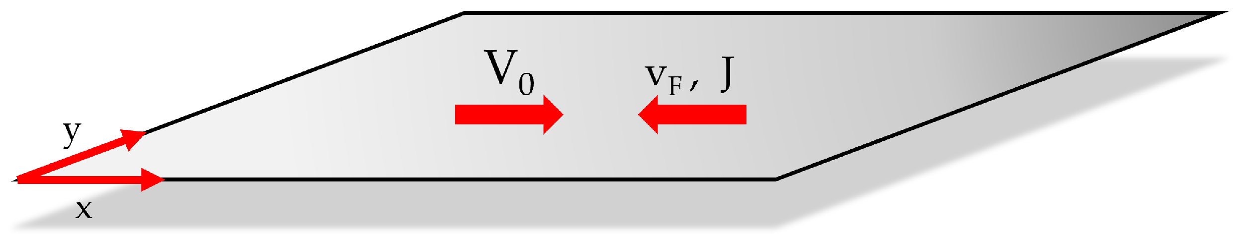
From knowledge of the Dirac spinor Ψ , the general current density vector J ( x , t ; E ) is defined as
J = v F | e | N ( E ) Ψ α Ψ
N ( E ) above is the electron density at the energy E , which is considered to be unaffected by the presence of the R.F. as is reasonable for moderate fields, as reported in [4]. Using Equation (18), the longitudinal component J x is given by
J x = | e | N v F Ψ 0 σ x σ x 0 Ψ = 2 | e | N v F | a | 2 ( E + E V ) ( E + E V + 2 m e v F 2 ) 1
However, Equation (19) gives
| a | 2 = e x p 2 x L F + 2 ω 1 ω c o s ( k x x ω t ) 1 ) | a ( 0 , 0 ; E ) | 2
Adopting the same current normalization as in [1], where J ( 0 , 0 ; E ) = | e | N ( E ) v F , implies that | a ( 0 , 0 ; E ) | 2 = 1 2 ( E + E V ) ( E + E V + 2 m e v F 2 ) and consequently
J x ( x , t ; E ) = | e | N ( E ) v F e x p 2 x L F + 2 ω 1 ω c o s ( k x x ω t ) 1 )
The first term in Equation (24) represents just d.c. losses in the absence of the R.F. signal. As a function of the frequency, the current shows high-pass characteristics. Moreover, there appear to be infinite harmonics of the argument θ = k x x ω t , which is a feature of RF mixers. This fact is made explicit by the identity [2]
e x p 2 ω 1 ω c o s θ = k I k 2 ω 1 ω e i k θ ( k = 0 , ± 1 , ± 2 , )
where I k ( z ) = i k J k ( i z ) are the Bessel functions. Retaining only the fundamental harmonic of the signal (k = 1) yields the scalar admittance at the signal frequency.
We consider now a ballistic regime with flow in the x direction and which is uniform in the y direction. For a band of energies, the electron density N ( E ) is to be replaced by a density of states, weighted by the occupation probability and integrated from the thermodynamic energy limit K B T 25 meV at 300 up to the chemical potential μ . By retaining just the fundamental harmonic in Equation (24), this leads to a current density of
J = 2 | e | v F 1 L x L y e x p 2 x L F + i θ I 1 2 ω 1 ω e 2 ω 1 / ω K B T μ D ( E ) f ( E ) d E [ A m 1 ]
The pre-factor 2, now appearing in Equation (26), is due to two electrons of opposite spins finding places in a state. Moreover, the density of the states is D ( E ) = d N S d k d k d E . Since we are considering a ribbon configuration, we assume the density of the states of a two-dimensional system with parabolic E-k characteristics first. The particular case of graphene will be considered presently.
Apearring in Equation (16) as well, N S = ( π k 2 ) / ( ( 2 π ) 2 L x L y ) is the number of states in the k-space and E = ( k ) 2 / ( 2 m e ) such that:
D ( E ) = d N S d k d k d E = k 2 π L x L y m e 2 k = L x L y m e 2 π 2 = c o n s t .
The probability of occupation, in the presence of the applied voltage V, is
f = 1 1 + e x p ( E ( μ μ 0 ) ) / ( K B T )
where μ μ 0 = E V . Consistent with previous assumptions, we disregard the effect of the R.F. field energy on the probability distribution. The energy integral of Equation (26) is
J = | e | v F m e π 2 e x p 2 x L F + i θ I 1 2 ω 1 ω e 2 ω 1 / ω Δ [ A m 1 ]
where, from the tables in [2] (p. 92), we have
Δ = K B T μ f ( E ) d E = μ K B T 1 l n 1 + e ( K B T ( μ μ 0 ) ) / ( K B T ) ) 1 + e E V / K B T

4.1. Graphene

Graphene provides an important particular case, since the dispersion relation is assumed to be of the type
E ( k ) = ( k ) m e v F 2 m e = v F k 2
This implies a density of states
D ( E ) = 2 E π ( v F ) 2 L x L y [ J 1 ] .
In this case, Equation (29) is replaced by
J = 4 | e | π 2 v F e x p 2 x L F + i θ I 1 2 ω 1 ω e 2 ω 1 / ω Δ [ A m 1 ]
where
Δ K B T μ E f ( E ) d E

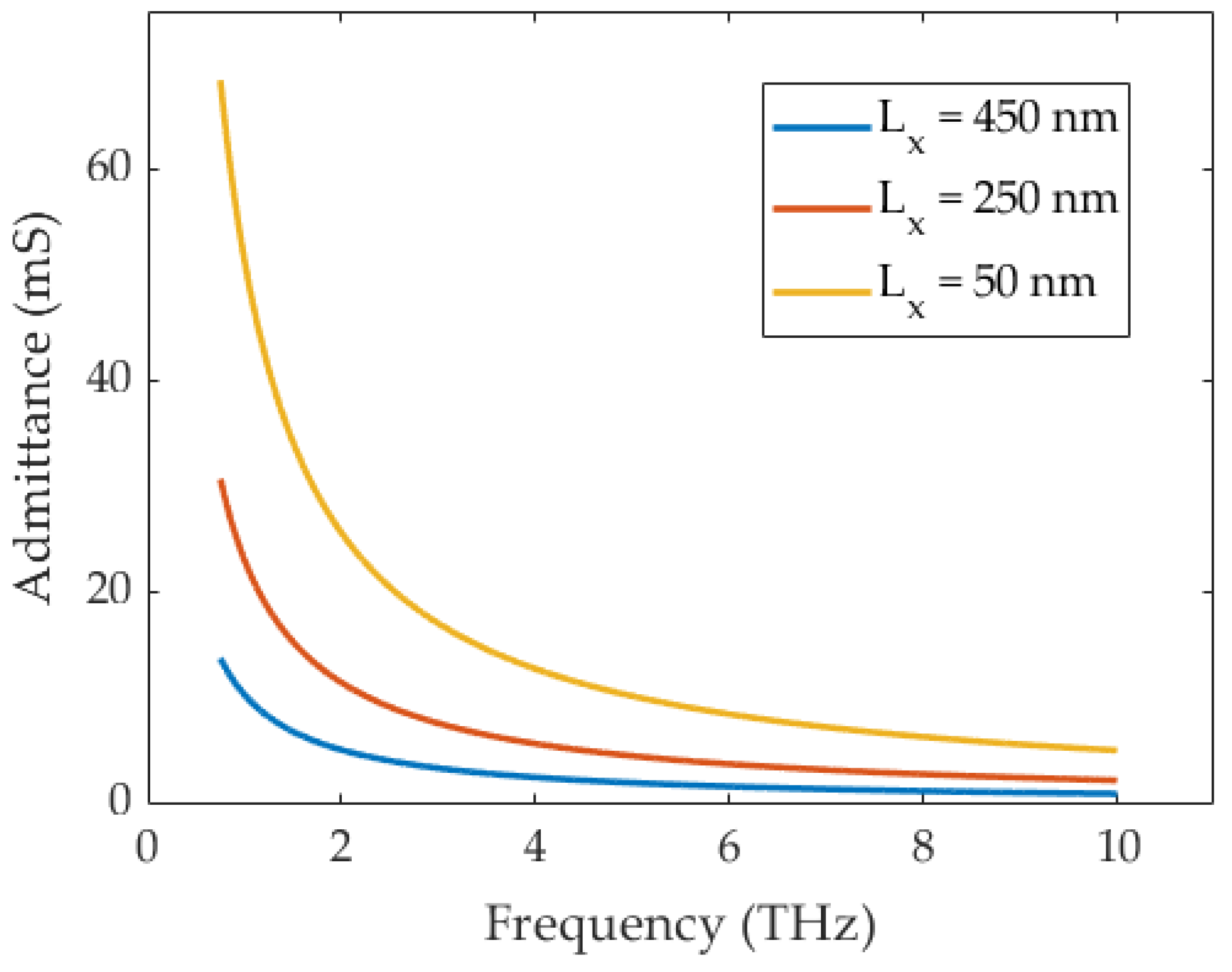
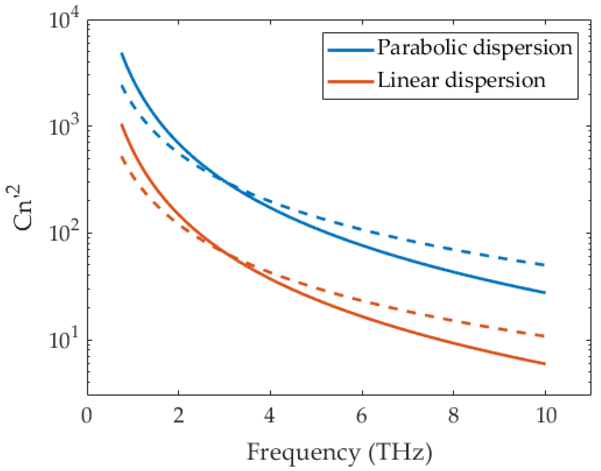
4.2. R.F. Quantum Admittance

The definition of admittance of the main harmonic is
Y ( ω ) = J E [ Ω 1 ]
In our case, E = E x = A / t ϕ / x , ϕ = v 2 k x A / ω is the scalar R.F. potential. The current propagation losses are now introduced in the potential. We have ϕ / x = ( 2 / L F + i k x ) ϕ and
E = i ω A 2 L F + i k x ϕ = 1 i ω v 2 k x 2 ω 2 + i 2 v 2 k x L F A = = 1 i ω v 2 k x 2 ω 2 + i ω 2 v L F n e n A
In the last step, we used the fact that v k x = n e / n ω , where n e is the effective refractive index k x / k 0 of the e.m. wave at the frequency in question and n = c / v . From Equations (26) and (29), at x = L x , we find the following for the parabolic E-k dispersion:
Y ( ω ) = i ω | e | v F m e Δ π 2 e 2 L x / L F 1 A ^ I 1 2 ω 1 ω e 2 ω 1 / ω v 2 k x 2 ω 2 + i ω 2 v L F n e n 1
whereas for the linear dispersion (graphene), we found the following (Equation (38)):
Y ( ω ) = i ω | e | Δ π 2 v F e 2 L x / L F 1 A ^ I 1 2 ω 1 ω e 2 ω 1 / ω v 2 k x 2 ω 2 + i ω 2 v L F n e n 1
Recalling that ω 1 is defined as in Equation(15), we find the following in the limit of the small argument:
Y ( ω ) = i | e | 2 Δ π 3 e 2 L x / L F ω v 2 k x / v F ω v F k x v 2 k x 2 ω 2 + i ω 2 v L F n e n 1
If n e = n , then v k x = ω , and thus:
Y ( ω ) = | e | 2 Δ π 3 e 2 L x / L F L F 2 ω v F
Figure 2 shows the admittance Y in the linear dispersion case in Equation (40) as functions of the frequency for different values of L x , considering the parameters in Table 1. As is shown, as L x approaches to the mean free path, the admittance decreases due to a transition between the ballistic and diffusive transport regimes.
The admittance of Equations (37) or (38) above is the admittance of a series RLC circuit seen through a frequency-dependent ideal transformer n ( ω ) :
Y ( ω ) = j ω C n 2 ω 1 ω 2 L C + j ω R C
where j = i , L C = 1 / ( v 2 k x 2 ) , R C = ( 2 v / L F ) ( n e / n ) ( 1 / ( v 2 k x 2 ) ) and
C n 2 ( ω ) = | e | v F m e Δ π 2 v 2 k x 2 e 2 L x / L F 1 A ^ I 1 2 ω 1 ω e 2 ω 1 / ω
C n 2 ( ω ) = | e | Δ π 2 v 2 k x 2 v F e 2 L x / L F 1 A ^ I 1 2 ω 1 ω e 2 ω 1 / ω
for the parabolic and linear dispersion cases, respectively.
In the small argument limit (weak field and high frequency), we have I 1 ( z ) e z z / 2 , whereas for large arguments (high field and low frequency), we have I 1 ( z ) e z 1 / 2 π z . In the former limit, recalling that ω 1 is defined as in Equation (15), we obtain
C n 2 ( ω ) = | e | 2 v F 2 m e Δ π 2 v 2 k x 2 e 2 L x / L F 1 ω ω ( v 2 k x ) / v F ω v F k x
C n 2 ( ω ) = | e | 2 v F Δ π 2 v 2 k x 2 v F e 2 L x / L F 1 ω ω ( v 2 k x ) / v F ω v F k x
for the parabolic and linear dispersion cases, respectively.
In the high field and low frequency limit, we obtain
C n 2 ( ω ) = | e | v F m e Δ π 2 v 2 k x 2 ω 4 π A ^ 3 | e | v F e 2 L x / L F ω v F k x ω ( v 2 k x ) / v F
C n 2 ( ω ) = | e | Δ π 2 v 2 k x 2 v F ω 4 π A ^ 3 | e | v F e 2 L x / L F ω v F k x ω ( v 2 k x ) / v F
for the parabolic and linear dispersion cases, respectively.
Figure 3 shows the C n 2 dependence from the frequency in both the low-field and high-field as well as parabolic and linear approximations.
A slightly more complex situation arises in presence of an R.F. TM wave with additional components Ez and Hy, but this is beyond the scope of the present work.

5. Conclusions

Starting from the four-component spinor from the Dirac equation, we derived a rigorous formulation of the quantum admittance for a monolayer 2D material at certain radio frequencies. A quantum-mechanical evaluation was then provided in the case of parabolic and linear dispersion in order to extract the frequency-dependent current density and thus the linear admittance. A subsequent analysis allowed us to extract an RLC-equivalent circuit with frequency-independent elements depending on the bias, temperature, effective mass, Fermi velocity and effective e.m. index of the material, losses and other relevant parameters. The circuit was evaluated while considering both low-field and high-frequency as well as high-field and low-frequency approximations.

Author Contributions

Conceptualization, T.R.; software, L.P., D.M. and G.M.Z.; validation, L.P., D.M. and G.M.Z.; formal analysis, T.R.; data curation, G.M.Z.; writing—original draft preparation, T.R. and G.M.Z.; writing—review and editing, T.R. and G.M.Z.; visualization, D.M. and G.M.Z.; supervision, L.P.; funding acquisition, L.P. All authors have read and agreed to the published version of the manuscript.

Funding

This project received funding from the European Union’s Horizon 2020 research and innovation program under grant agreement no. 101006963 (GreEnergy).

Institutional Review Board Statement

Not applicable.

Informed Consent Statement

Not applicable.

Conflicts of Interest

The authors declare no conflict of interest.

References

  1. Pierantoni, L.; Pelagalli, N.; Mencarelli, D.; Di Donato, A.; Orlandini, M.; Pagliuca, J.; Rozzi, T. Dirac Equation-Based Formulation for the Quantum Conductivity in 2D-Nanomaterials. Appl. Sci. 2021, 11, 2398. [Google Scholar] [CrossRef]
  2. Novoselov, K.S.; Geim, A.K.; Morozov, S.V.; Jiang, D.; Zhang, Y.; Dubonos, S.V.; Grigorieva, I.V.; Firsov, A.A. Electric field effect in atomically thin carbon films. Science 2004, 306, 666–669. [Google Scholar] [CrossRef] [PubMed] [Green Version]
  3. Son, Y.W.; Cohen, M.L.; Louie, S.G. Energy gaps in graphene nanoribbons. Phys. Rev. Lett. 2006, 97, 216803. [Google Scholar] [CrossRef] [PubMed] [Green Version]
  4. Rozzi, T.; Mencarelli, D.; Pierantoni, L. Towards a Unified Approach to Electromagnetic Fields and Quantum Currents From Dirac Spinors. IEEE Trans. Microw. Theory Tech. 2011, 59, 2587–2594. [Google Scholar] [CrossRef]
  5. Koppens, F.H.L.; Chang, D.E.; de Abajo, F.J.G. Graphene Plasmonics: A Platform for Strong Light–Matter Interactions. Nano Lett. 2011, 11, 3370. [Google Scholar] [CrossRef] [PubMed] [Green Version]
  6. Ju, L.; Geng, B.; Hornh, J.; Girit, C.; Martin, M.; Hao, Z.; Betchel, H.A.; Liang, X.; Zettl, A.; Shen, Y.R.; et al. Graphene plasmonics for tunable terahertz metamaterials. Nat. Nanotechnol. 2011, 6, 630. [Google Scholar] [CrossRef] [PubMed]
  7. Christensen, J.; Manjavacas, A.; Thongrattanasiri, S.; Koppens, F.H.; García de Abajo, F.J. Graphene Plasmon Waveguiding and Hybridization in Individual and Paired Nanoribbons. ACS Nano 2011, 6, 431. [Google Scholar] [CrossRef] [PubMed] [Green Version]
  8. Hartmann, R.R.; Kono, J.; Portnoi, M. Terahertz science and technology of carbon nanomaterials. Nanotechnology 2014, 25, 322001. [Google Scholar] [CrossRef] [PubMed]
  9. García de Abajo, F.J. Graphene Plasmonics: Challenges and Opportunities. ACS Photonics 2014, 1, 135. [Google Scholar] [CrossRef] [Green Version]
  10. Gusynin, V.; Sharapov, S.; Carbotte, J. Magneto-optical conductivity in graphene. J. Phys. Condens. Matter 2007, 19, 026222. [Google Scholar] [CrossRef]
  11. Gusynin, V.; Sharapov, S.; Carbotte, J. Sum rules for the optical and Hall conductivity in graphene. Phys. Rev. B 2007, 75, 165407. [Google Scholar] [CrossRef] [Green Version]
  12. Hanson, G.W. Dyadic Green’s functions and guided surface waves for a surface conductivity model of graphene. J. Appl. Phys. 2008, 103, 064302. [Google Scholar] [CrossRef] [Green Version]
  13. He, X.Y.; Li, R. Comparison of Graphene-Based Transverse Magnetic and Electric Surface Plasmon Modes. IEEE J. Sel. Top. Quantum Electron. 2014, 20, 62. [Google Scholar]
  14. Gradshteyn, I.; Ryzhik, I. Table of Integrals, Series, and Products, 7th ed.; Academic Press: New York, NY, USA, 2007. [Google Scholar]
  15. Pierantoni, L.; Mencarelli, D.; Bozzi, M.; Moro, R.; Bellucci, S. Graphene-based electronically tuneable microstrip attenuator. Nanomater. Nanotechnol. 2014, 4, 1–6. [Google Scholar] [CrossRef] [Green Version]
  16. Pierantoni, L.; Mencarelli, D.; Bozzi, M.; Moro, R.; Bellucci, S. Microwave Applications of Graphene for Tunable Devices. In Proceedings of the 17th European Microwave Week (EuMW 2014), Rome, Italy, 5–10 October 2014. [Google Scholar]
  17. Pierantoni, L.; Mencarelli, D.; Bozzi, M.; Moro, R.; Bellucci, S. Graphene-based Electronically Tunable Microstrip Attenuator. In Proceedings of the 2014 International Microwave Symposium (IEEE IMS 2014), Microwave Symposium Digest (MTT), Tampa Bay, FL, USA, 1–6 June 2014; pp. 1–3. [Google Scholar] [CrossRef]
  18. Mencarelli, D.; Rozzi, T.; Pierantoni, L. Coherent carrier transport and scattering by lattice defects in single- and multibranch carbon nanoribbons. Phys. Rev. B-Condens. Matter Mater. Phys. 2008, 77, 195435. [Google Scholar] [CrossRef]
  19. Durkan, C. Current at the Nanoscale; College Press: Joplin, MO, USA, 2007. [Google Scholar]
  20. Hanson, G.W. Dyadic Green’s Functions for an Anisotropic, Non-Local Model of Biased Graphene. IEEE Trans. Antennas Propag. 2008, 56, 747. [Google Scholar] [CrossRef]
  21. Pierantoni, L.; Bozzi, M.; Moro, R.; Mencarelli, D.; Bellucci, S. On the use of electrostatically doped graphene: Analysis of microwave attenuators. In Proceedings of the International Conference on Numerical Electromagnetic Modeling and Optimization for RF, Microwave, and Terahertz Applications, NEMO 2014, Pavia, Italy, 14–16 May 2014; p. 6995716. [Google Scholar]
  22. Lancaster, P. Theory of Matrices; Academic Press: Cambridge, MA, USA, 1969. [Google Scholar]
  23. Pierantoni, L. RF Nanotechnology-Concept, Birth, Mission and Perspectives. IEEE Microw. Mag. 2010, 11, 130–137. [Google Scholar] [CrossRef]
  24. Rakhimov, K.; Chaves, A.; Lambin, P. Scattering of Dirac Electrons by Randomly Distributed Nitrogen Substitutional Impurities in Graphene. Appl. Sci. 2016, 6, 256. [Google Scholar] [CrossRef] [Green Version]
  25. Hanson, G.W. Quasi-transverse electromagnetic modes supported by a graphene parallel-plate waveguide. J. Appl. Phys. 2008, 104, 084314. [Google Scholar] [CrossRef]
Figure 1. Representation of the domain under study, showing the adopted sign convention. Electric potential and current density present opposite directions, which explains the negative sign in the admittance definition in Equation (37).
Applsci 12 12539 g001
Figure 2. Surface admittance in the low field limit considering the linear dispersion (graphene).
Applsci 12 12539 g002
Figure 3. Comparison of the low-field (solid) and high-field (dashed) approximations for C n 2 in parabolic and linear dispersions.
Applsci 12 12539 g003
Table 1. Parameter and constant values adopted in the plots.
ParameterValue
v = v F 10 6 m/s
μ 0 4 π × 10 7 H/m
| e | 1.602 × 10 19 C
1.055 × 10 34 J s
m 0 9 . 1110 31 kg
m e 0.06 m 0
L F 500 nm
Publisher’s Note: MDPI stays neutral with regard to jurisdictional claims in published maps and institutional affiliations.

