Article

An Energy-Efficient Convolutional Neural Network Processor Architecture Based on a Systolic Array

1
The Key Laboratory of Integrated Microsystems, Peking University Shenzhen Graduate School, Shenzhen 518055, China
2
Faculty of Engineering, Shenzhen MSU-BIT University, Shenzhen 518055, China
*
Authors to whom correspondence should be addressed.
Appl. Sci. 2022, 12(24), 12633; https://doi.org/10.3390/app122412633
Submission received: 14 November 2022 / Revised: 29 November 2022 / Accepted: 6 December 2022 / Published: 9 December 2022

Abstract

:
Deep convolutional neural networks (CNNs) have shown strong abilities in the application of artificial intelligence. However, due to their extensive amount of computation, traditional processors have low energy efficiency when executing CNN algorithms, which is unacceptable for portable devices with limited hardware cost and battery capacity, so designing a CNN-specific processor is necessary. In this paper, we propose an energy-efficient CNN processor architecture for lightweight devices with a processing elements (PEs) array consisting of 384 PEs. Using the systolic array-based PE array, it realizes parallel operations between filter rows and between channels of output feature maps, supporting the acceleration of 3D convolution and fully connected computation with various parameters by configuring internal instruction registers. The computing strategy based on the proposed systolic dataflow achieves less hardware overhead compared with other strategies, and the reuse of image values and weight values, which effectively reduce the power of memory access. A memory system with a multi-level storage structure combined with register file (RF) and SRAM is used in the proposed CNN processor, which further reduces the energy overhead of computing. The proposed CNN processor architecture has been verified on a ZC706 FPGA platform using VGG-16 based on the proposed image segmentation method, the evaluation results indicate that the peak throughput achieves 115.2 GOP/s consuming 3.801 W at 150 MHz, energy efficiency and DSP efficiency reaches 30.32 GOP/s/W and 0.26 GOP/s/DSP, respectively.

1. Introduction

In the era of rapid development of artificial intelligence, convolutional neural networks (CNNs) are an efficient artificial intelligence recognition method developed in recent years and have attracted widespread attention in various fields, including image recognition [1,2,3,4,5], bio-signal classification [6] and power quality disturbance (PQD) detection [7]. CNNs have encountered many problems in practical applications, mainly including high hardware requirements, high power consumption and high storage costs [3,4], which largely limit the application of CNNs for lightweight devices. As CNNs are increasingly used in various areas of artificial intelligence, the importance of designing hardware architectures, specifically for CNNs to accelerate computing operations and optimize storage access, is becoming apparent. Compared with traditional central processing units (CPUs), field programmable gate arrays (FPGAs) have the advantages of low latency and high energy efficiency. In addition, FPGAs offer higher flexibility and shorter development cycles compared to application-specific integrated circuit (ASICs). Therefore, many CNN processors are implemented based on FPGA [8,9,10,11,12,13,14,15,16,17].
The CNN’s space–time complexity, memory bandwidth and computation power are the main bottlenecks for its application in embedded devices, and many methods have been proposed for solving these. Peemen et al. optimized the storage of the CNN processor [8] to alleviate the problem of limited off-chip storage bandwidth through data reuse and multi-level storage. This design is implemented on a FPGA and increases the operation speed by 11 times compared to the design without data reuse, while consuming the same resources. In order to save the bandwidth and memory access energy, pruning methods using different strategies are used to compress the neural network, such as the filter-level pruning algorithm [9] and the mixed-pruning method [10], which can reduce the operations of the network by over 50% and consume significantly less energy compared to the design with similar recognition accuracy. Chen et al. proposed a K-means-assisted scenario-aware reconfigurable CNN processor, whereby its Lego-like architecture reduces the design complexity [11]. Block convolution is applied to the inference of large-scale CNNs on the FPGA [12], which is realized by splitting a feature map into independent blocks that can completely avoid the off-chip transfer of intermediate feature maps at runtime. Low-precision techniques can effectively reduce the power and bandwidth requirements of CNN inference, but may lead to accuracy degradation. Mixed low-precision can bring advantages of a low precision while maintaining accuracy, such as W8A8 (INT8 weight and INT8 activation) and WTA2 (TERNARY weight and INT2 activation) mixed-precision [13]. Due to the sparsity of CNNs, zero-skipping is used to reduce data access and computing energy [14,15]. In addition, high-bandwidth memory (HBM2) is also applied to the CNN inference processor [16] for solving the limited bandwidth data movement between the FPGA-based processor and the external memory.
Recently, heterogeneous computing has become a new research trend. Jiang et al. proposed a CPU-FPGA-based heterogeneous acceleration system and a subgraph segmentation scheme for CNN–RNN hybrid neural networks [17]. Fixed-point quantization and cyclic tiling are used to reduce hardware resource usage and achieve a high degree of parallelization. Guo et al. proposed a heterogeneous accelerator [18] which deploys computationally intensive operations on the FPGA, and the CPU controls the FPGA accelerator to operate through PCI-e.
Existing CNN processors have different implementation architectures, and they use various methods to implement data reuse. In most cases, the filter matrixes are placed next to the operation units and are obtained in a fixed way to be multiplied and added with different feature image pixels, such as Origami [19] and the processor proposed by Sankaradas et al. [20]. In addition, filter matrixes are also used by multiple operation units to realize reusing by broadcasting [4]. Similarly, the same input feature map can be used simultaneously by multiple identically constructed units to perform convolutions between output channels in parallel [19,21]. The application of the RS (row-stationary) architecture [3] exploits local data reuse more fully, allowing power efficiency to be improved.
To address the issues of a high hardware overhead and low energy efficiency due to intensive access to external memory in CNN computing, an energy-efficient configurable CNN processor architecture based on a systolic array is proposed in this paper, which can be configured by writing the instruction registers, supporting the acceleration for the operations of the convolutional layer and fully connected layer in different scales. According to the computation strategy based on systolic dataflow, the input image data and weight data are reused. Combined with the multi-level storage method, the power of memory access is significantly reduced, and the high energy efficiency is obtained accordingly. For large-scale CNNs, an image segmentation method is proposed, which enables the acceleration to be carried out on limited hardware through multiple processes.
The rest of this paper is organized as follows. Section 2 overviews the architecture of the CNN processor and the computing strategy, and analyzes the configurability and low power achieved in this architecture. Section 3 describes the design details of processing modules. Then, the hardware implementation and performance evaluation are described in Section 4. Finally, the conclusions are given in Section 5.

2. System Architecture

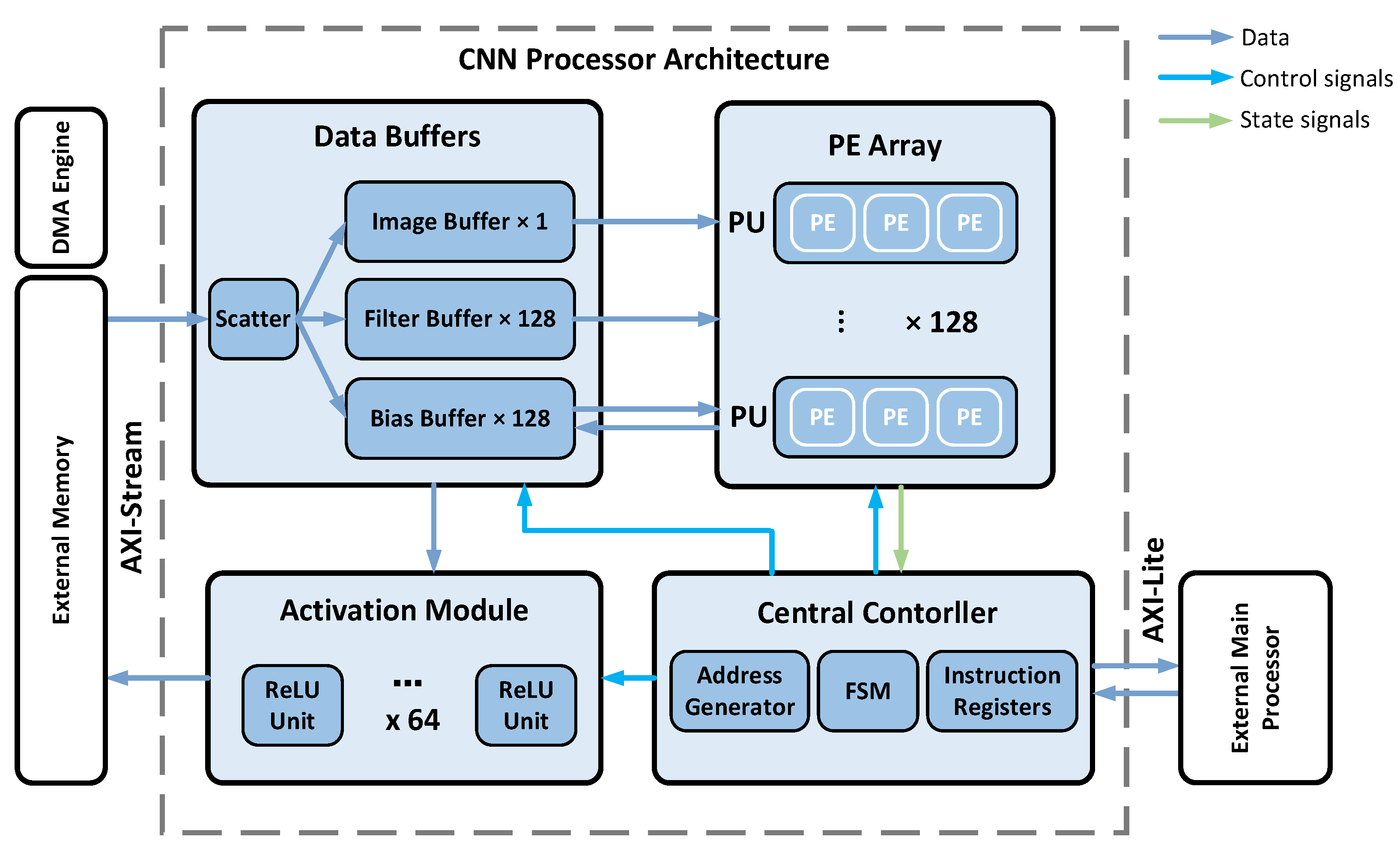
2.1. Overall Architecture of the Processor

The CNN processor architecture proposed in this paper can accelerate the computation of the convolutional layer or fully connected layer of CNNs, which is essentially equivalent to a coprocessor. The external main processor configures the instruction registers inside the processor, and direct memory access (DMA) completes the data interaction between the CNN processor and external memory.
Figure 1 illustrates the proposed CNN processor architecture, including data buffers, the computing processing element (PE) array, the activation module, the central controller and the data interface. The data buffer includes the image buffer, filter buffer and bias buffer, which are used to store image data, weight data and bias data respectively. The scatter is used to distribute the data transferred from DMA through the AXI-Stream interface to each buffer. The PE array consists of 128 processing units (PUs), and each PU is composed of a systolic array of three PEs, which is the core unit of the processor used to perform convolution and fully connected computation. The main processor configures instruction registers in the central controller through the AXI-Lite interface. The controller controls the reading and writing of each data buffer and the operation of the PE array according to the obtained configuration parameters.
In this design, the bias buffer also serves to store the intermediate values of the computing process or the final results, eliminating the need of the output buffer and saving storage resources. Such a simplified design is made possible by the systolic array computation strategy, which also makes it easier to expand the proposed processor to support parallel computing between more output feature map channels, as shown in the later sections. The first-input-first-output (FIFO) storage structure is adopted in the bias buffer to ensure first-in-first-out dataflow, and the stored computation results are carried to the external memory by DMA after the rectified linear unit (ReLU) activation.

2.2. Systolic Array-Based Computing Strategy

The systolic array represents a network of processing elements (PEs) that compute and transmit data rhythmically. These processing elements regularly input and output data to maintain regular dataflow [22]. The characteristics of the systolic array are modularization and regularization, which are very important in VLSI design.
All PEs in the systolic array are the same and work pipelined. Convolution can be completed in a systolic array. Taking a convolution operation with image size = 5 and filter size = 3 as an example, as shown in Figure 2, where i_row0–i_row4, w_row0–w_row2, b_row0–b_row2, and p_row0–p_row2 represent each row of the image values, weight values, bias values and output partial sum (psum) values, respectively, and taking p_row0 as an example, the computing process can be decomposed into:
psum00 = i_row0 ∗ w_row0 + b_row0,
psum01 = i_row1 ∗ w_row1 + psum00,
p_row0 = psum02 = i_row2 ∗ w_row2 + psum01,
where psum00(01, 02) represents the psum produced by the one-dimensional (1D) convolution of i_row0(1, 2) and w_row0(1, 2), ∗ is a convolution sign, it can be concluded that p_row1 and p_row2 have a similar computing process. These computing operations can be completed by a systolic array composed of three PEs, as shown in Figure 3. Each PE has multiplication and addition functions that can complete 1D convolution. Figure 4 shows the dataflow of a PE performing 1D convolution. The output results of each PE (such as psum00) will be temporarily stored in a FIFO as the bias values of the next PE computing. In the computing process, each row of image values is broadcast to all PEs simultaneously, and each PE completes the 1D convolution corresponding to one weight row, for example, the PE0 completes the 1D convolution of w_row0. The systolic array processing sequence is shown in Figure 5, where each dark circle represents the PE performing one 1D convolution using the corresponding image rows, weight rows and the transferred bias rows (psum rows) in unit time. The whole operation is carried out along the direction of the oblique upward arrow. Each PE obtains the psums of the previous PE from the FIFO as the bias values of its own computation. We can see from the figure that all PEs are enabled and disabled in the form of a systolic array: in t0, PE0 is enabled; in t1, PE1 is enabled; in t2, PE2 is enabled; in t3, PE0 is disabled; and in t4, PE1 is disabled; Finally, all PEs are disabled once all image rows are completed.
Table 1 shows the computation of all PEs and the results stored in FIFOs at each unit time, where psum10(11,12) represents the psum produced by the 1D convolution of i_row1(2, 3) and w_row0(1, 2), and psum20(21,22) represents the psum of i_row2(3, 4) and w_row0(1, 2). From this table we can see that the number of working PEs from t0 to t5 is 1, 2, 3, 2, 1. We can easily see that the utilization rate of the PEs in the systolic array will increase with the scale up of the input image, the majority of time all PEs are computing simultaneously in the case of a large image size. Only at the beginning and end of the convolution, the number of working PEs gradually increases from 0, then gradually decreases to 0, finally completing the convolution.
The systolic array can also easily realize the convolution with multiple input feature map channels. Taking convolution with two channels as an example, the computing process of the first channel is the same as above. For the second channel, the convolution process is similar to that shown in Figure 2, whereby the image values and weight values are changed to the second channel, while the bias values are changed to the results of the first channel, i.e., p_row0–p_row2. Similar to Equation 1, the computing process of p_row0ch2 can be decomposed into:
psum00ch2 = i_row0ch2 ∗ w_row0ch2 + p_row0,
psum01ch2 = i_row1ch2 ∗ w_row1ch2 + psum00ch2,
p_row0ch2 = psum02ch2 = i_row2ch2 ∗ w_row2ch2 + psum01ch2
where i_row0ch2–i_row2ch2 and the w_row0ch2–w_row2ch2 represent the image rows and weight rows of the second channel, respectively, and psum00(01, 02)ch2 denotes the psum produced by the convolution of i_row0(1, 2)ch2 and w_row0(1, 2)ch2. The reconfigured systolic array is shown in Figure 6a. The image rows broadcasted to PEs and the weight rows corresponding to each PE are changed to the second channel. Note that the source of bias values is changed to the FIFO2 which stores the psum rows produced by the first channel convolution. The computing process sequence of the second channel is shown in Figure 6b, which is the same as the first channel, except that the values processed are changed; thus, the control of PEs is consistent. For the case of convolution with multi-channels, the above computing rules make all other channels available and the output feature map rows are stored in FIFO2 until all channels are completed.

2.3. Analysis of the Configurability of the Systolic Array

Configurability is important to CNN processors because CNNs with various parameters can be processed by reusing the same hardware. We analyze the configurability of the systolic array in the following aspects.
(1)
Configurable image size: We can simply realize the configuration of the image size in the systolic array by broadcasting the image rows with different lengths to the PEs without changing the hardware structure.
(2)
Configurable filter size: We note that the number of PEs in the above systolic array is required to be equal to the size of the filters. For example, a systolic array with three PEs cannot complete the convolution with the filter size of five in one computing process due to an insufficient number of PEs. We can solve this problem by performing two computing processes, as shown in Figure 7. The processing sequence is horizontally split into upper and lower parts. The upper part completes the convolution of the first three weight rows, and the output intermediate values are stored in FIFO2. The lower part completes the convolution of the last two weight rows, the intermediate values stored in FIFO2 are regarded as the bias values in this process.
(3)
Configurable 3D convolution: The convolution with multiple input channels discussed in Section 2.2 is limited to the computing of one output feature map. One systolic array can complete the convolution with multiple filters serially if the time overhead is not considered. A more common method is to expand the number of systolic arrays to support parallel computing between filters, i.e., between the output feature map channels, and the operation throughput increases accordingly with the number of systolic arrays.
(4)
Fully connected computation: The fully connected computation can be regarded as a special kind of convolution due to the input image size being equal to the filter size, which can be completed by configuring the systolic array to reuse some of the PEs. For an output neuron result, only the first PE in the systolic array is needed to perform the multiplication of the image values and the weight values and accumulate the product. The operation can be expressed as follows:
OUTn = bias n + j = 1 H × W × C i j w [ n ] j
where OUTn denotes the n-th output neuron; H, W and C denote the height, width and number of channels of the input image, respectively; and ij and w[n]j denotes the j-th data of the input image and the j-th weight value of the n-th filter, respectively. Similar to convolution, fully connected computation can also use multiple systolic arrays to compute output neurons in parallel.

2.4. Analysis of the Low Power design

Hardware overhead and data access are the main sources of power consumption, and these two aspects are discussed below. We discuss the advantages of systolic arrays over other architectures in these two aspects.
(1)
Hardware overhead: According to the feature of dataflows, we can summarize acceleration into the following three categories: weight stationary (WS) [6,10,11,14], row stationary (RS) [3] and output stationary (OS) [4,5]. We take the convolution with image size = 5 and filter size = 3 as an example to evaluate the number of PEs required for each computing strategy. The WS architecture needs nine PEs due to each weight value being fixed on one PE. In the RS strategy, a 2D convolution is decomposed into many 1D convolution primitives, and each PE completes its corresponding single 1D convolution primitive, so it occupies nine PEs to meet the needs of computing. The OS architecture adopts the strategy that each PE completes the computation of a fixed output feature map value, which needs nine PEs if segmentation is not applied. The proposed strategy based on a systolic array is somewhat similar to the RS. The difference is that each PE completes all 1D convolution primitives of one weight row, so PEs are reused, and only three PEs are required to complete the 2D convolution of the example, and the power decreases accordingly with fewer PEs.
(2)
Data reuse: Supposing a PE array contains N systolic arrays composed of three PEs, since image rows are broadcast to all PEs simultaneously, image values can be reused 3 × N times. In practical applications, it is usual to use register files (RF) to temporarily store the weight rows read from SRAM for each PE in the systolic array to realize local data reuse. The weight values in RF are updated after the convolution of the current channel is completed, so the weight values are reused by (image size—filter size)/step + 1 times. In other words, it is equal to the number of rows of the output feature map. The data reuse mentioned above can effectively reduce the number of memory access, thus achieving low power in computing.

2.5. Working Process of the Processor

The interaction between the CNN processor and the external memory as well as the main processor occurs through two AXI (Advanced eXtensible Interface) interfaces, which are AXI-Stream and AXI-Lite, respectively. The working process of the processor can be divided into three parts: data preparation, computation and results output. For the convolution operation, DMA sends image data, filter data and bias data to the processor through AXI-Stream, and the data are stored in the corresponding buffer. Then, the external main processor writes instruction registers through AXI-Lite, including mode selection (convolution/fully connected computation), image size, filter size, number of channels and startup words. The convolution control finite state machine (FSM) in the controller is selected and generates control signals for PEs, and at the same time, the address generator produces addresses according to the operation parameters to read image, weight and bias data to the PE array for computation. Finally, the output feature maps are stored in the bias buffer and written back to the external memory after the activation operation.
The fully connected computation is different from the convolution operation. First, the weight data is not stored in the filter buffer because each weight data only participates in one multiplication. Second, the weight data is directly transferred to the PE array through AXI-Stream for computation, which not only reduces the computing time, but also avoids the large storage required for the weight data of the fully connected layer. Furthermore, the PUs is reconfigured to switch to the fully connected computation function. The rest of the process is similar to convolution.

3. System Modules

3.1. PE and PU

The processing element (PE) is the basic computing unit of the processor and is used to complete the multiplication and addition (MA) operations of convolution and fully connected computation. The schematic structure of the PE is shown in Figure 8a, which has two operation functions: (1) Multiply—Add: I × W + B = Psum; (2) Multiply—Accumulate: I × W + Psumi-1 = Psumi. The first function realizes the process of adding the product of the image value and weight value with the bias value transferred from outside the PE. The second function realizes the process of accumulating the product generated by the current computation with the partial sum produced by the last computation. The Sel0 and Clear signals of PE are used to switch the operation function and clear the partial sum register to zero, respectively.
Among the latest popular CNNs, the filter with a size of 3 × 3 is the most widely used. Therefore, the proposed CNN processor is mainly aimed at CNNs with filter size = 3. According to the previously mentioned computing strategy, each PE completes the 1D convolutions of one filter row, so three PEs are needed to form the systolic array, and two FIFOs are added to temporarily store the intermediate values output by PE0 and PE1, which constitutes the basic processing unit (PU) for 2D convolution, as shown in Figure 9. During the convolution process, SEL2 is configured to 0 to select the input source of the bias buffer as the output of PE2, the image buffer broadcasts image data to all PEs in the PU, each filter buffer outputs one filter row to the corresponding PE, and the bias buffer outputs the bias values to PE0. After computing starts, the PEs are enabled in the order of PE0-PE1-PE2 until all PEs are enabled, which process the 1D convolutions simultaneously, realizing the parallel operation between filter rows. The result of the current channel output from PE2 is stored in the bias buffer as the bias values for the next channel operation. After the convolution of all channels is completed, all PEs are disabled and the bias buffer stores the output feature map.
Figure 10 shows the process of the PU performing fully connected computation. We can see that only PE0 participates in the computation. At this time, SEL2 is configured as 1, and the output of PE0 is selected as the input source of the bias buffer. The final result will be directly stored in the bias buffer without being temporarily stored in FIFO0. The design of PE0 is slightly different from other PEs because it has some logic and signals related to fully connected computation. Such a PE is called Big PE, and its circuit structure is shown in Figure 8b. The Sel1 signal of the PE will be configured as 1 to directly obtain weight data from the AXI-Stream interface for computation.
The PE array in the proposed processor consists of 128 PUs, including 384 PEs. Such a design is an optimal compromise between the hardware resources available in the Xilinx ZC706 platform (AMD, Santa Clara, CA, USA) used in this paper and the throughput rate of the processor. This PE array is capable of performing parallel computation among 128 channels of the output feature map. Limited by a maximum bandwidth of 1024 bit of AXI-Stream on the ZC706 platform, the PE array is able to process the fully connected computation of 64 output neurons in parallel when the weight values are 16-bit fixed point. Of course, if we use a platform with more bandwidth and storage resources, the PE array can be scaled up to obtain a higher throughput.

3.2. Data Buffers System

The data buffers system of the processor is shown in Figure 11. All buffers interact with DDR3 by DMA through AXI4-Stream. Since the parameters of CNNs are highly reusable, the data buffers allow the data stream of the operation process to be kept mainly on-chip, avoiding frequent data exchanges with DDR3 and reducing the power of memory access. After the DMA carries data from DDR3, the scatter decides which buffer the data is sent to. This paper optimizes the storage system of the processor on the basis of making full use of bandwidth and hardware resources and maximizing the operation throughput. Table 2 shows the parameters of all data buffers in the processor.
(1)
Image buffer: The image buffer is used to transfer image data to the PE array. It consists of two levels of memory. The first level is SRAM, which can store up to 1 Mbit of image values. The second level are the register files (RF), implemented by distributed storage, which stores one image row. Compared with SRAM, RF has lower power per bit access and can, therefore, reuse image values with less energy. The data read from RF is broadcast to all PEs, and the address generator produces the read address of RF. For example, if the length of an image row is 5, the read address sequence is 1-2-3-2-3-4-3-4-5 when the convolution step is 1.
(2)
Filter buffer: Each PU has its corresponding filter buffer, which contains three sub-buffers that provide weight values to the three PEs in the PU, respectively. The sub-filter buffer also includes SRAM and RF, which can store 32 kbit weight values. Each sub-filter buffer stores one weight row in each channel of the filters that is assigned to this buffer. For example, for one conventional layer with 256 filters with a size of 3 × 3 and channels with a size of 4, each sub-filter buffer will store (256/128) × 4 = 8 weight rows, i.e., 8 × 3 = 24 values. Similar to the image data, the RF stores one row of weight values used in the current computation to achieve low power data reuse. The read addresses of all filter buffers are consistent, so only one address generator is required.
(3)
Bias buffer: The bias buffer is used to transmit bias values to the PE array and temporarily store the partial sum and the results of operation. Each PU has its corresponding bias buffer, which is composed of FIFO. There are two main reasons for this design: (1) since the computation of each output feature map only needs to add the initial bias values once, the initial bias values will no longer be used in the subsequent operation after the convolution of the first channel; and (2) according to the proposed computing strategy, the i-th psum row produced by the last channel convolution will be used as the bias values in the computation of the i-th psum row of the next channel convolution, which is consistent with the first-in-first-out rule of FIFO.

3.3. Activation Module

The nonlinear activation layer is often behind the conventional layer or the full connection layer to improve the nonlinear performance of the network. In the new DCNN model, most nonlinear activation functions adopt ReLU [23]. In this design, the operation of the PE array is based on the 16 bits signed as a fixed-point, so the ReLU function can be realized by comparing the sign bit of the input value. The ReLU function is realized by comparing the sign bit of the input value. If the sign bit is equal to 1 and the output is 0, this indicates that the value is negative; otherwise, the input value will remain unchanged and output directly. After the operation, the results in the bias buffer will be activated and then output to the external memory. Considering the maximum bandwidth of AXI-Stream on the platform, we adopt 64 ReLU function units in the activation module, which can output 64 activation results with the 16 bits fixed-point in parallel.

3.4. Central Controller

There are eight 32 bits instruction registers in the central controller, which are configured by the main processor through the AXI-Lite interface. The address and description of each register are shown in Table 3. The central controller starts the processor when it detects acc_start = f0000000 (in hex), and controls the working process according to the obtained parameters, mainly in the following three aspects: (1) configuring the PUs and controlling the enable and disable of PEs; (2) performing the data interaction between the data buffers and the PE array; (3) switching the state of computation, and controlling the activation operations to return the results through the AXI-Stream interface. The central controller has two FSMs, which are used to control the convolution and fully connected computation, respectively.

4. Hardware Implementation and Evaluation

4.1. Image Segmentation Strategy

In this paper, the performance of the processor is evaluated using the VGG-16 model. The data storage required for the computation of the first convolutional layer of VGG-16 under 16bit fixed-point quantization is at least 53 Mb, while the on-chip storage resources provided by the FPGA used in this paper are only 19.1 Mb. Therefore, the input feature map must be segmented to meet the limited on-chip resources. In this paper, the image of 13 convolutional layers of VGG-16 is segmented in three dimensions: length, width and channels. The selection of segmentation parameters needs to meet the following conditions:
L × W × C × 16 bit < imagebuf_cap,
C × (M/N) × K × 16 bit < filterbuf_cap,
(L − K + 1) × (W − K + 1) × (M/N) × 16 bit < biasbuf_cap
where L, W and C, respectively, represent the length, width and channels of the image; K and M represent the size and number of the filters, respectively; and N is the number of PUs. In this design, imagebuf_cap, filterbuf_cap and biasbuf_cap are equal to 1 Mbit, 32 kbit and 32 kbit, respectively. Table 4 shows the specific segmentation parameters.
L’, W’, and C’ are the length, width and channels of the segmented image, respectively. NL, NW, and NC are the number of segments in the three dimensions, respectively. The calculation expressions are as follows (ROUNDUP is the rounding up function):
NL = ROUNDUP((L − K + 1)/(L’ − 2)),
NW = ROUNDUP((W − K + 1)/(W’ − 2)),
NC = ROUNDUP((C − K + 1)/(C’ − 2))
The operation of the FC layer does not require image segmentation, because the capacity of the image buffer and bias buffer fully meets the operation requirements of the VGG-16 FC layer, and the weight values are directly transferred to the PE array which makes no requirement for the capacity of the filter buffer.

4.2. Hardware Verification

This paper uses the Xilinx Zynq-7000 SoC ZC706 evaluation board kit for hardware verification, as shown in Figure 12, which contains a dual-core ARM Cortex™-A9 (ARM, Cambridge, UK) processing system (PS) and an XC7Z045 FPGA programmable logic (PL). The proposed CNN processor is implemented on the PL. The software code on the PS is responsible for controlling DMA and writing operation parameters to the instruction registers. We use Xilinx Vivado (AMD, Santa Clara, CA, USA) to synthesize and lay out the processor, as shown in Figure 13.
The timing analysis result shows that the maximum clock frequency of the processor can reach 150 MHz on XC7Z045 FPGA, as shown in Figure 14. Since the multiplication and addition in PEs are pipelined operations, each PE completes two operations in each clock cycle. The mac array contains 128 PUs and has 128 × 3 = 384 PEs. When all PEs are involved in the computing, we can obtain the peak throughput as:
2 × 384 × 150 MHz = 115.2 GOP/s
The resource utilization report is shown in Figure 15. It can be seen that this design uses 530 Block RAM, with a utilization rate of 97.25%, which is as expected. The DSP utilization rate reaches 50%. The utilization of LUTRAM (mainly used for distributed storage) and FF is relatively small, being about 20%.
To estimate the power of the CNN processor, we used the Xilinx Power Estimator (XPE) (AMD, Santa Clara, CA, USA) which is a power evaluation tool provided by Xilinx. Taking the hardware utilization rate shown in Figure 15 as the evaluation indicator, the estimated on-chip power consumption is 3.801 W. We compared the performance with other CNN processors based on FPGA, as shown in Table 5, where the energy efficiency (GOP/s/W) represents the ratio of the throughput to power, and the DSP efficiency (GOP/s/DSP) represents the ratio of the throughput to DSP usage.
Thanks to computing based on a systolic array and multi-level memory that realizes the reuse of image and weight values, the proposed CNN processor achieves lower power and better energy efficiency than other designs. It also achieves a good DSP efficiency as a result of the reuse PEs in 2D convolution. In fact, the performance of the CNN processor still has much room for improvement. We find that the utilization of DSP is relatively low, which is caused by insufficient block RAM resources. If we optimize the storage structure or use a platform with more resources, the PE array can be expanded to increase the DSP utilization, so as to obtain a higher throughput.

5. Conclusions

This paper proposes an energy-efficient configurable CNN processor architecture that supports 3D convolution and fully connected computation. Thanks to the PE array composed of 128 PUs that is based on systolic array, the proposed processor implements parallel computing between filter rows in the PU and between output channels by adopting multiple PUs. Hardware and data reuse based on data broadcasting and RF storage, as well as a memory system that is suited to the dataflow of the systolic array, provide the processor with good energy efficiency and DSP efficiency. The configuration can be realized by writing the instruction registers, which enables processor supporting 3D convolutions and fully connected computation with various parameters. The application of multi-level storage structure combined with RF and SRAM in this design further reduces the power of data access. An image segmentation method is produced to run the VGG-16 model on the proposed processor to verify its functions. FPGA hardware evaluation results show that the proposed CNN processor provides comparable performance with state-of-the-art FPGA-based processors while realizing high energy efficiency.

Author Contributions

Conceptualization, C.Z. and X.W.; methodology, C.Z.; software, C.Z. and Y.Z.; validation, C.Z. and Y.Z.; formal analysis, C.Z.; investigation, C.Z. and C.W.; resources, X.W. and S.Y.; data curation, C.Z., Y.Z.; writing—original draft preparation, C.Z.; writing—review and editing, X.W. and Q.L.; visualization, C.Z.; supervision, X.W., S.Y. and Q.L.; project administration, S.Y.; funding acquisition, X.W. All authors have read and agreed to the published version of the manuscript.

Funding

This research was supported by a fundamental research grant from Shenzhen Science & Technology Innovation Commission, grant number JCYJ20200109120404043 and 2021KQNCX112.

Institutional Review Board Statement

Not applicable.

Informed Consent Statement

Not applicable.

Data Availability Statement

Not applicable.

Conflicts of Interest

The authors declare no conflict of interest.

References

  1. He, K.; Zhang, X.; Ren, S.; Sun, J. Deep Residual Learning for Image Recognition. In Proceedings of the 2016 IEEE Conference on Computer Vision and Pattern Recognition (CVPR), Las Vegas, NV, USA, 27–30 June 2016; pp. 770–778. [Google Scholar]
  2. Wang, C.-C.; Ding, Y.-C.; Chiu, C.-T.; Huang, C.-T.; Cheng, Y.-Y.; Sun, S.-Y.; Cheng, C.-H.; Kuo, H.-K. Real-Time Block-Based Embedded CNN for Gesture Classification on an FPGA. IEEE Trans. Circuits Syst. I Reg. Pap. 2021, 68, 4182–4193. [Google Scholar] [CrossRef]
  3. Chen, Y.-H.; Krishna, T.; Emer, J.S.; Sze, V. Eyeriss: An Energy-Efficient Reconfigurable Processor for Deep Convolutional Neural Networks. IEEE J. Solid State Circuits 2017, 52, 127–138. [Google Scholar] [CrossRef] [Green Version]
  4. Du, Z.; Fasthuber, R.; Chen, T.; Ienne, P.; Li, L.; Luo, T.; Feng, X.; Chen, Y.; Temam, O. ShiDianNao: Shifting vision processing closer to the sensor. In Proceedings of the ACM/IEEE 42nd Annual International Symposium on Computer Architecture (ISCA), Portland, OR, USA, 13–17 June 2015; pp. 92–104. [Google Scholar]
  5. Yin, S.; Ouyang, P.; Tang, S.; Tu, F.; Li, X.; Zheng, S.; Lu, T.; Gu, J.; Liu, L.; Wei, S. A High Energy Efficient Reconfigurable Hybrid Neural Network Processor for Deep Learning Applications. IEEE J. Solid State Circuits 2018, 53, 968–982. [Google Scholar] [CrossRef]
  6. Wong, D.L.T.; Li, Y.; John, D.; Ho, W.K.; Heng, C.-H. An Energy Efficient ECG Ventricular Ectopic Beat Classifier Using Binarized CNN for Edge AI Devices. IEEE Trans. Bio. Circuits Syst. 2022, 16, 222–232. [Google Scholar] [CrossRef] [PubMed]
  7. Yiğit, E.; Özkaya, U.; Öztürk, Ş.; Singh, D.; Gritli, H. Automatic Detection of Power Quality Disturbance Using Convolutional Neural Network Structure with Gated Recurrent Unit. Mob. Info. Syst. 2021, 2021, 7917500. [Google Scholar] [CrossRef]
  8. Peemen, M.; Setio, A.A.A.; Mesman, B.; Corporaal, H. Memory-centric processor design for Convolutional Neural Networks. In Proceedings of the 2013 IEEE 31st International Conference on Computer Design (ICCD), Asheville, NC, USA, 6–9 October 2013; pp. 13–19. [Google Scholar]
  9. Moon, S.; Lee, H.; Byun, Y.; Park, J.; Joe, J.; Hwang, S.; Lee, S.; Lee, Y. FPGA-Based Sparsity-Aware CNN Processor for Noise-Resilient Edge-Level Image Recognition. In Proceedings of the 2019 IEEE Asian Solid-State Circuits Conference (A-SSCC), Macau, China, 4–6 November 2019; pp. 205–208. [Google Scholar]
  10. Chang, X.; Pan, H.; Lin, W.; Gao, H. A Mixed-Pruning Based Framework for Embedded Convolutional Neural Network Acceleration. IEEE Trans. Circuits Syst. I Reg. Pap. 2021, 68, 1706–1715. [Google Scholar] [CrossRef]
  11. Chen, K.-C.; Huang, Y.-W.; Liu, G.-M.; Liang, J.-W.; Yang, Y.-C.; Liao, Y.-H. A Hierarchical K-Means-Assisted Scenario-Aware Reconfigurable Convolutional Neural Network. IEEE Trans. VLSI Syst. 2021, 29, 176–188. [Google Scholar] [CrossRef]
  12. Li, G.; Liu, Z.; Li, F.; Cheng, J. Block Convolution: Toward Memory-Efficient Inference of Large-Scale CNNs on FPGA. IEEE Trans. Comput. Aided Des. Integr. Circuits Syst. 2022, 41, 1436–1447. [Google Scholar] [CrossRef]
  13. Wang, J.; Fang, S.; Wang, X.; Ma, J.; Wang, T.; Shan, Y. High-Performance Mixed-Low-Precision CNN Inference Accelerator on FPGA. IEEE Micro. 2021, 41, 31–38. [Google Scholar] [CrossRef]
  14. Wu, X.; Ma, Y.; Wang, M.; Wang, Z. A Flexible and Efficient FPGA Accelerator for Various Large-Scale and Lightweight CNNs. IEEE Trans. Circuits Syst. I Reg. Pap. 2022, 69, 1185–1198. [Google Scholar] [CrossRef]
  15. Kim, T.-H.; Shin, J. A Resource-Efficient Inference Accelerator for Binary Convolutional Neural Networks. IEEE Trans. Circuits Syst. II Exp. Briefs 2021, 68, 451–455. [Google Scholar] [CrossRef]
  16. Nguyen, V.C.; Nakashima, Y. Analysis of Fully-Pipelined CNN Implementation on FPGA and HBM2. In Proceedings of the Ninth International Symposium on Computing and Networking Workshops (CANDARW), Matsue, Japan, 23–26 November 2021; pp. 134–137. [Google Scholar]
  17. Jiang, J.; Jiang, M.; Zhang, J.; Dong, F. A CPU-FPGA Heterogeneous Acceleration System for Scene Text Detection Network. IEEE Trans. Circuits Syst. II Exp. Briefs 2022, 69, 2947–2951. [Google Scholar] [CrossRef]
  18. Guo, Y.; Jiang, M.; Dong, F.; Yu, K.; Chen, K.; Qu, W.; Jiang, J. A CPU-FPGA Based Heterogeneous Accelerator for RepVGG. In Proceedings of the IEEE 14th International Conference on ASIC (ASICON), Kunming, China, 26–29 October 2021; pp. 1–4. [Google Scholar]
  19. Cavigelli, L.; Benini, L. Origami: A 803-GOP/s/W Convolutional Network Processor. IEEE Trans. Circuits Syst. Video Technol. 2017, 27, 2461–2475. [Google Scholar] [CrossRef] [Green Version]
  20. Sankaradas, M.; Jakkula, V.; Cadambi, S.; Chakradhar, S.; Durdanovic, I.; Cosatto, E.; Graf, H.P. A Massively Parallel Coprocessor for Convolutional Neural Networks. In Proceedings of the 2009 20th IEEE International Conference on Application-Specific Systems, Architectures and Processors, Boston, MA, USA, 7–9 July 2009; pp. 53–60. [Google Scholar]
  21. Luo, T.; Liu, S.; Li, L.; Wang, Y.; Zhang, S.; Chen, T.; Xu, Z.; Temam, O.; Chen, Y. DaDianNao: A Neural Network Supercomputer. IEEE Trans. Comput. 2017, 66, 73–88. [Google Scholar] [CrossRef]
  22. O’Leary, D.P. Systolic Arrays for Matrix Transpose and Other Reorderings. IEEE Trans. Comput. 1987, C–36, 117–122. [Google Scholar] [CrossRef]
  23. Qiu, S.; Xu, X.; Cai, B. FReLU: Flexible Rectified Linear Units for Improving Convolutional Neural Networks. In Proceedings of the 24th International Conference on Pattern Recognition (ICPR), Beijing, China, 20–24 August 2018; pp. 1223–1228. [Google Scholar]
  24. Qiu, J.; Wang, J.; Yao, S.; Guo, K.; Li, B.; Zhou, E.; Yu, J.; Tang, T.; Xu, N.; Song, S.; et al. Going Deeper with Embedded FPGA Platform for Convolutional Neural Network. In Proceedings of the ACM/SIGDA International Symposium on Field-Programmable Gate Arrays, Monterey, CA, USA, 21 February 2016; pp. 26–35. [Google Scholar]
  25. Liang, Y.; Lu, L.; Xiao, Q.; Yan, S. Evaluating Fast Algorithms for Convolutional Neural Networks on FPGAs. IEEE Trans. Comput. Aided Des. Integr. Circuits Syst. 2020, 39, 857–870. [Google Scholar] [CrossRef]
  26. Li, X.; Huang, H.; Chen, T.; Gao, H.; Hu, X.; Xiong, X. A hardware-efficient computing engine for FPGA-based deep convolutional neural network accelerator. Microelectron. J. 2022, 128, 105547. [Google Scholar] [CrossRef]
  27. Guo, K.; Sui, L.; Qiu, J.; Yu, J.; Wang, J.; Yao, S.; Han, S.; Wang, Y.; Yang, H. Angel-Eye: A Complete Design Flow for Mapping CNN Onto Embedded FPGA. IEEE Trans. Comput. Aided Des. Integr. Circuits Syst. 2018, 37, 35–47. [Google Scholar] [CrossRef]
Figure 1. Proposed CNN processor architecture.
Applsci 12 12633 g001
Figure 2. Example of a convolution operation.
Applsci 12 12633 g002
Figure 3. Systolic array composed of three PEs.
Applsci 12 12633 g003
Figure 4. Dataflow of a PE performing 1D convolution.
Applsci 12 12633 g004
Figure 5. Processing sequence of the systolic array in the convolution.
Applsci 12 12633 g005
Figure 6. (a) Reconfigured systolic array; (b) processing sequence of convolution in the second channel.
Applsci 12 12633 g006
Figure 7. Convolution in two processing sequences. In this example, image size = 8, filter size = 5, step = 1, mp_row0–mp_row3 denote the intermediate psum rows produced in process 1, and p_row0–p_row3 denote the psum rows of the results. The unit times in process 2 are indicated in light blue.
Applsci 12 12633 g007
Figure 8. (a) Schematic of the PE; (b) schematic of the Big PE.
Applsci 12 12633 g008
Figure 9. Diagram of the PU performing the convolution operation.
Applsci 12 12633 g009
Figure 10. Diagram of the PU performing fully connected computation.
Applsci 12 12633 g010
Figure 11. Diagram of the data buffers system.
Applsci 12 12633 g011
Figure 12. ZC706 evaluation board.
Applsci 12 12633 g012
Figure 13. Layout of the proposed CNN processor.
Applsci 12 12633 g013
Figure 14. Timing analysis report.
Applsci 12 12633 g014
Figure 15. Resource utilization report.
Applsci 12 12633 g015
Table 1. Computation of PEs and the results stored in FIFOs.
TimePE0FIFO0PE1FIFO1PE2FIFO2
t0i_row0 ∗ w_row0 + b_row0psum00
t1i_row1 ∗ w_row0 + b_row1psum10i_row1 ∗ w_row1 + psum00psum01
t2i_row2 ∗ w_row0 + b_row2psum20i_row2 ∗ w_row1 + psum10psum11i_row2 ∗ w_row2 + psum01psum02
(p_row0)
t3 i_row3 ∗ w_row1 + psum20psum21i_row3 ∗ w_row2 + psum11psum12
(p_row1)
t4 i_row4 ∗ w_row2 + psum21psum22
(p_row2)
Table 2. Parameters of the data buffers.
BufferBit Width (Bits)Storage StructureCapacity (Bits)Number
Image Buffer16SRAM + RF1 M1
Filter Buffer163 SRAM + 3 RF3 × 32 K128
Bias Buffer16FIFO32 K128
Table 3. Description of the instruction registers.
RegistersAddress (In Hex)DirectionDescription
input_channel00InputNumber of input channels
output_channel04InputNumber of output channels
ifmap_size08InputInput feature map size
filter_size0CInputFilter size
convfc_sel10InputCONV/FC selection 1
base_addr14InputImage values base address
acc_start18InputOperation start: f0000000
complete_fb1COutputOperation completion feedback
1 CONV: convolution; FC: fully connected computation.
Table 4. Segmentation parameters of each convolutional layer of VGG-16.
CONV LayerImage SizeL’NLW’NWC’NC
CONV1224 × 224 × 334734731
CONV2224 × 224 × 64347347641
CONV3112 × 112 × 64344344641
CONV4112 × 112 × 1283443441281
CONV556 × 56 × 1282232231281
CONV656 × 56 × 2562232232561
CONV756 × 56 × 2562232232561
CONV828 × 28 × 2561821821282
CONV928 × 28 × 5121821821284
CONV1028 × 28 × 5121821821284
CONV1114 × 14 × 5121411411284
CONV1214 × 14 × 5121411411284
CONV1314 × 14 × 5121411411284
Table 5. Performance comparison with state-of-the-art CNN processors.
Reference[24][25][26][27][2]This Work
PlatformZynq
ZC706
Zynq
ZC706
Zynq
ZC706
Zynq
XC7Z020
Arria 10
GX1150
Zynq
ZC706
Frequency (MHz)150166200214240150
Technology28 nm28 nm28 nm28 nm20 nm28 nm
Precision16 bits fixed16 bits fixed16 bits fixed8 bits fixed16 bits fixed16 bits fixed
Throughput (GOP/s)136.97201.1107.984.3968.03115.2
Power (W)9.639.46.233.5403.8
Energy EFF (GOP/s/W)14.2221.3917.3224.0924.2030.32
DSP Used9009004485713136449
DSP EFF (GOP/s/DSP)0.150.230.240.150.300.26
Publisher’s Note: MDPI stays neutral with regard to jurisdictional claims in published maps and institutional affiliations.

