Communication

Joule-Heating Annealing to Increase Organic Solar Cells Performance: A Comparative Study

by
Maria Méndez
1,2,†,
Daniel Fernández
1,
Aurelien Viterisi
3,
Eugenia Martínez-Ferrero
1,2,*,† and
Emilio Palomares
1,4,*
1
Institute of Chemical Research of Catalonia (ICIQ-BIST), Avda. Països Catalans, 16, 43007 Tarragona, Spain
2
EURECAT, Centre Tecnològic de Catalunya, Avda. Ernest Lluch 36, 08302 Mataró, Spain
3
IPREM UMR5254—UPPA/CNRS, Technopole Hélioparc, 2 Avenue du Président Pierre Angot, 64053 Pau, France
4
Catalan Institution for Research and Advanced Studies (ICREA), 08010 Barcelona, Spain
*
Authors to whom correspondence should be addressed.
Currently at ICIQ.
Appl. Sci. 2022, 12(5), 2552; https://doi.org/10.3390/app12052552
Submission received: 27 January 2022 / Revised: 23 February 2022 / Accepted: 24 February 2022 / Published: 28 February 2022
(This article belongs to the Special Issue Organic and Hybrid Photovoltaics)

Abstract

:
In this work, we present our results on the influence of post-deposition treatments on the morphology and optical properties of photoactive films made of small molecules and their subsequent effect on the performance of photovoltaic (PV) devices. We have chosen DPP(TBFu)2:PC61BM as a benchmark model system and compared a novel joule-heating annealing (JHA) treatment with the widely used temperature annealing (TA) and solvent annealing (SVA) treatments. Detailed characterization of the morphology of the active layer and the performance of the devices suggests that JHA is a valuable post-treatment technique that provides fast information about the development of domains in the photoactive layer. Finally, in this context, solar cells on flexible indium tin oxide (ITO) substrates, made of polyethylene terephthalate (PET), were fabricated and analyzed.

Graphical Abstract

1. Introduction

Research in solar energy harvesting has seen extraordinary development since the emergence of hybrid perovskite solar cells [1,2]. However, despite the tremendous advance in perovskite-based solar cells, organic solar cells (OSCs) are still receiving much attention [3], especially after their progress in terms of power conversion efficiency (PCE) over 18% [4]. These late record values make them competitive with other photovoltaic technologies. Furthermore, progress has also been achieved on stability, processing of large active areas, and material development [3]. Consequently, OSCs show a stronger potential for industrialization than other techniques, such as less energy-demanding device fabrication, easy recyclability, and the absence of toxic elements in their basic structure. Nevertheless, while OSC efficiency is often compared with existing and mature photovoltaic technologies manufactured industrially, there are few reports on the industrialization of active layer deposition that still requires posterior treatments to optimize its activity [5,6,7,8].
Organic solar cells made of π-conjugated semiconducting polymers and fullerene derivatives have led the race for champion solar cells during the last decades due to their performance and facile fabrication by means of solution-processed technologies. In fact, donor polymers with “donor-acceptor” alternating motifs (i.e., electron-donating and electron-withdrawing building blocks) superseded the classical approach to polymer design. Similarly, traditional fullerene-based electron acceptors [9] were more recently replaced by non-fullerene materials. However, the batch-to-batch reproducibility of polymers still limits their application on an industrial scale [5]. On the contrary, small-molecule donors possess the advantage of having a well-defined molecular weight, easy purification steps, and little batch-to-batch variations [10,11]. Among the myriad of available molecular structures, diketopyrrolopyrrole (DPP) is a typical industrial pigment chromophore with a high optical density. It has been widely used as a building block in the design of donor molecules due to its facile synthesis from low-cost starting materials, strong electron affinity that enables lower frontier energy levels, and ease of structural modification, which allows for tailored optoelectronic properties. The DPP unit can be combined with other molecular units to form a “donor-acceptor-donor” structure [12] that enhances its potential for photovoltaic applications. This is the case, for example, of the 3,6-bis(5-(benzofuran-2-yl) thiphen-2-yl) -2,5-bis (2-ethylhexyl) pyrrolo [3,4-c] pyrrole-1,4-dione molecule (DPP(TBFu)2) that can form part of solar cells when mixed with PC71BM as an acceptor, giving 4.4% power conversion efficiencies (PCE) [13]. The combination of the morphology at the nanoscale, phase separation, moderate mobility of the holes, and the relatively high Voc account for the obtained PCE value.
Due to the opportunities offered by the DPP, the commercial availability of the components, and the simplicity of the device composition, we have selected the DPP(TBFu)2:PC61BM system (see Figure 1 for the molecular structures) as a benchmark model to study the effects of three different post-deposition treatments on the PCE of the PV devices. As-cast photoactive films often exhibit poor device performance and require subsequent processing to improve their efficiency. Post-deposition treatments are vital for molecular ordering at the nanoscale and are a key factor in the achievement of high fill factors (FFs) and high PCEs. The post-deposition treatment processes influence the intra- or intermolecular weak interactions (essentially π-π stacking) leading to the formation of well-ordered crystalline domains [14]. The molecular ordering increases the degree of donor and acceptor phase separation, enhancing charge transport and reducing charge recombination. The post-deposition treatment determines the length scale of phase separation as well, which is critical for exciton dissociation and charge transport. If the length scale is too large, excitons may recombine before reaching the interface between donor and acceptor phases, while reduced phase separation impedes efficient charge transport. In fact, domain sizes of 20 nm in bulk heterojunction (BHJ) materials are optimum for charge separation and transport because the exciton diffusion length is about 10 nm [13]. In this work, we have selected well-known post-treatment strategies, such as thermal annealing (TA), exposure of the organic layer to a saturated solvent vapor (solvent vapor annealing, SVA), and the less known joule-heating annealing (JHA). To the best of our knowledge, JHA, consisting of applying a current bias to the device, has been mainly applied to improve the electrical and thermal properties of inorganic materials but has not been previously used to improve the crystallinity of the active layer [15,16]. Finally, we selected polyethylene terephthalate (PET) as a flexible substrate. Flexibility and lightweightness are two of the major advantages that OSCs present over traditional silicon solar cells. Moreover, in comparison to other existing substrates, such as polyimide or polyethylene naphtalate, PET is the substrate of choice for most solar cell manufacturers due to its mechanical properties, excellent transparency, and solvent resistance combined with its low price [17]. Consequently, we have also studied the impact of using PET on the performance of the DPP(TBFu)2:PC61BM system.

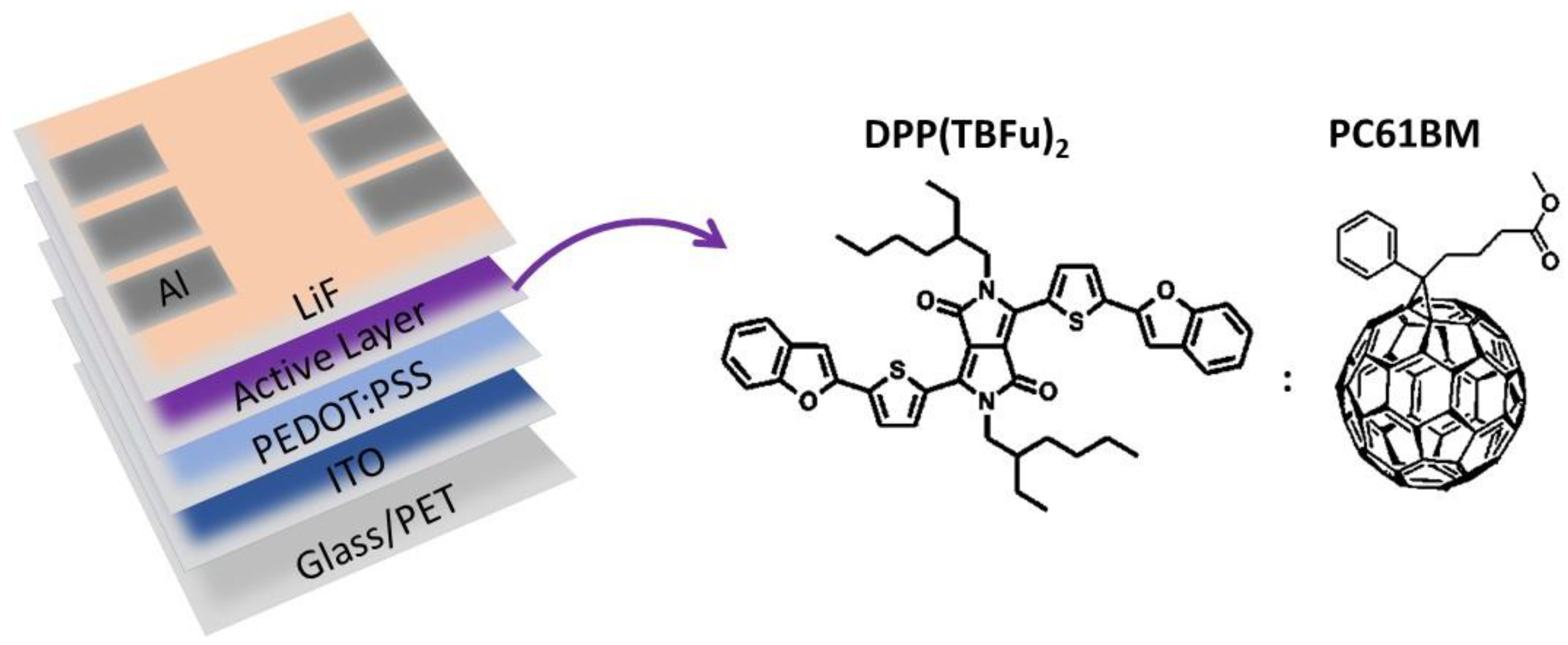
2. Materials and Methods

Materials:
DPP(TBFu)2 and PC61BM were purchased from Luminescence Technology Corp. and from SOLENNE (99.5%), respectively. The solvents used are: CHCl3 (99.8%, Sigma-Aldrich, St. Louis, MO, USA) for the active layer deposition, THF (>99.9%, Sigma Aldrich) and CH2Cl2 (>99.8%, DCM, Sigma-Aldrich) for the SVA treatment. Aluminum (99.99%) and LiF (99.995%) were purchased from Kurt J. Lesker-Materials Group and Sigma-Aldrich, respectively. Pre-patterned Indium Tin Oxide (ITO) on glass and on PET were purchased from PsioTec and Visiontek, respectively.
Device preparation:
First, the substrates that were treated identically were rinsed with acetone to remove the residual photoresist layer. The substrates were then placed in a glass holder and sequentially sonicated in acetone for 10 min and in isopropanol twice for 10 min. Finally, the substrates were ozone-treated in a homemade system for 45 min, and subsequently spin coated in air with a layer of sonicated and filtered (0.45 μm, cellulose acetate) solution of poly(3,4-ethylenedioxythiophene):poly(styrene sulfonate) (PEDOT:PSS, Orgacon IJ−1005) at 8000 rpm for 90 s and using an acceleration of 4320 rps. The PEDOT:PSS film was dried at 120 °C under an inert atmosphere for 30 min. The active layer was dissolved in CHCl3 and spin coated in air over the PEDOT:PSS layer from a 20 mg·ml−1 (total concentration in CHCl3) solution of DPP(TBFu)2 and PC61BM (6:4 w/w ratio) in a bulk heterojunction (BHJ) way [18]. The spin-coating conditions were adapted to obtain a layer thickness of 100 nm. The post-fabrication treatment was carried out straight after deposition of the active layer:
  • Solvent vapor annealing (SVA) was achieved by exposing the films to a saturated vapor of solvent of THF or DCM in an airtight vessel [19]. The vessel (200 mL) was filled with 7 mL of an organic solvent and left sealed for 5 min prior to the SVA step to ensure that the headspace was saturated with the solvent. The substrates were exposed to the solvent vapors until the color of the films changed (between 1 and 2 min).
  • Thermal annealing (TA) was done on a heating plate at 65−110 °C until the color changed.
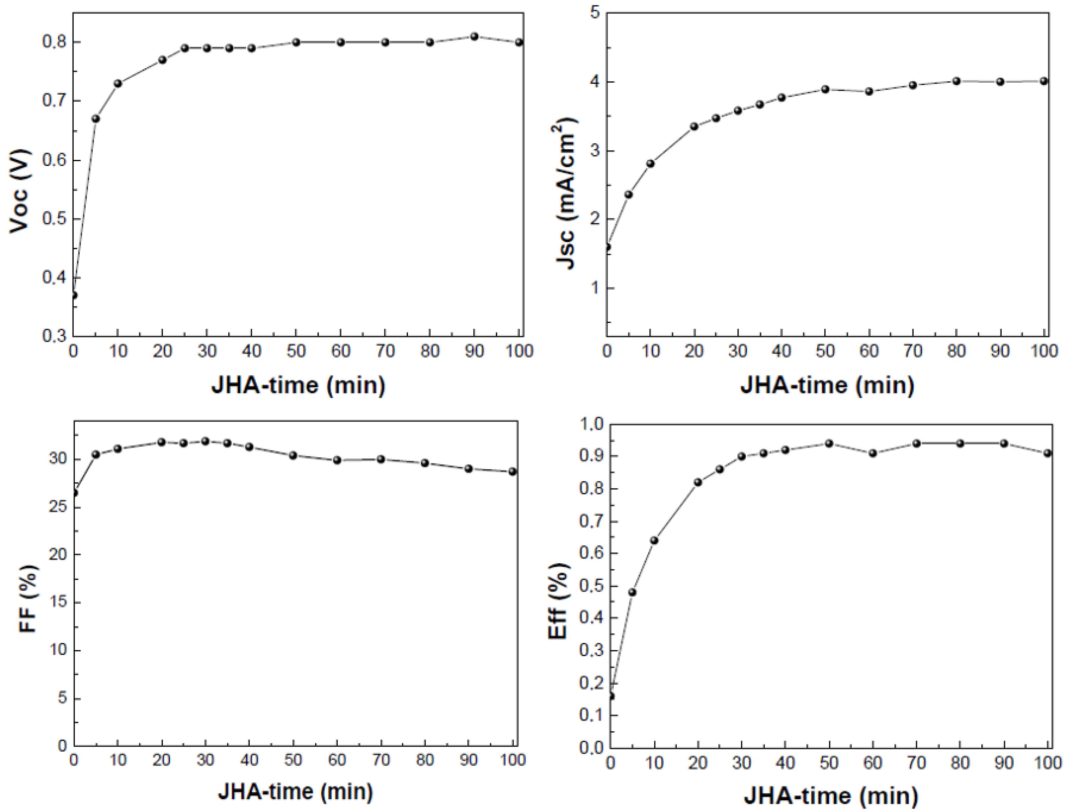
  • Joule-Heating-Annealing (JHA) was also explored. This treatment is based on the heat released by the flow of an electric current generated after application of a constant voltage through the metallic contacts of the devices. The domains are formed by means of increasing the temperature due to the current flow through the active layer. The constant voltage applied was 5 V, and the current observed was 30–40 mA.
Finally, the cathode layer was deposited by thermal evaporation in an ultra-high vacuum chamber (<1 × 10⁻⁶ mbar). Metals were evaporated through a mask leading to devices with an area of 25 mm2. LiF (1 nm) and Al (100 nm) were deposited at a rate of 0.1 Å·s−1 and 0.5 Å·s−1, respectively.
Characterization:
The UV-Vis absorption of the films was measured using a PerkinElmer spectrophotometer (Lambda 950). The J-V characteristics of the devices were measured in an ambient atmosphere using an ATLAS Solar Simulator without the use of encapsulating layers. The illumination intensity was measured to be 100 mW·m2 with a calibrated Pyranometer CMP6 with a sensitivity of 18.76·10−6 V/W·m−2 and a METEON Irradiance Meter. The applied potential and cell current were measured with a Keithley 2602A System digital source meter. The photocurrent and irradiated light intensity were measured simultaneously and processed with home-built Labview© software. The thickness and roughness of the films were measured with a stylus profilometer Veeco (Dektak 150) from a scratch applied in the center of the film. Atomic Force Microscopy was used mainly to study the roughness of the active layer but also to observe the different morphology of the donor/acceptor domains. AFM of the samples was performed in tapping mode on a Molecular Imaging model Pico SPM II (pico+). AFM images were collected in air using silicon probes with a typical spring constant of 1–5 nN·m−1 and at a resonant frequency of 75 kHz.

3. Results and Discussion

First, reference devices were fabricated to compare the PCE obtained in this work with those reported in the literature. Therefore, devices with the structure glass/ITO/PEDOT:PSS/active layer(BHJ)/LiF/Au with 9 cm2 active layer area were fabricated. The best results (champion cell) showed a PCE of 4.42% with a Voc of 0.808 V, Jsc of 15.39 mA/cm2, and FF of 35.6 (see Figure S1). The efficiencies obtained in this work for the reference cell were equivalent in comparison to the values reported in the literature [13,18]. It is important to note that except for the reference cell, the active layer area used in this work was 25 cm2 for all the devices, which is considered much larger than the area usually reported in the literature.

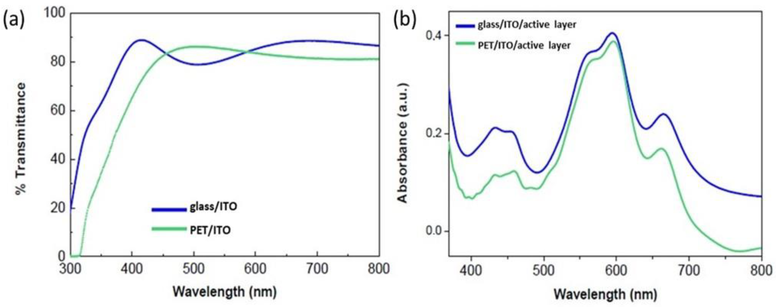
3.1. The Effects of Using PET

Table 1 summarizes the main properties of both commercial ITO substrates employed in this work. To preserve their mechanical properties, the ITO films in flexible substrates are thinner in comparison with those on ITO-glass. This causes significant differences in sheet resistance and average roughness values.
Table 2 shows the results of devices prepared on both types of substrates under identical experimental conditions (see Materials and Methods) and after using thermal annealing at 110 °C as post-fabrication treatment. As expected, SM-BHJ solar cells fabricated on ITO-PET showed lower performance than those fabricated on ITO-glass. Several reasons account for these differences. First, it has been reported that the PCE decreases as ITO surface roughness increases, influencing cell performance and even causing short circuits [20]. This observation agrees with our results since the roughness of the ITO-PET substrate is five times higher than that of the glass-based film (see Table 1). Second, we measured the optical transmittance of the substrates in the wavelength range of 300–800 nm. As can be seen in Figure 2a the comparison of the area under the curve indicates that ITO-PET substrate shows 11% less transmittance than ITO-glass, which is assigned to the higher roughness of the flexible ITO surface that scatters more light, and to the lower transmittance of the PET substrate at wavelengths under 420 nm and above 600 nm. This difference is also seen in the UV-Visible spectra for the partially fabricated solar cell devices (see Figure 2b), where the molecules deposited onto the flexible substrate absorb less light than those on glass. The differences in light absorption are reflected in the lower photogenerated Jsc of the flexible devices (see Table 2).
On the other hand, Ajuria et al. [21] attributed the low fill factor and/or a non-optimized charge transport due to unbalanced charge carrier mobility. Additionally, Street et al. [22] recognized sheet resistance (Rs) as one of the key parameters affecting the performance of organic photovoltaic devices through reduction of the FF. In fact, this suits well with the results observed in our devices since the PET-based devices with higher Rs showed lower FF. It is worth noting that the Rs is related to the energy loss in carrier transport and is strongly affected by the interfacial barriers crossed by charges in their way to the electrodes. This includes the ohmic contributions of the electrodes, the contact between the organic semiconductor and the metal, and the resistance of the active materials. Comparably, the parallel resistance (Rp) illustrates the potential leakage current through the device and around the edges of the active area. Transparent contact layers, such as indium tin oxide ITO, and carrier transporting interlayers of different kinds could increase Rs significantly [23]. In general, these layers may add more resistance because of less-than-optimum energy level alignment and differences in polarity, which affects interfacial charge transfer. Therefore, we believe that the higher Rs and Rp values in the flexible substrates are the origin of the lower Voc and FF, and consequently lower device performances. However, these observations are, by no means, affecting the purpose of this study on the impact of post-deposition treatment on PV characteristics.

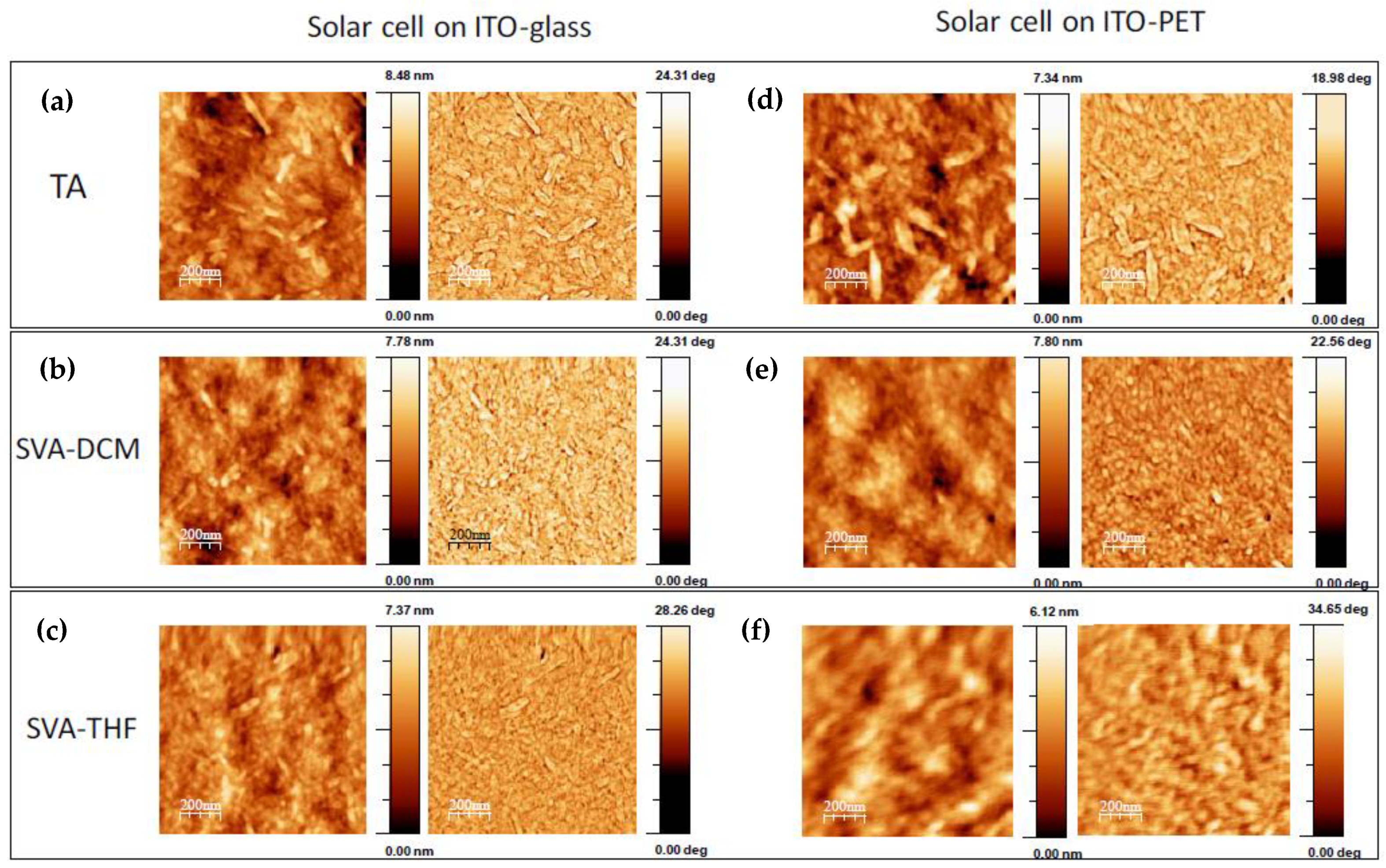
3.2. Post-Treatment of the Active Layer

In this work, we used three different post-treatments: thermal annealing (TA), solvent vapor annealing (SVA), and joule-heating annealing (JHA). On the one hand, TA is easy to apply, but on the other hand, it is limited by the difficulties inherent in achieving high heating or cooling rates, since heat must transfer throughout the sample by thermal conduction [24]. Moreover, extended thermal annealing has been shown to create large crystals, from a few to up to 100 μm, that could be detrimental to the performance of the device [25]. Additionally, many cracks can be generated in the ITO/PET interface during the TA process due to the lower thermal stability of PET compared to glass [26].
On the other hand, SVA is a versatile method where thin films are exposed to an atmosphere saturated with solvent vapors in which the solid film constituents are soluble. The solvent molecules diffuse into the deposited layer, the extent of which is dependent on, and thus controllable, the solubility and exposure time. However, the application of SVA to large areas is more difficult in comparison to TA, especially when dealing with high throughput opened processing. For the TA treatment, a range of temperatures between 65 and 110 °C was applied to the samples by using a hotplate. The treatment temperature was first set to 110 °C and later reduced to 65 °C after the results obtained by JHA (vide infra). The SVA processing was done with dichloromethane (SVA-DCM) and tetrahydrofuran (SVA-THF) to compare chlorinated and non-chlorinated solvents. For both techniques, the most convenient way to stop the treatment was to follow the color change from blue to purple (Figure S2), since it marked the formation of more ordered domains between the donor and acceptor.
Figure 3 shows the AFM images of the devices annealed using TA and SVA treatments on glass and on PET substrates. For the two different substrates, the devices annealed using the TA treatment (Figure 3a,b) display larger rod-domains than the devices annealed by SVA (Figure 3b,c,e,f), which showed similar size and more homogeneous round-shape domains. The bright dots observed in the phase images are due to PC61BM, which has a higher elastic (Young’s) modulus [27]. It is noteworthy to observe that, while the roughness of the ITO on PET is higher than the roughness of the ITO on glass, after spin-coating and post-deposition annealing treatment of the photoactive layer, the final roughness of this layer is no longer dependent on the roughness of the ITO substrate. The results of the AFM image analysis show that the dimensions of domains are affected by the post-treatment technique and the annealing time. Thus, the domains for the samples treated by TA are about 200 nm, whereas those treated by SVA (for both DCM and THF solvents) are found to be below 100 nm. Treatment time is also a crucial parameter, and when a sample was overexposed to SVA, the domain size increased significantly up to 300 nm (Figure S3).
Regarding the SVA-treated films, similar results were observed by absorption spectroscopy. The films show an increase in the absorption intensity after exposure to either DCM or THF, with this effect slower on THF-treated samples (Figure S4). In addition, there is a shift in the absorbance maximum from 605 nm to 595 nm, pointing to an increase in the domain size [19]. The characteristics of the devices exposed during different times are shown in Table 3. DCM has been selected as an example since the effect of non-chlorinated THF is similar. The cell performance trend is similar in both ITO-glass and ITO-PET, pointing to an optimum time for SVA post-treatment of 2 min. At longer times, all the parameters decrease progressively. The increase in domain size presumably promotes the geminate recombination of charge carriers with a subsequent decrease of photogenerated current, Voc and FF.
Figure 4 and Figure S5a shows the results of the JHA treatment. The cell performance improves exponentially during the first 20 min of treatment, where the PCE is seen to increase six-fold. After 20 min, the Voc and Jsc remain stable, but the FF decreases, probably due to resistive losses. This behavior is assigned to the increase of the nanodomains of the active layer that result in the initial enhancement of the Jsc and Voc. However, the extent to which the JHA can be used to increase the size of the domains is limited in contrast to the other post-deposition techniques. SVA and the thermal treatment can induce a continuous growth of the crystal domains, which, at the beginning, has a faster effect on the performance, mainly due to an increase in the film crystallinity [19], but a faster detrimental effect as well because of the increase in the charge recombination. However, JHA has a smoother effect, which is also limited by the value of the applied current, and thus, the growth of the domains can be controlled.
The post-deposition treatment was studied on flexible devices due to their potential and ease of application on roll-to-roll coating systems. The average temperature was measured by using a thermal camera under operating conditions (see Figure S5b). The thermographic image indicates that the cell reached temperatures between 65 and 80 °C, which is compatible with flexible substrates. With this data, we adapted the thermal annealing modified from 110 °C to 65 °C, keep it for 5 min at 65 °C and then up to 80 °C annealing until the color changes from blue to purple, obtaining better results (see Table 4). Therefore, the JHA might be used to find the optimal annealing temperature since this is a post-treatment that can be applied ‘in operando’ conditions. We could also confirm that the changes induced by JHA are not reversible and that they are not related to any excess or saturation of charges, as can be observed in other kinds of solar cells as a ‘light soaking’ effect [28,29].

4. Conclusions

In summary, we compared three post-deposition processing treatments using DPP(TBFu)2:PC61BM as a model system. First, we determined that the decrease in PCE in flexible ITO-PET substrates was mainly due to the characteristics of the ITO film. Therefore, we consider it of high importance to find new flexible architectures that conjugate the ITO properties while maintaining the mechanical qualities of the substrate. Then, we tested several post-deposition processing treatments for the active layer, among which JHA is described for the first time for the annealing of the photoactive layer in this kind of device. On one hand, TA and SVA are widely used techniques and showed comparable efficiency results in this work. However, the testing of several exposure times and additional characterization is required to optimize device fabrication. On the other hand, the application of JHA provides a precise temperature treatment that has allowed us to tune the regular thermal annealing processing and increase the PCE of the devices (50% higher). Moreover, it is readily applied and has given excellent results in shorter times in comparison to the other two techniques.
Finally, we believe that these results can be of interest for the post-deposition treatment of larger-area devices, especially the JHA treatment, since it is applied in in-operando conditions. With JHA, the improvement in the photoactive domains can be monitored in real time, allowing for easier optimization during the device fabrication process.

Supplementary Materials

The following are available online at https://www.mdpi.com/article/10.3390/app12052552/s1, Figure S1. J-V curve of the reference cell with the following structure: glass/ITO/PEDOT:PSS/active layer/LiF/Au. Figure S2. Photographs of DPP(TBFu)2:PCBM films as-casted (blue) and after SVA treatment (purple) made in a close home-made system. Figure S3. (a). AFM images and (b) roughness profile of a sample overexposed to a SVA treatment. Figure S4. Absorption spectra of as-cast and solvent vapour annealed devices on glass for different times when using (a) DCM and (b) THF. Figure S5. (a) J-V curves of a flexible device under JHA treatment from as-cast to 90 minutes and (b) image taken by a thermal camera during the application of the JHA on a solar cell.

Author Contributions

Conceptualization, M.M., E.M.-F. and E.P.; methodology M.M., D.F., A.V.; validation M.M., D.F., A.V., E.M.-F. and E.P., writing – original draft, review and editing M.M., D.F., A.V., E.M.-F., E.P., Supervision E.M.-F., E.P. All authors have read and agreed to the published version of the manuscript.

Funding

This research was funded by Eurecat, ICIQ, ICREA and AGAUR grant number 2017-SGR-978.

Institutional Review Board Statement

Not applicable.

Informed Consent Statement

Not applicable.

Data Availability Statement

Not applicable.

Acknowledgments

The authors acknowledge funding from Eurecat, ICIQ, and ICREA. AGAUR is also acknowledged for financial support through project 2017-SGR-978.

Conflicts of Interest

The authors declare no conflict of interest.

References

  1. A decade of perovskite photovoltaics. Nat. Energy 2019, 4, 1. [CrossRef] [Green Version]
  2. Jeong, J.; Kim, M.; Seo, J.; Lu, H.; Ahlawat, P.; Mishra, A.; Yang, Y.; Hope, M.A.; Eickemeyer, F.T.; Kim, M.; et al. Pseudo-halide anion engineering for α-FAPbI3 perovskite solar cells. Nature 2021, 592, 381–385. [Google Scholar] [CrossRef] [PubMed]
  3. Wu, J.; Gao, M.; Chai, Y.; Liu, P.; Zhang, B.; Liu, J.; Ye, L. Towards a bright future: The versatile applications of organic solar cells. Mater. Rep. Energy 2021, 1, 100062. [Google Scholar] [CrossRef]
  4. Liu, F.; Zhou, L.; Liu, W.; Zhou, Z.; Yue, Q.; Zheng, W.; Sun, R.; Liu, W.; Xu, S.; Fan, H.; et al. Organic Solar Cells with 18% Efficiency Enabled by an Alloy Acceptor: A Two-in-One Strategy. Adv. Mater. 2021, 33, 2100830. [Google Scholar] [CrossRef] [PubMed]
  5. Burgués-Ceballos, I.; Stella, M.; Lacharmoise, P.; Martínez-Ferrero, E. Towards industrialization of polymer solar cells: Material processing for upscaling. J. Mater. Chem. A 2014, 2, 17711–17722. [Google Scholar] [CrossRef]
  6. Lucera, L.; Kubis, P.; Fecher, F.W.; Bronnbauer, C.; Turbiez, M.; Forberich, K.; Ameri, T.; Egelhaaf, H.-J.; Brabec, C.J. Guidelines for Closing the Efficiency Gap between Hero Solar Cells and Roll-To-Roll Printed Modules. Energy Technol. 2015, 3, 373–384. [Google Scholar] [CrossRef]
  7. Strohm, S.; Machui, F.; Langner, S.; Kubis, P.; Gasparini, N.; Salvador, M.; McCulloch, I.; Egelhaaf, H.-J.; Brabec, C.J. P3HT: Non-fullerene acceptor based large area, semi-transparent PV modules with power conversion efficiencies of 5%, processed by industrially scalable methods. Energy Environ. Sci. 2018, 11, 2225–2234. [Google Scholar] [CrossRef]
  8. Liu, C.; Xiao, C.; Xie, C.; Li, W. Flexible organic solar cells: Materials, large-area fabrication techniques and potential applications. Nano Energy 2021, 89, 106399. [Google Scholar] [CrossRef]
  9. Cambarau, W.; Fritze, U.F.; Viterisi, A.; Palomares, E.; von Delius, M. Increased short circuit current in an azafullerene-based organic solar cell. Chem. Commun. 2015, 51, 1128–1130. [Google Scholar] [CrossRef] [Green Version]
  10. Zhou, R.; Jiang, Z.; Yang, C.; Yu, J.; Feng, J.; Adil, M.A.; Deng, D.; Zou, W.; Zhang, J.; Lu, K.; et al. All-small-molecule organic solar cells with over 14% efficiency by optimizing hierarchical morphologies. Nat. Commun. 2019, 10, 5393. [Google Scholar] [CrossRef]
  11. Collins, S.D.; Ran, N.A.; Heiber, M.C.; Nguyen, T.-Q. Small is Powerful: Recent Progress in Solution-Processed Small Molecule Solar Cells. Adv. Energy Mater. 2017, 7, 1602242. [Google Scholar] [CrossRef]
  12. Kumar, C.V.; Cabau, L.; Koukaras, E.N.; Viterisi, A.; Sharma, G.D.; Palomares, E. Solution processed organic solar cells based on A–D–D′–D–A small molecule with benzo[1,2-b:4,5-b′]dithiophene donor (D′) unit, cyclopentadithiophene donor (D) and ethylrhodanine acceptor unit having 6% light to energy conversion efficiency. J. Mater. Chem. A 2015, 3, 4892–4902. [Google Scholar] [CrossRef]
  13. Walker, B.; Tamayo, A.B.; Dang, X.-D.; Zalar, P.; Seo, J.H.; Garcia, A.; Tantiwiwat, M.; Nguyen, T.-Q. Nanoscale Phase Separation and High Photovoltaic Efficiency in Solution-Processed, Small-Molecule Bulk Heterojunction Solar Cells. Adv. Funct. Mater. 2009, 19, 3063–3069. [Google Scholar] [CrossRef]
  14. De Luca, G.; Liscio, A.; Nolde, F.; Scolaro, L.M.; Palermo, V.; Müllen, K.; Samorì, P. Self-assembly of discotic molecules into mesoscopic crystals by solvent-vapour annealing. Soft Matter 2008, 4, 2064–2070. [Google Scholar] [CrossRef]
  15. El-Tantawy, F. Joule heating treatments of conductive butyl rubber/ceramic superconductor composites: A new way for improving the stability and reproducibility? Eur. Polym. J. 2001, 37, 565–574. [Google Scholar] [CrossRef]
  16. Tran, V.-T.; Wei, Y.; Du, H. On-Substrate Joule Effect Heating by Printed Micro-Heater for the Preparation of ZnO Semiconductor Thin Film. Micromachines 2020, 11, 490. [Google Scholar] [CrossRef]
  17. Znajdek, K.; Sibiński, M.; Strąkowska, A.; Lisik, Z. Polymer substrates for flexible photovoltaic cells application in personal electronic system. Opto-Electron. Rev. 2016, 24, 20–24. [Google Scholar] [CrossRef]
  18. Zhang, Y.; Dang, X.-D.; Kim, C.; Nguyen, T.-Q. Effect of Charge Recombination on the Fill Factor of Small Molecule Bulk Heterojunction Solar Cells. Adv. Energy Mater. 2011, 1, 610–617. [Google Scholar] [CrossRef]
  19. Viterisi, A.; Gispert-Guirado, F.; Ryan, J.W.; Palomares, E. Formation of highly crystalline and texturized donor domains in DPP(TBFu)2:PC71BM SM-BHJ devices via solvent vapour annealing: Implications for device function. J. Mater. Chem. 2012, 22, 15175–15182. [Google Scholar] [CrossRef]
  20. Kwong, C.Y.; Djurišić, A.B.; Chui, P.C.; Chan, W.K. CuPc/C60Solar Cells–Influence of the Indium Tin Oxide Substrate and Device Architecture on the Solar Cell Performance. Jpn. J. Appl. Phys. 2004, 43, 1305–1311. [Google Scholar] [CrossRef]
  21. Ajuria, J.; Chavhan, S.; Tena-Zaera, R.; Chen, J.; Rondinone, A.J.; Sonar, P.; Dodabalapur, A.; Pacios, R. Nanomorphology influence on the light conversion mechanisms in highly efficient diketopyrrolopyrrole based organic solar cells. Org. Electron. 2013, 14, 326–334. [Google Scholar] [CrossRef]
  22. Street, R.A.; Song, K.W.; Cowan, S. Influence of series resistance on the photocurrent analysis of organic solar cells. Org. Electron. 2011, 12, 244–248. [Google Scholar] [CrossRef]
  23. Guerrero, A.; Ripolles-Sanchis, T.; Boix, P.P.; Garcia-Belmonte, G. Series resistance in organic bulk-heterojunction solar devices: Modulating carrier transport with fullerene electron traps. Org. Electron. 2012, 13, 2326–2332. [Google Scholar] [CrossRef] [Green Version]
  24. Lu, G.; Li, L.; Yang, X. Creating a Uniform Distribution of Fullerene C60 Nanorods in a Polymer Matrix and its Photovoltaic Applications. Small 2008, 4, 601–606. [Google Scholar] [CrossRef]
  25. Swinnen, A.; Haeldermans, I.; vande Ven, M.; D’Haen, J.; Vanhoyland, G.; Aresu, S.; D’Olieslaeger, M.; Manca, J. Tuning the Dimensions of C60-Based Needlelike Crystals in Blended Thin Films. Adv. Funct. Mater. 2006, 16, 760–765. [Google Scholar] [CrossRef]
  26. Kim, J.; Park, S.; Lee, S.; Ahn, H.; Joe, S.; Kim, B.J.; Son, H.J. Low-Temperature Processable High-Performance D–A-Type Random Copolymers for Nonfullerene Polymer Solar Cells and Application to Flexible Devices. Adv. Energy Mater. 2018, 8, 1801601. [Google Scholar] [CrossRef]
  27. Hegde, R.; Henry, N.; Whittle, B.; Zang, H.; Hu, B.; Chen, J.; Xiao, K.; Dadmun, M. The impact of controlled solvent exposure on the morphology, structure and function of bulk heterojunction solar cells. Sol. Energy Mater. Sol. Cells 2012, 107, 112–124. [Google Scholar] [CrossRef]
  28. Zhao, C.; Chen, B.; Qiao, X.; Luan, L.; Lu, K.; Hu, B. Revealing Underlying Processes Involved in Light Soaking Effects and Hysteresis Phenomena in Perovskite Solar Cells. Adv. Energy Mater. 2015, 5, 1500279. [Google Scholar] [CrossRef]
  29. Cabau, L.; Pellejà, L.; Clifford, J.N.; Kumar, C.V.; Palomares, E. Light soaking effects on charge recombination and device performance in dye sensitized solar cells based on indoline–cyclopentadithiophene chromophores. J. Mater. Chem. A 2013, 1, 8994–9000. [Google Scholar] [CrossRef]
Figure 1. Chemical structures of the active layer compounds DPP(TBFu)2 and PC61BM and schematic representation of the device structure used in this work.
Applsci 12 02552 g001
Figure 2. (a) Transmission spectra of commercial ITO-glass and ITO-PET substrates employed in this work and (b) UV-Visible spectra of a DPP(TBFu)2:PC61BM photoactive layer fabricated onto these two substrates.
Applsci 12 02552 g002
Figure 3. AFM and phase images of the photoactive layers on PEDOT:PSS fabricated by using (ac) ITO coated glass and (df) ITO coated PET substrates and treated by (ad) TA, (be) SVA-DCM, and (cf) SVA-THF.
Applsci 12 02552 g003
Figure 4. Voc, Jsc, FF, and efficiency parameters versus exposure time to JHA-treated devices onto flexible substrates.
Applsci 12 02552 g004
Table 1. Summary of different parameters of the ITO covered glass or PET used in this work. RMS stands for Roughness Mean Square.
SubstratesAverage Thickness of ITO Film (nm)Sheet Resistance (Ω/sq)RMS Average (nm)
ITO-glass205101.07
ITO-PET100504.77
Table 2. Summary of the photovoltaic parameters for DPP(TBFu)2:PC61BM cells fabricated onto glass and PET applying the TA treatment at 110 °C. Average values are the result of measuring 10 diodes. Rs and Rp mean sheet and parallel resistance, respectively.
Voc (V)Jsc (mA/cm2)FF (%)PCE (%)RS (Ω)RP (Ω)
ITO-glass0.77 ± 0.086.64 ± 1.1842.85 ± 11.82.19 ± 0.8129.23 ± 301653.90 ± 57
ITO-PET0.64 ± 0.093.11 ± 1.4636.82 ± 7.20.73 ± 0.65469.63 ± 1562133.71 ± 44
Table 3. Cell parameters of devices treated by SVA in DCM solvent at different exposure times.
SVA Exposure Time (min)Voc (V)Jsc (mA/cm2)FF (%)PCE (%)RS (Ω)RP (Ω)
ITO-glass1.250.837.3726.481.60870.1709.0
20.737.6225.61.68716.2620.7
30.737.2323.461.23943.5672.2
50.706.3722.440.96853.4579.3
ITO-PET1.250.474.5826.880.6390.0502.7
20.515.4226.410.76401.11518.7
30.614.0126.050.561538.551784.6
50.334.2725.80.35288.8343.95
Table 4. Comparison of solar cell parameters of flexible devices annealed at different temperatures.
TemperatureVoc (V)Jsc (mA/cm2)FF (%)PCE (%)RS (Ω)RP (Ω)
110 °C0.643.1136.820.73469.632133.71
65–80 °C0.776.1431.361.46330.363837.98
Publisher’s Note: MDPI stays neutral with regard to jurisdictional claims in published maps and institutional affiliations.

