
A Novel Multiport DC-DC Converter for Enhancing the Design and Performance of Battery–Supercapacitor Hybrid Energy Storage Systems for Unmanned Aerial Vehicles


Abstract
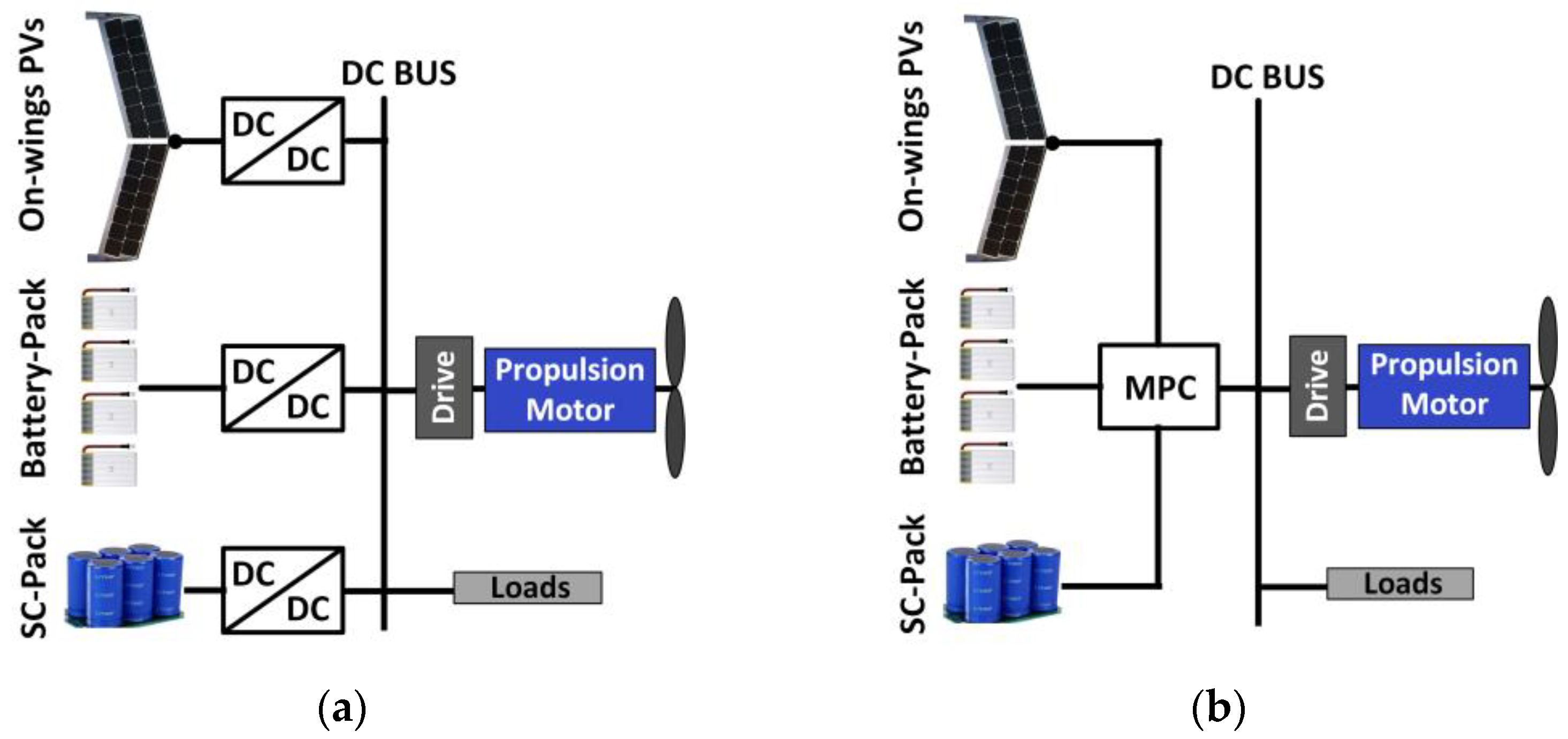
:1. Introduction
- (1)
- Fully controlled voltage step-down and step-up capability for the battery and SC was obtained at no extra cost/component size;
- (2)
- A significantly wider voltage range was available for the SC to maximize the utilization of its energy capacity and hence reduce its size without added penalties in terms of components count, current stress, and the sizes of the corresponding inductors;
- (3)
- The ability to reduce the switching current ripple in inductors by using the interleaved phase-shifted carriers modulation technique for the different input port currents.
2. The Proposed Converter Topology
3. Operation of the Proposed Converter
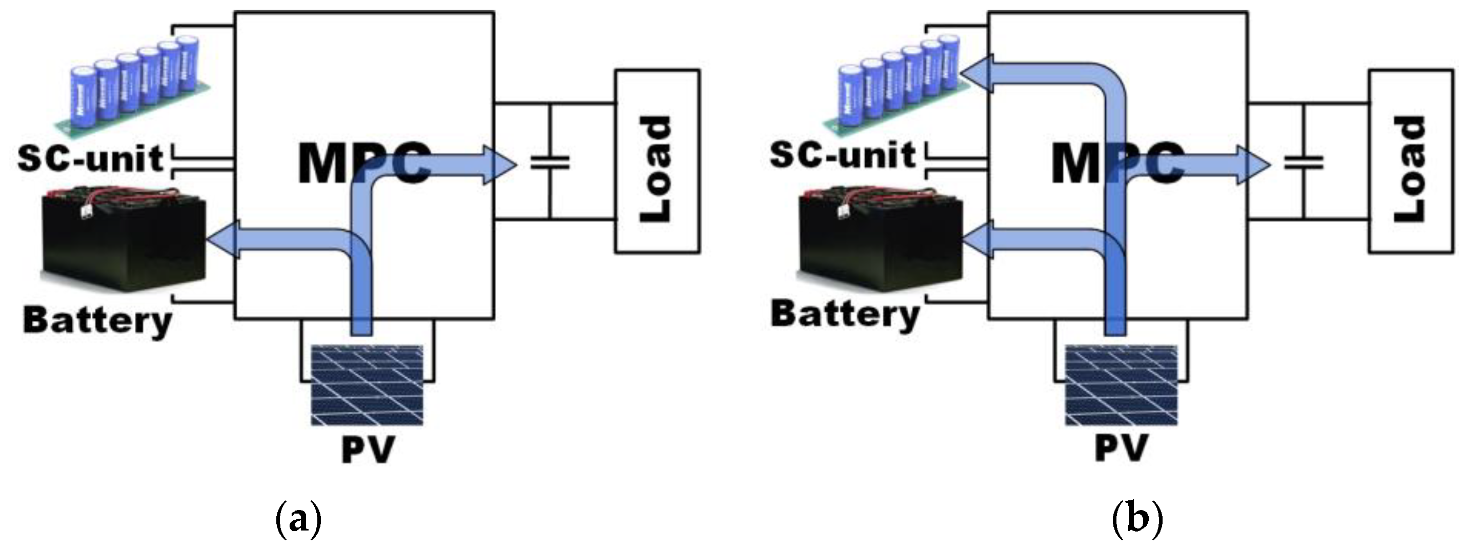
- Single input–double output (SIDO) mode (Figure 3a): where the PV supplies the required load power whilst any excess is charging the battery;
- Single input–triple output (SITO) mode (Figure 3b): where a significant amount of power is produced by the PV that can supply the load power, and due to limitations of maximum charging power of the battery, all excess is stored in the SC;
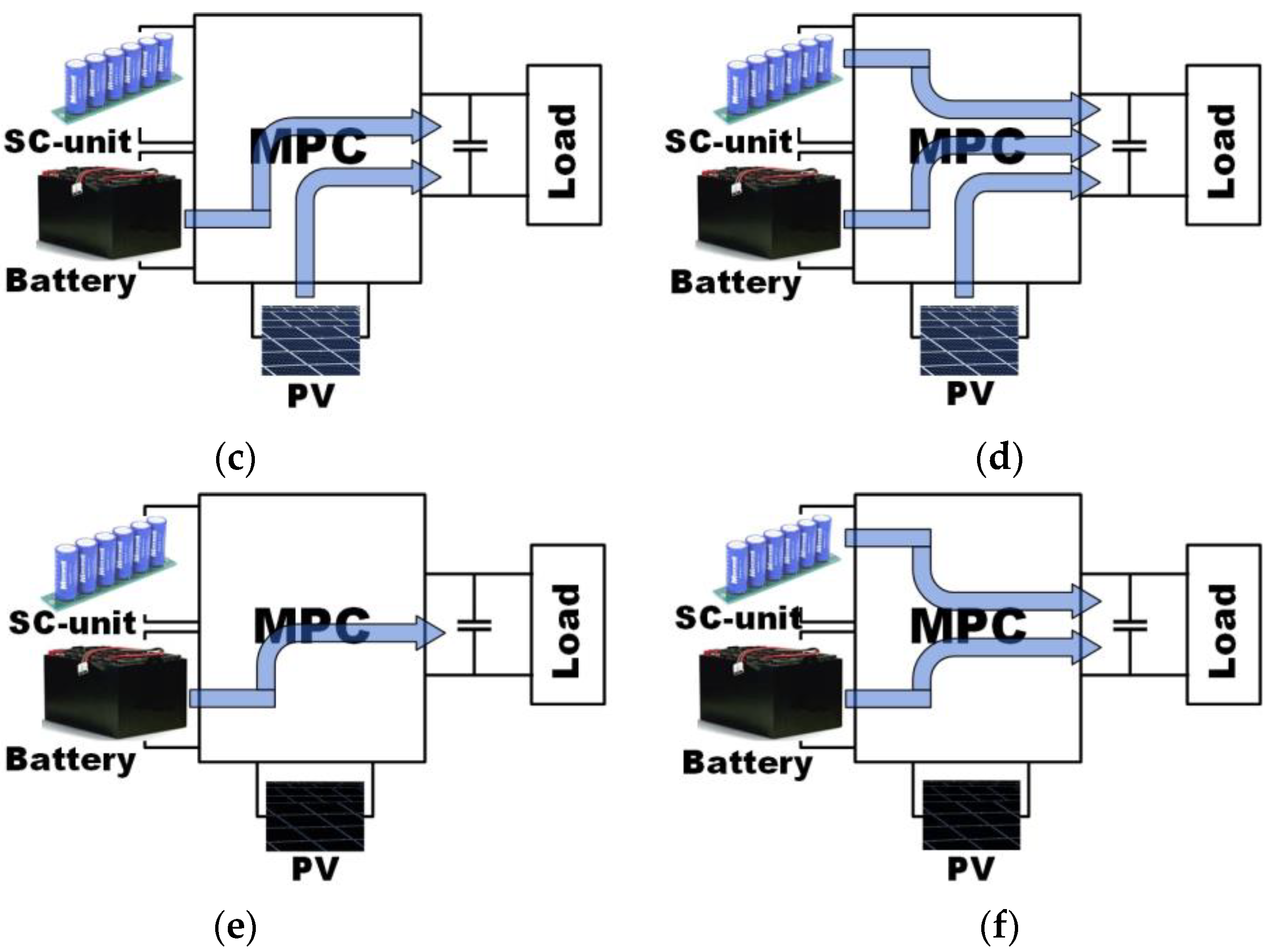
- Double input–single output mode-I (DISO-I) (Figure 3c): where the PV is unable to supply the load power, and any deficit is provided by the battery, where the load is not excessive (medium power peaks);
- Triple input–single output (TISO) mode (Figure 3d): where the PV, the battery, and the SC are supplying the load power during high power peaks, which exceed the available PV power and the battery discharge power capability;
- Single input–single output (SISO) mode (Figure 3e): where the battery provides power for supplying the load during the unavailability of the PV power;
- Double input–single output mode-II (DISO-II) (Figure 3f): where both the battery and the SC provide power for supplying the load during significant load power peaks that happen during the unavailability of PV power.
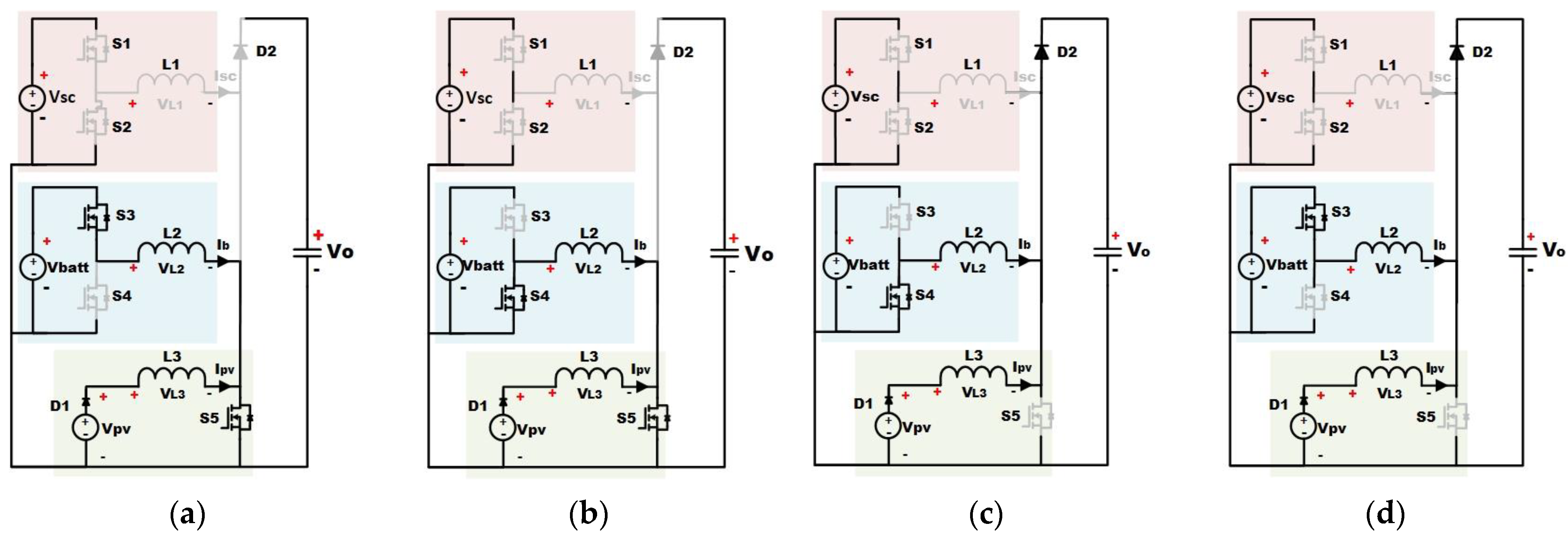
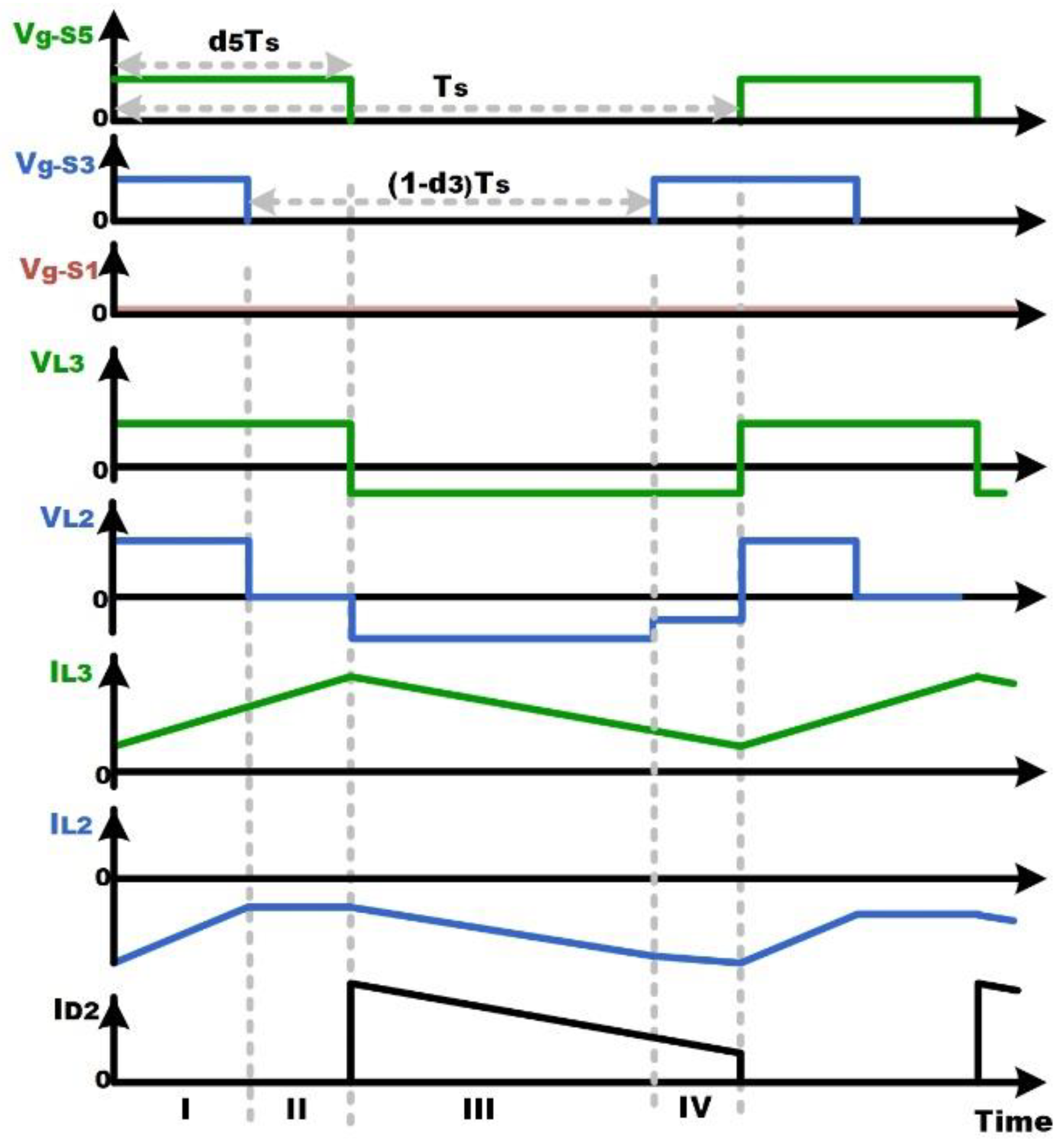
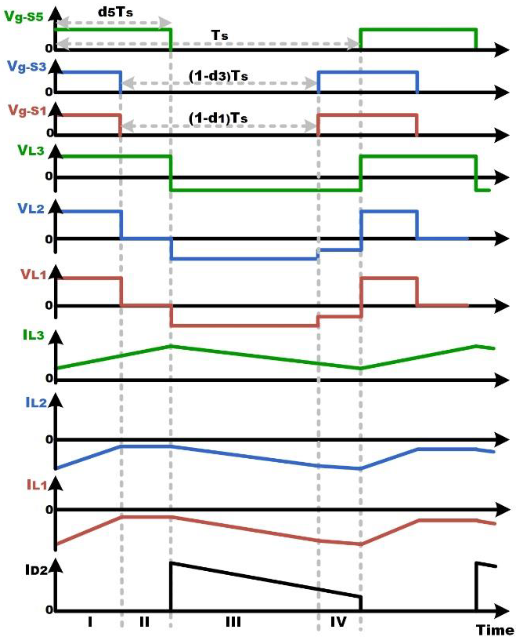
3.1. Operation Principle during the SIDO Mode
- Step I: PV switch S5 is turned ON whilst the battery stage switch S3 is still in conduction from the previous cycle. The voltage across L3 is VPV, and the voltage across L2 is Vbatt, where the diode D2 is OFF;
- Step II: S5 is still in conduction, and D2 is still OFF when S3 is switched OFF. The voltage across the L2 becomes zero (shorted to ground via S4 and S5) whilst the voltage across L3 is still VPV;
- Step III: S5 is switched OFF, and D2 starts conduction whilst S3 is still OFF. Therefore, the voltage across the L2 is (-VO), and the voltage across L3 is (VPV-VO);
- Step IV: S5 is still OFF, and D2 is still ON when S3 is switched ON. Therefore, the voltage across the L2 is (Vbatt-VO), and the voltage across L3 is (VPV-VO).
3.2. Operation Principle during the SITO Mode
3.3. Operation Principle during the DISO-I and TISO Modes
3.4. Operation Principle of the SISO Modes
3.5. Operation Principle during the DISO-II Modes
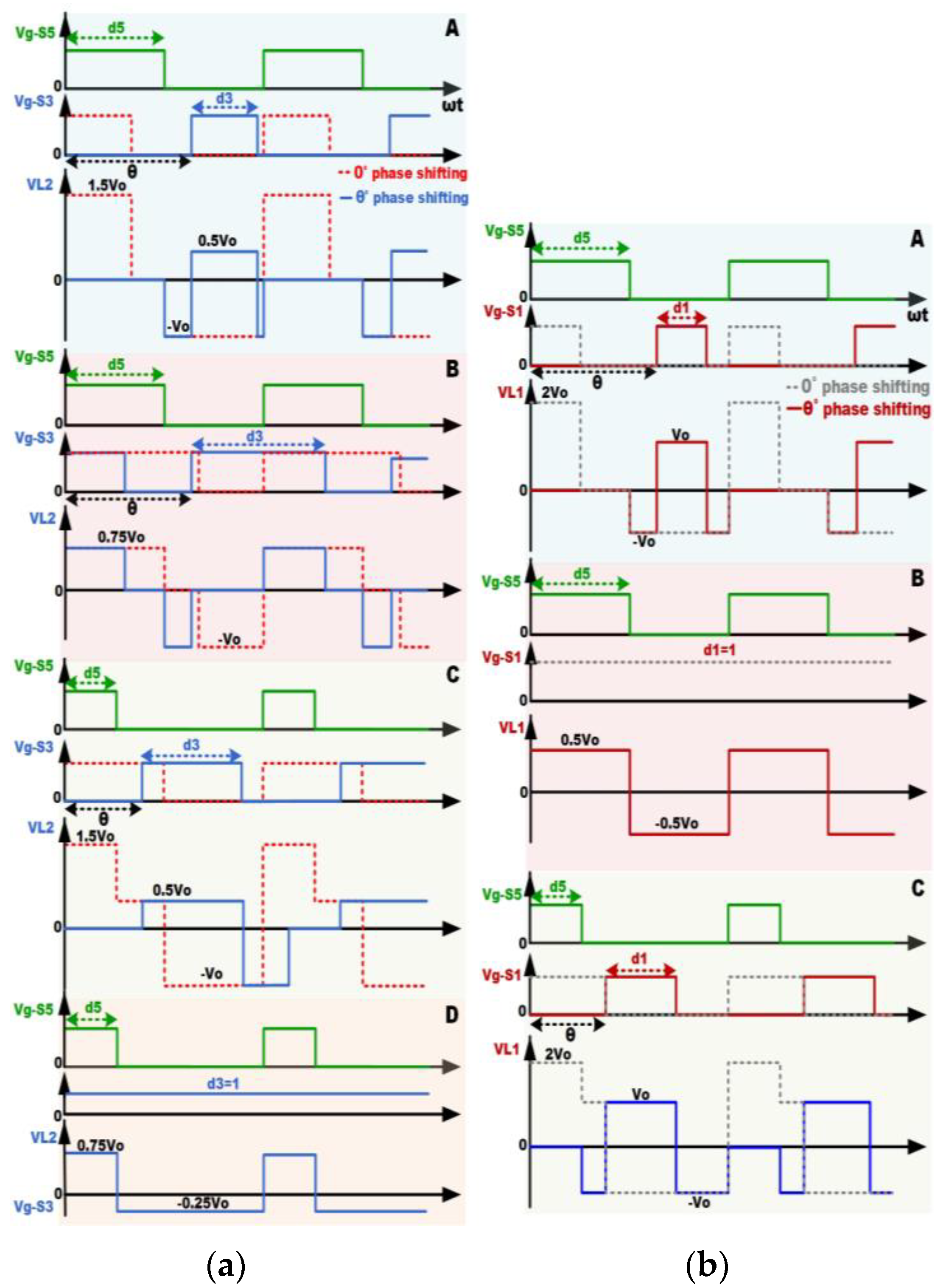
4. The Phase-Shifted Carriers Modulation
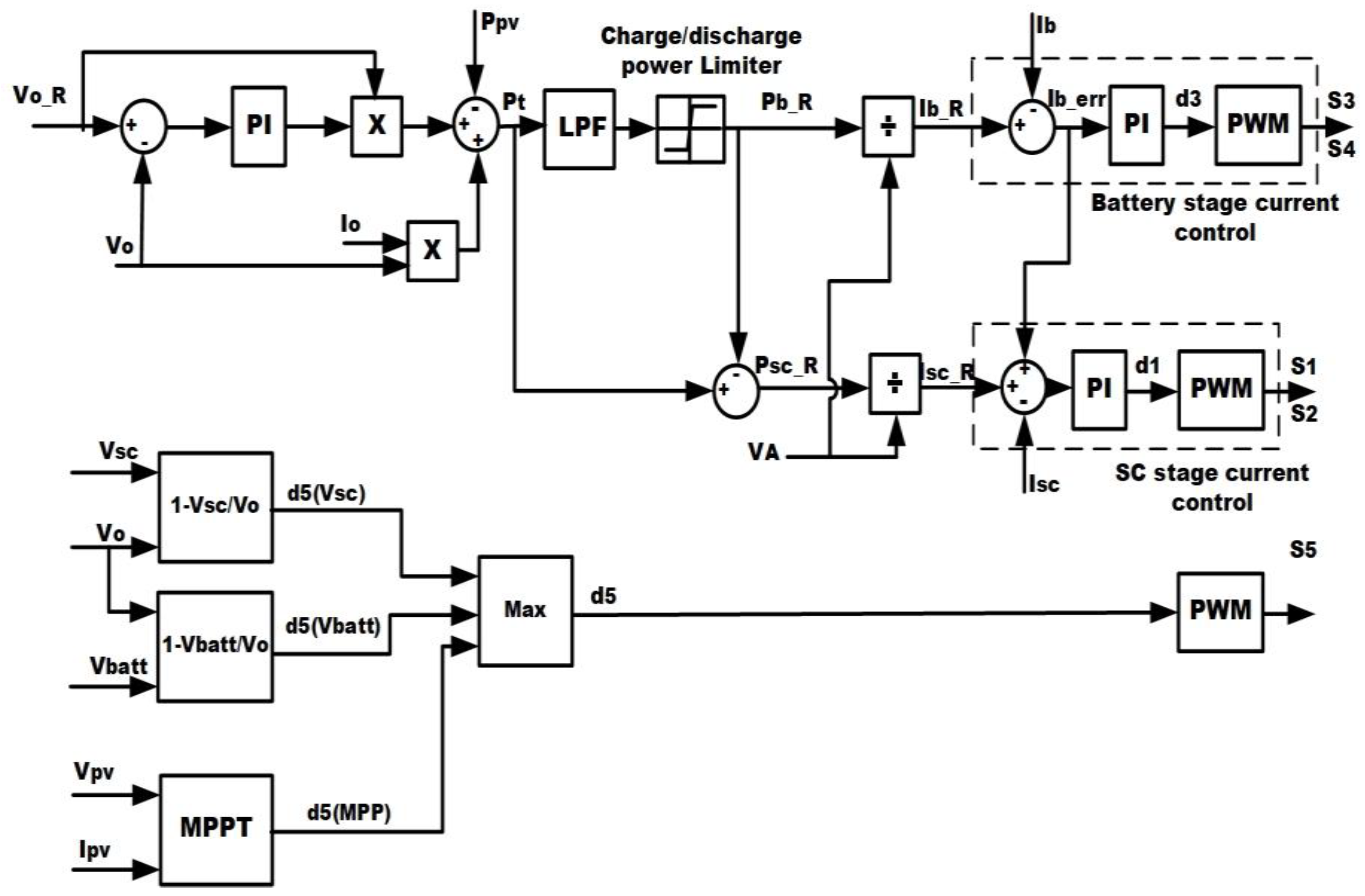
5. Control of the Proposed Converter
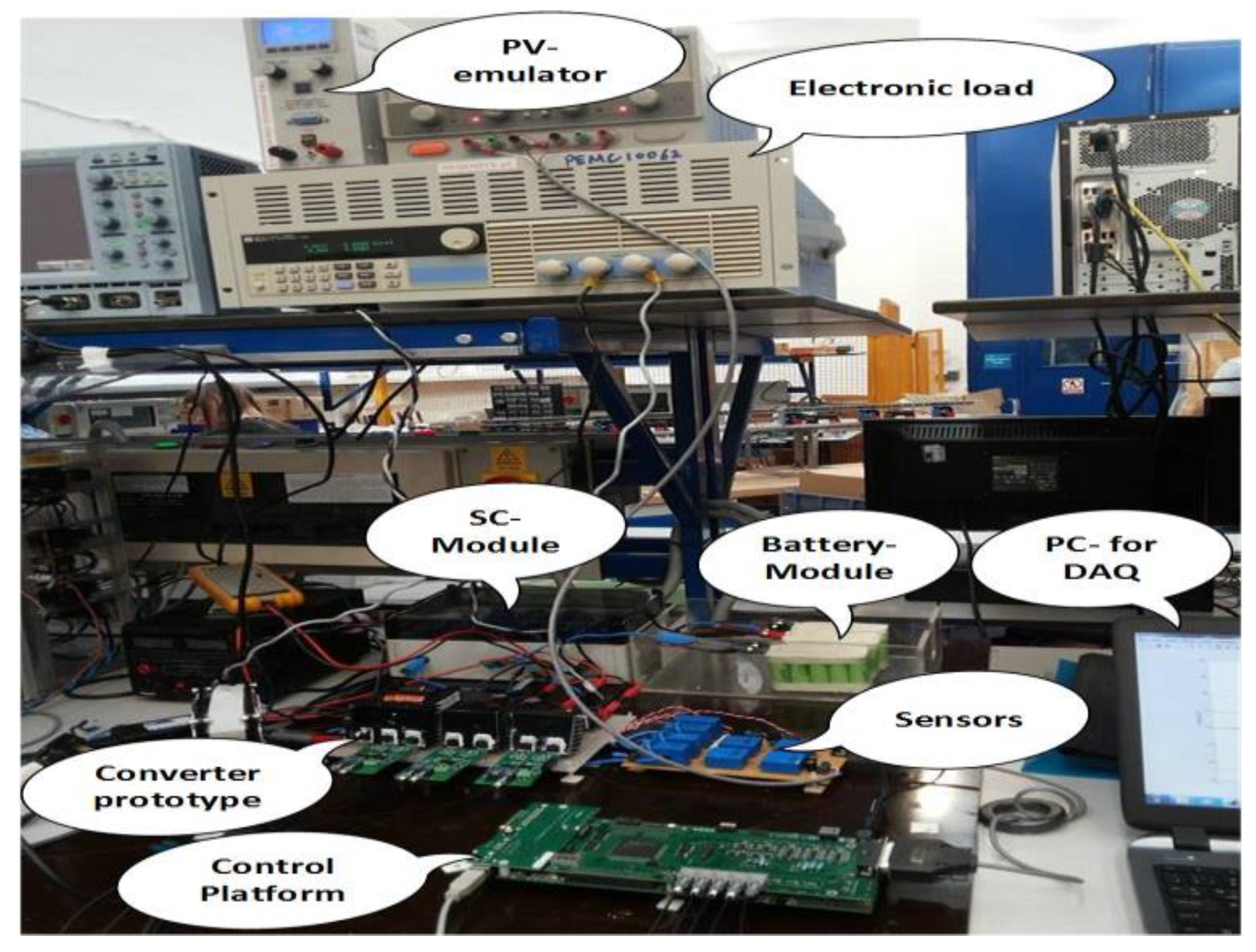
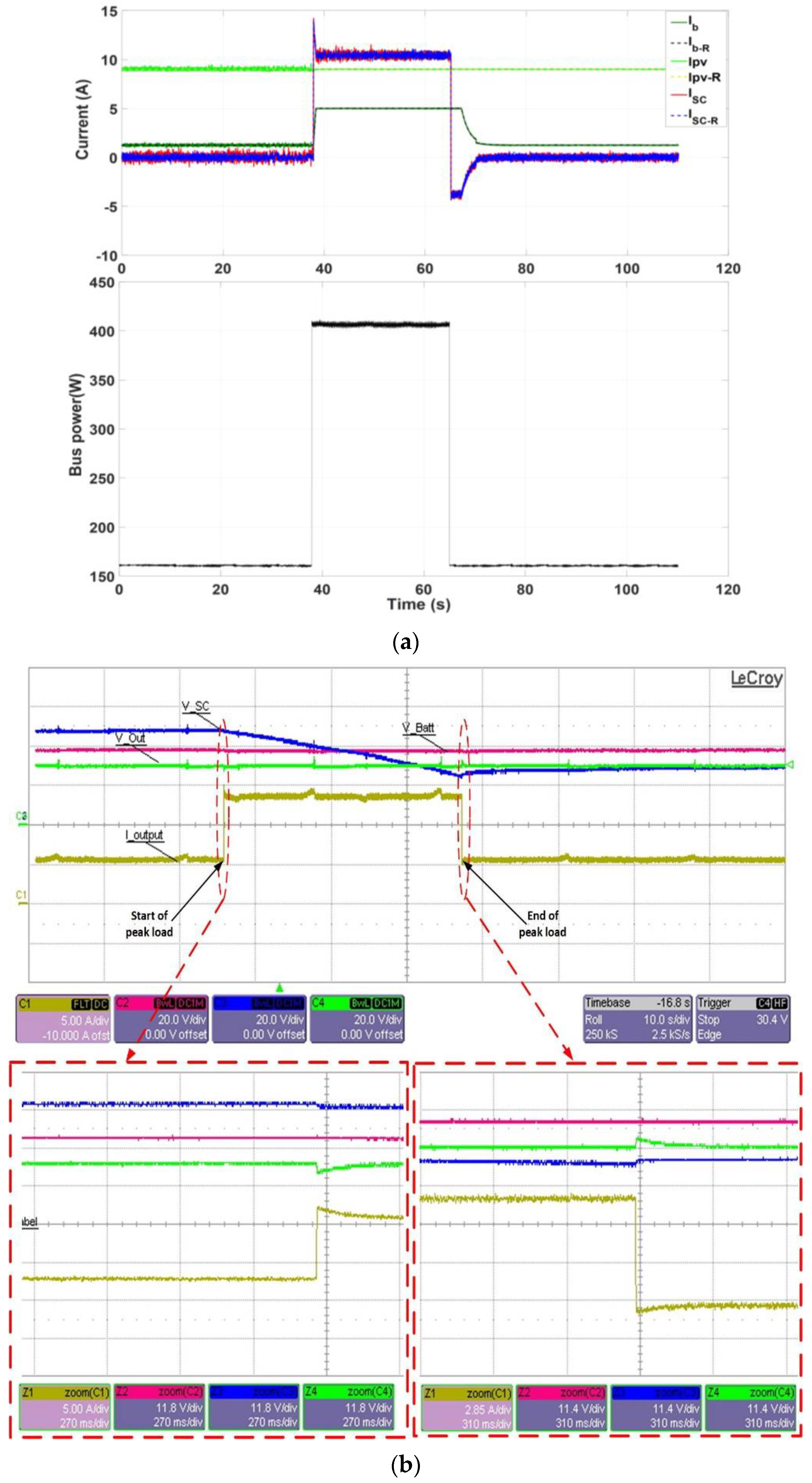
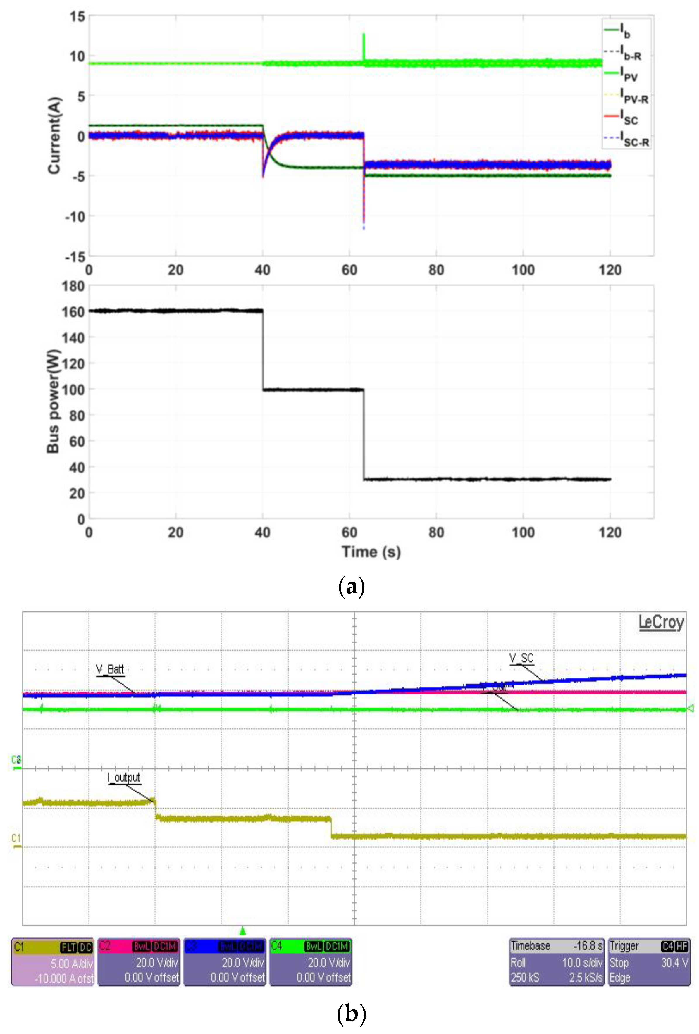
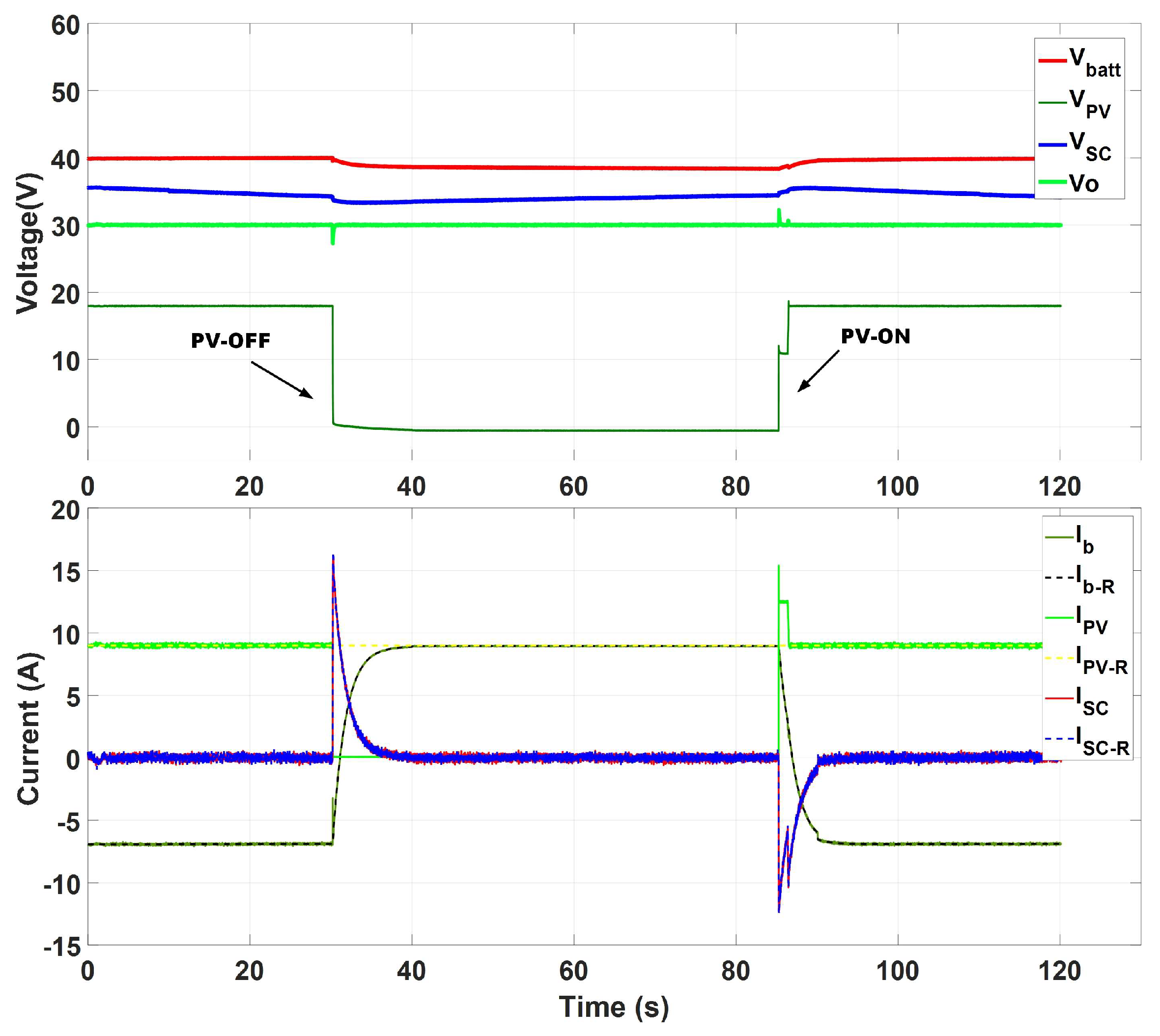
6. Experimental Results
7. Conclusions
Author Contributions
Funding
Institutional Review Board Statement
Informed Consent Statement
Data Availability Statement
Acknowledgments
Conflicts of Interest
References
- Zeng, Y.; Zhang, R.; Lim, T.J. Wireless communications with unmanned aerial vehicles: Opportunities and challenges. IEEE Commun. Mag. 2016, 54, 36–42. [Google Scholar] [CrossRef] [Green Version]
- Yanmaz, E.; Yahyanejad, S.; Rinner, B.; Hellwagner, H.; Bettstetter, C. Drone networks: Communications, coordination, and sensing. Ad Hoc Netw. 2018, 68, 1–15. [Google Scholar] [CrossRef]
- Shakhatreh, H.; Sawalmeh, A.H.; Al-Fuqaha, A.; Dou, Z.; Almaita, E.; Khalil, I.; Othman, N.S.; Khreishah, A.; Guizani, M. Unmanned Aerial Vehicles (UAVs): A Survey on Civil Applications and Key Research Challenges. IEEE Access 2019, 7, 48572–48634. [Google Scholar] [CrossRef]
- Boukoberine, M.N.; Zhou, Z.; Benbouzid, M. A critical review on unmanned aerial vehicles power supply and energy management: Solutions, strategies, and prospects. Appl. Energy 2019, 255, 113823. [Google Scholar] [CrossRef]
- D’Sa, R.; Henderson, T.; Jenson, D.; Calvert, M.; Heller, T.; Schulz, B.; Kilian, J.; Papanikolopoulos, N. Design and experiments for a transformable solar-UAV. In Proceedings of the 2017 IEEE International Conference on Robotics and Automation (ICRA), Singapore, 29 May–3 June 2017. [Google Scholar]
- Padilla, G.E.G.; Kim, K.-J.; Park, S.-H.; Yu, K.-H. Flight Path Planning of Solar-Powered UAV for Sustainable Communication Relay. IEEE Robot. Autom. Lett. 2020, 5, 6772–6779. [Google Scholar] [CrossRef]
- Dwivedi, V.S.; Giri, D.K.; Ghosh, A.K.; Kamath, G.M. Optimal Energy Utilization for a Solar-Powered Aircraft Using Sliding-Mode-Based Attitude Control. IEEE Trans. Aerosp. Electron. Syst. 2021, 57, 105–118. [Google Scholar] [CrossRef]
- Tang, S.; Zhang, L.; Guo, P.; Liu, G.; Zhang, Y.; Li, Q.; Gu, Y.; Lin, C. Processing of Monostatic SAR Data With General Configurations. IEEE Trans. Geosci. Remote Sens. 2015, 53, 6529–6546. [Google Scholar] [CrossRef]
- Xu, W.; Wang, B.; Xiang, M.; Wang, S.; Jianfeng, Y. A Novel Motion Compensation Approach Based on Symmetric Triangle Wave Interferometry for UAV SAR Imagery. IEEE Access 2020, 8, 104996–105007. [Google Scholar] [CrossRef]
- Gong, A.; MacNeill, R.; Verstraete, D.; Palmer, J.L. Analysis of a Fuel-Cell/Battery/Supercapacitor Hybrid Propulsion System for a UAV Using a Hardware-in-the-Loop Flight Simulator. In Proceedings of the 2018 AIAA/IEEE Electric Aircraft Technologies Symposium (EATS), Cincinnati, OH, USA, 12–14 July 2018. [Google Scholar]
- Zhang, X.; Liu, L.; Dai, Y.; Lu, T. Experimental investigation on the online fuzzy energy management of hybrid fuel cell/battery power system for UAVs. Int. J. Hydrogen Energy 2018, 43, 10094–10103. [Google Scholar] [CrossRef]
- Boukoberine, M.N.; Zhou, Z.; Benbouzid, M.; Donateo, T. A Frequency Separation Rule-based Power Management Strategy for a Hybrid Fuel Cell-Powered Drone. In Proceedings of the IECON 2020 the 46th Annual Conference of the IEEE Industrial Electronics Society, Singapore, 19–21 October 2020. [Google Scholar]
- Lee, B.; Kwon, S.; Park, P.; Kim, K. Active power management system for an unmanned aerial vehicle powered by solar cells, a fuel cell, and batteries. IEEE Trans. Aerosp. Electron. Syst. 2014, 50, 3167–3177. [Google Scholar] [CrossRef]
- Fares, A.; Klumpner, C.; Rashed, M. Design Considerations to Optimise Supercapacitor-based Energy Storage Systems for Aerospace Applications. In Proceedings of the 2018 IEEE International Conference on Electrical Systems for Aircraft, Railway, Ship Propulsion and Road Vehicles & International Transportation Electrification Conference (ESARS-ITEC), Nottingham, UK, 7–9 November 2018. [Google Scholar]
- Fares, A.M.; Kippke, M.; Rashed, M.; Klumpner, C.; Bozhko, S. Development of a Smart Supercapacitor Energy Storage System for Aircraft Electric Power Systems. Energies 2021, 14, 8056. [Google Scholar] [CrossRef]
- Zhang, Y.; Gao, Y.; Zhou, L.; Sumner, M. A Switched-Capacitor Bidirectional DC–DC Converter With Wide Voltage Gain Range for Electric Vehicles With Hybrid Energy Sources. IEEE Trans. Power Electron. 2018, 33, 9459–9469. [Google Scholar] [CrossRef]
- Zhang, Y.; Liu, Q.; Gao, Y.; Li, J.; Sumner, M. Hybrid Switched-Capacitor/Switched-Quasi-Z-Source Bidirectional DC–DC Converter With a Wide Voltage Gain Range for Hybrid Energy Sources EVs. IEEE Trans. Ind. Electron. 2019, 66, 2680–2690. [Google Scholar] [CrossRef]
- Elsayad, N.; Moradisizkoohi, H.; Mohammed, O.A. A New Hybrid Structure of a Bidirectional DC-DC Converter With High Conversion Ratios for Electric Vehicles. IEEE Trans. Veh. Technol. 2020, 69, 194–206. [Google Scholar] [CrossRef]
- Pires, V.F.; Foito, D.; Cordeiro, A. A DC–DC Converter With Quadratic Gain and Bidirectional Capability for Batteries/Supercapacitors. IEEE Trans. Ind. Appl. 2018, 54, 274–285. [Google Scholar] [CrossRef]
- Aharon, I.; Kuperman, A.; Shmilovitz, D. Analysis of Dual-Carrier Modulator for Bidirectional Noninverting Buck–Boost Converter. IEEE Trans. Power Electron. 2015, 30, 840–848. [Google Scholar] [CrossRef]
- Khan, M.A.; Ahmed, A.; Husain, I.; Sozer, Y.; O Badawy, M. Performance Analysis of Bidirectional DC–DC Converters for Electric Vehicles. IEEE Trans. Ind. Appl. 2015, 51, 3442–3452. [Google Scholar] [CrossRef]
- Khan, M.A.; Husain, I.; Sozer, Y. A Bidirectional DC–DC Converter With Overlapping Input and Output Voltage Ranges and Vehicle to Grid Energy Transfer Capability. IEEE J. Emerg. Sel. Top. Power Electron. 2014, 2, 507–516. [Google Scholar] [CrossRef]
- Elsayad, N.; Moradisizkoohi, H.; Mohammed, O.A. Design and Implementation of a New Transformerless Bidirectional DC–DC Converter With Wide Conversion Ratios. IEEE Trans. Ind. Electron. 2019, 66, 7067–7077. [Google Scholar] [CrossRef]
- Wu, H.; Zhang, J.; Xing, Y. A Family of Multiport Buck–Boost Converters Based on DC-Link-Inductors (DLIs). IEEE Trans. Power Electron. 2015, 30, 735–746. [Google Scholar] [CrossRef]
- Wu, H.; Chen, R.; Zhang, J.; Xing, Y.; Hu, H.; Ge, H. A Family of Three-Port Half-Bridge Converters for a Stand-Alone Renewable Power System. IEEE Trans. Power Electron. 2011, 26, 2697–2706. [Google Scholar] [CrossRef]
- Solero, L.; Lidozzi, A.; Pomilio, J.A. Design of multiple-input power converter for hybrid vehicles. IEEE Trans. Power Electron. 2005, 20, 1007–1016. [Google Scholar] [CrossRef]
- Sikkabut, S.; Mungporn, P.; Ekkaravarodome, C.; Bizon, N.; Tricoli, P.; Nahid-Mobarakeh, B.; Pierfederici, S.; Davat, B.; Thounthong, P. Control of High-Energy High-Power Densities Storage Devices by Li-ion Battery and Supercapacitor for Fuel Cell/Photovoltaic Hybrid Power Plant for Autonomous System Applications. IEEE Trans. Ind. Appl. 2016, 52, 4395–4407. [Google Scholar] [CrossRef] [Green Version]
- Xu, Q.; Xiao, J.; Hu, X.; Wang, P.; Lee, M.Y. A Decentralized Power Management Strategy for Hybrid Energy Storage System With Autonomous Bus Voltage Restoration and State-of-Charge Recovery. IEEE Trans. Ind. Electron. 2017, 64, 7098–7108. [Google Scholar] [CrossRef]
- Mesbahi, T.; Rizoug, N.; Khenfri, F.; Bartholomeüs, P.; Le Moigne, P. Dynamical modelling and emulation of Li-ion batteries-supercapacitors hybrid power supply for electric vehicle applications. IET Electr. Syst. Transp. 2017, 7, 161–169. [Google Scholar] [CrossRef]
- Torreglosa, J.P.; Garcia, P.; Fernández, L.M.; Jurado, F. Predictive Control for the Energy Management of a Fuel-Cell–Battery–Supercapacitor Tramway. IEEE Trans. Ind. Inform. 2014, 10, 276–285. [Google Scholar] [CrossRef]
- Camara, M.B.; Gualous, H.; Gustin, F.; Berthon, A. Design and New Control of DC/DC Converters to Share Energy Between Supercapacitors and Batteries in Hybrid Vehicles. IEEE Trans. Veh. Technol. 2008, 57, 2721–2735. [Google Scholar] [CrossRef]
- Wai, R.-J.; Chen, B.-H. High-Efficiency Dual-Input Interleaved DC–DC Converter for Reversible Power Sources. IEEE Trans. Power Electron. 2014, 29, 2903–2921. [Google Scholar] [CrossRef]
- Hintz, A.; Prasanna, U.R.; Rajashekara, K. Novel Modular Multiple-Input Bidirectional DC–DC Power Converter (MIPC) for HEV/FCV Application. IEEE Trans. Ind. Electron. 2015, 62, 3163–3172. [Google Scholar] [CrossRef]
- Lai, C.-M.; Cheng, Y.-H.; Hsieh, M.-H.; Lin, Y.-C. Development of a Bidirectional DC/DC Converter With Dual-Battery Energy Storage for Hybrid Electric Vehicle System. IEEE Trans. Veh. Technol. 2017, 67, 1036–1052. [Google Scholar] [CrossRef]
- Fares, A.M.; Klumpner, C.; Sumner, M. A Novel Modular Multiport Converter for Enhancing the Performance of Photovoltaic-Battery Based Power Systems. Appl. Sci. 2019, 9, 3948. [Google Scholar] [CrossRef] [Green Version]
- Sathishkumar, R.; Kollimalla, S.K.; Mishra, M.K. Dynamic energy management of micro grids using battery super capacitor combined storage. In Proceedings of the 2012 Annual IEEE India Conference (INDICON), Kochi, India, 7–9 December 2012. [Google Scholar]
- Zhou, H.; Bhattacharya, T.; Tran, D.; Siew, T.S.T.; Khambadkone, A. Composite Energy Storage System Involving Battery and Ultracapacitor With Dynamic Energy Management in Microgrid Applications. IEEE Trans. Power Electron. 2011, 26, 923–930. [Google Scholar] [CrossRef]
- Kollimalla, S.K.; Mishra, M.K.; Narasamma, N.L. Design and Analysis of Novel Control Strategy for Battery and Supercapacitor Storage System. IEEE Trans. Sustain. Energy 2014, 5, 1137–1144. [Google Scholar] [CrossRef]


| Parameters | Standard Boost Converter | Boost Converter in [17] | Boost Converter in [18] | Buck/Boost Converter in [20] | Buck/Boost Converter in [23] | SC-Stage in the Proposed MPC |
|---|---|---|---|---|---|---|
| Range of SC voltage swing required | Vmin = 0.25 Vo Vmax = Vo | Vmin = 0.09 Vo Vmax = 0.35 Vo | Vmin = 0.08 Vo Vmax = 0.3 Vo | Vmin = 0.5 Vo Vmax = 2 Vo | Vmin = 0.5 Vo Vmax = 2 Vo | Vmin = 0.5 Vo Vmax = 2 Vo |
| Duty cycle at Vmin | 0.75 | 0.75 | 0.55 | 0.5 | 0.5 | 0.5 |
| Count of simiconductor switches | 2 | 5 | 6 | 4 | 3 | 2 |
| Count of inductors | 1 | 2 | 2 | 1 | 2 | 1 |
| Count of capacitors * | 0 | 4 | 4 | 0 | 2 | 0 |
| Inductor max. current | 4 Io | IL1 = 11.5 Io IL2 = 4 Io | IL1 = 7.7 Io IL2 = 4.4 Io | 2 Io | IL1 = 3 Io IL2 = Io | 2 Io |
| Inductor’s inductance | ||||||
| Max. voltage stress on semiconductor switches | Vo | 0.3 Vo | Q1,5 = 0.2 Vo Q2 = 0.4 Vo Q3,4,6 = 0.6 Vo | 2 Vo | 2.5 Vo | 2 Vo |
| Max. current stress on semiconductor switches | Q1,2 ≥ 4 Io | Q1 ≥ 13 Io Q2,3,5 ≥ 4 Io Q4≥ 5 Io | Q1 ≥ 12 Io Q2,5 ≥ 6 Io Q3,4,6≥ 2 Io | Q1,2 ≥ 2 Io | Q1 ≥ 4 Io Q2,3 ≥ 2 Io | Q1,2 ≥ 2 Io Q1,2≥ Io + Ipv + Ibatt |
| Vbatt | 1.5 Vo | 0.75 Vo | |||
|---|---|---|---|---|---|
| VPV | |||||
| 0.5 Vo | d3 ≈ 0.33 d5 = 0.5 | A | d3 ≈ 0.67 d5 = 0.5 | B | |
| 0.75 Vo | d3 = 0.5 d5 = 0.25 | C | d3 = 1 d5 = 0.25 | D | |
| VSC | 2 Vo | 0.5 Vo | |||
|---|---|---|---|---|---|
| Vpv | |||||
| 0.5 Vo | d1 ≈ 0.25 d5 = 0.5 | A | d1 ≈ 1 d5 = 0.5 | B | |
| 0.75 Vo | d1 = 0.375 d5 = 0.25 | C | |||
| Type/Name | Rating/Specifications |
|---|---|
| Battery module | 42 V/6 Ah based on Panasonic NCR18650B cell with Vmax = 42 V and Vmin = 25 V |
| SC-module | 8 F/60 V based on AVX SCCW45B107 cell with Vmax = 60 V and Vmin = 15 V |
| PV module emulator | VpvMPP = (15 − 22.5) V, IpvMPP = (6 − 9) A |
| SC stage inductor (L1) | 120 μH |
| Battery stage inductor (L2) | 240 μH |
| PV module inductor (L3) | 120 μH |
| DC-link capacitor (CO) | 2200 μF |
| Switching frequency (Fs) | 10 kHz |
Publisher’s Note: MDPI stays neutral with regard to jurisdictional claims in published maps and institutional affiliations. |
© 2022 by the authors. Licensee MDPI, Basel, Switzerland. This article is an open access article distributed under the terms and conditions of the Creative Commons Attribution (CC BY) license (https://creativecommons.org/licenses/by/4.0/).
Share and Cite
Fares, A.M.; Klumpner, C.; Sumner, M. A Novel Multiport DC-DC Converter for Enhancing the Design and Performance of Battery–Supercapacitor Hybrid Energy Storage Systems for Unmanned Aerial Vehicles. Appl. Sci. 2022, 12, 2767. https://doi.org/10.3390/app12062767
Fares AM, Klumpner C, Sumner M. A Novel Multiport DC-DC Converter for Enhancing the Design and Performance of Battery–Supercapacitor Hybrid Energy Storage Systems for Unmanned Aerial Vehicles. Applied Sciences. 2022; 12(6):2767. https://doi.org/10.3390/app12062767
Chicago/Turabian StyleFares, Ahmed M., Christian Klumpner, and Mark Sumner. 2022. "A Novel Multiport DC-DC Converter for Enhancing the Design and Performance of Battery–Supercapacitor Hybrid Energy Storage Systems for Unmanned Aerial Vehicles" Applied Sciences 12, no. 6: 2767. https://doi.org/10.3390/app12062767