Article

Dual Band Electrically Small Complementary Double Negative Structure Loaded Metamaterial Inspired Circular Microstrip Patch Antenna for WLAN Applications

School of Engineering, Cochin University of Science and Technology, Kochi 682022, Kerala, India
*
Author to whom correspondence should be addressed.
Appl. Sci. 2022, 12(6), 3035; https://doi.org/10.3390/app12063035
Submission received: 29 December 2021 / Revised: 12 February 2022 / Accepted: 17 February 2022 / Published: 16 March 2022
(This article belongs to the Special Issue Nature-Inspired Mechanical Metamaterials)

Abstract

:
In this article, a compact dual band metamaterial inspired circular microstrip patch antenna for WLAN applications is presented. The antenna consists of a circular patch loaded with a complementary double negative metamaterial structure which produces a percentage miniaturisation of 60.7%. The circular microstrip patch antenna used for developing the proposed antenna has a resonant frequency of 6.2 GHz with an impedance bandwidth of 3.5% before the metamaterial structure is applied upon it. The loading of the proposed metamaterial structure inspires the antenna to lower its resonant frequency with enhanced bandwidth and generate one additional resonance. The designed antenna can be tuned throughout the C-band by simply altering the size of the metamaterial structure loaded upon it. However, the prototype of the antenna is designed for the most commonly used wireless communication bands at 2.4 GHz and 5.2 GHz. The 10 dB impedance bandwidth of 1.63% at 2.4 GHz and 13.15% at 5.2 GHz are achieved by this design. The electrical parameters of the proposed antenna are ka = 0.72 and QChu = 4.07 rendering it electrically small. This electrical compactness and bandwidth enhancement are caused by the loading of metamaterial structure. The proposed antenna is fabricated on low cost FR4 substrate and has an overall compact electrical size of 0.164 λ0 × 0.164 λ0 × 0.013 λ0 and physical dimensions 20 × 20 × 1.6 mm3, with peak gain 3.8 dBi and 2.9 dBi at 2.4 GHz and 5.2 GHz respectively.

1. Introduction

The communication industry today requires miniaturised, compact antennas with enhanced bandwidth for developing smaller and high-speed communication systems. Miniaturisation of antennas can be achieved by converting conventional antenna designs into electrically small antennas (ESAs). One of the most commonly used conventional types of antenna is microstrip patches because of their advantages such as ease of fabrication, simple design, low cost, etc. However, they have radiating patch size much larger than the dimensions required for components that can be accommodated in modern compact devices. This paper focuses on the conversion of a conventional circular patch into an electrically small antenna with dual-band and enhanced bandwidth using metamaterial loading.
ESAs are antennas having certain defining electrical parameters proposed by Chu and then by Wheeler [1]. These parameters are derived mathematically from wave number ‘k’ = 2π0 and spherical radius around the highest dimension of the unit cell ‘a’. Based on these values ESAs are defined using the mathematical formula ka < 1. Antenna designers find attractive features of ESAs—such as compactness of size, simplicity of structure, etc.—useful for developing compact antennas for modern applications [2,3,4]. ESAs also have certain disadvantages such as high reactance and low radiation resistance due to their small electrical size which in turn results in high quality factor (Q). In ESAs decrease of the value of electrical size ‘ka’ closely correspond to the decrease of parameters such as bandwidth, efficiency, and gain [1]. Use of defected ground structures [5,6] and metamaterials (MTMs) [7,8] are the two most commonly used methods for developing ESAs from conventional antennas.
MTMs are practically developed by Smith et al. [9], and their unique properties attract antenna designers, who incorporate them in existing antennas for performance enhancement [10,11]. MTMs are artificial electromagnetic structures with unusual properties and can be classified into mu-negative (MNG) MTM (µ < 0), epsilon-negative (ENG) MTM (ε < 0) [12,13], and double negative (DNG) MTM (µ < 0 and ε < 0) [12,14]. The most commonly used MNG-MTMs are split ring resonators (SRRs) whereas the complementary split-ring resonators (CSRRs) belong to ENG-MTMs [13].
Erentok and Ziolkowski developed the concept of electrically small MTM inspired antennas [15]. In this antenna, an MTM unit-cell has been placed in the vicinity of the driven element, thereby utilizing its features for enhancing the properties of the driven element. As a result, the impedance matching and overall radiation efficiency of the antenna are improved without using additional matching networks. Ziolkowski et al. used the MTM unit-cell as a parasitic element in the near-field of the driven element and it has become the dominant radiating component of the overall system at the desired resonant frequency [16].
Even though SRRs are generally used for the design of MTM inspired antennas with miniaturised size [15,16,17], CSRRs are loaded in patch antennas for their size reduction [18,19,20,21,22,23,24,25,26,27] because they can be easily integrated in the ground plane of the antenna without altering the radiating patch. Raval et al. successfully generated a metamaterial effect by etching CSRR in the ground plane of a circular microstrip patch antenna [18]. Compared with the conventional circular patch antenna, the effective footprint area of the antenna using CSRR as a defected ground plane, is reduced approximately by 64%. By introducing single complementary split ring in the ground plane, dual band resonance and miniaturisation have been achieved [19] and the antenna achieves about 70% reduction in the resonant frequency and 89% reduction in the radiating patch size when compared with the conventional microstrip antenna. The size of a conventional rectangular patch antenna is reduced by almost 24% using CSRR loading on the ground plane [20]. An array of the same CSRR unit-cell is also applied on microstrip patch array for obtaining an array size reduction of 40%. CSRRs are used as defected ground structures for patch antenna miniaturization [21,22,23,25]. Electrically small antennas are developed using CSRRs in the conventional patch antennas [24,26,27]. Another metamaterial inspired electrically small quad-band antenna has been developed using SRR [28]. Hence, loading of complementary structures in the ground plane can achieve greater size reduction compared to placement of ordinary SRRs in the vicinity of radiating patch.
This article explores the application of a complementary double negative metamaterial (CDNG-MTM) structure for miniaturisation of circular patch antenna. A single cell CDNG-MTM structure is loaded in ground plane and analysed for its various parameters such as return loss, fractional bandwidth, realised gain, and radiation pattern. The simulated results are measured and validated.

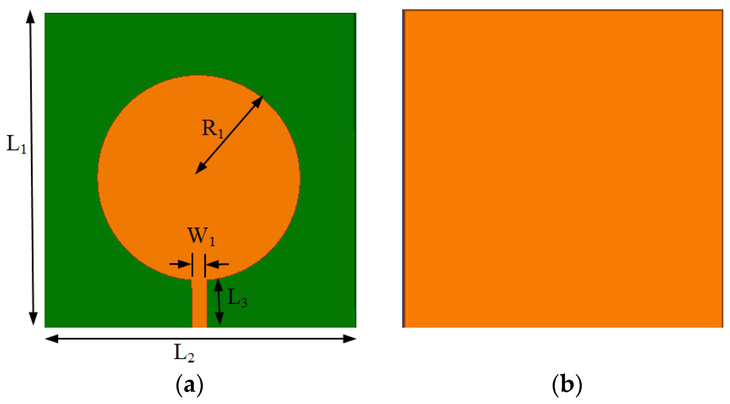
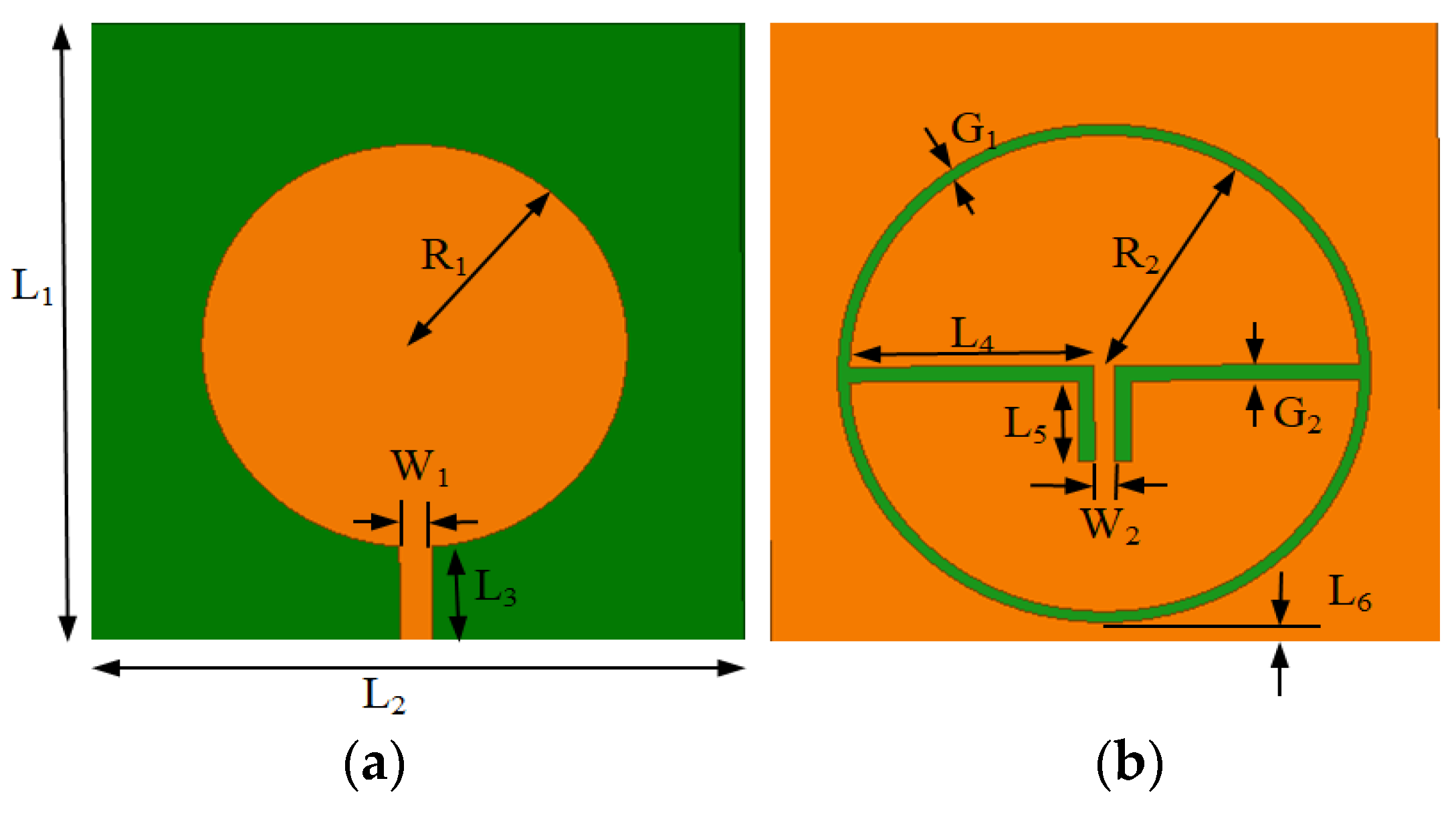
2. Circular Patch Antenna Design

The first step towards the goal of electrical size reduction of the proposed antenna is the design of a circular patch antenna operating at 6.24 GHz based on the basic patch antenna design procedure [18,29]. The initial operating frequency is chosen as 6.24 GHz because CDNG-MTM tuning would end up in final operating frequencies in WLAN application bands of 2.4 GHz and 5.2 GHz. The designed structure is shown as Figure 1. The prototype of the antenna is fabricated on an FR4 substrate. The antenna is fed with a microstrip line feed having feed-width of 1 mm and feed-length of 3.1 mm. Detailed dimensions of the circular patch antenna are given in Table 1. The simulated and measured return loss characteristics of the circular patch antenna are plotted in Figure 2.

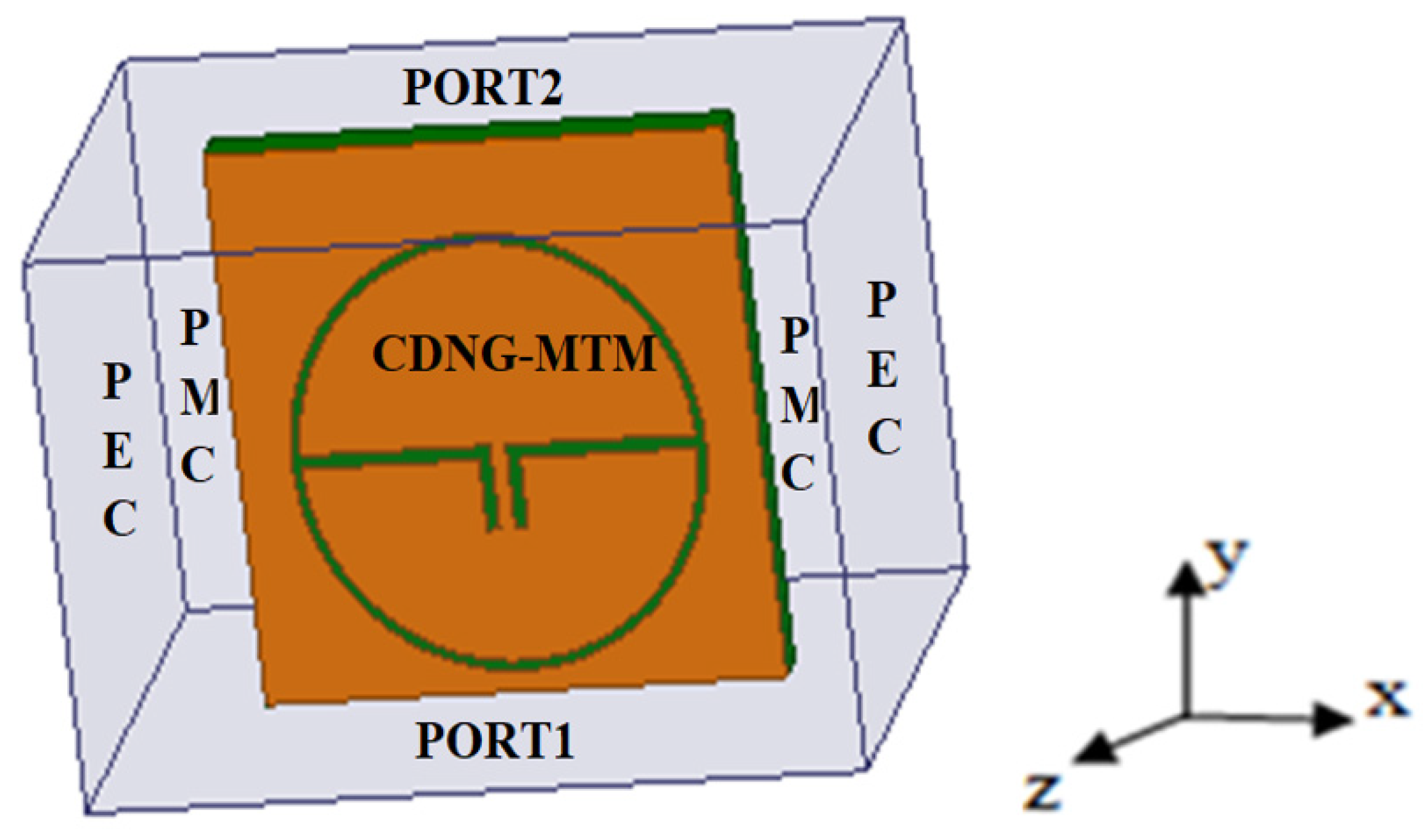
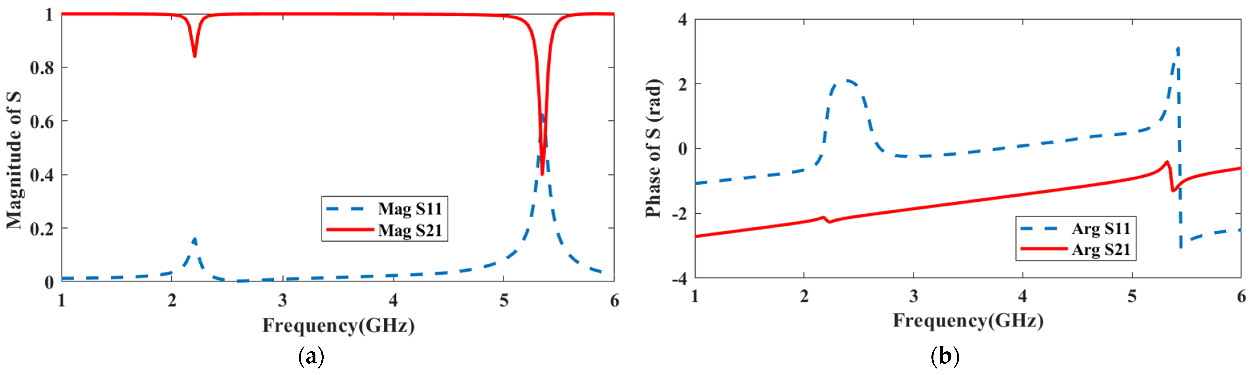
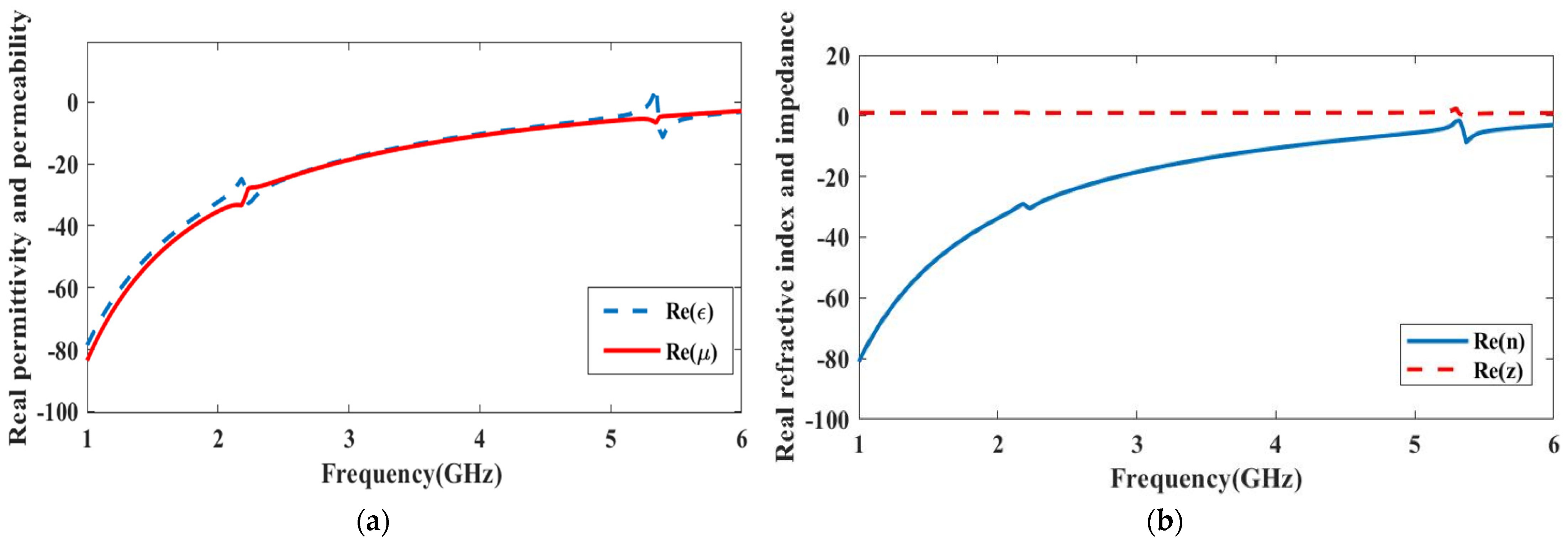
3. Design and Characterisation of CDNG-MTM

The basic DNG-MTM consists of a ring with two stub lines [30]. A modification of this basic structure is proposed by addding two extra stubs on the existing stub lines. Even though the stub length is increased by this modification, the overall size and the DNG behaviour remain unaltered. At the same time, this modification enables wider frequency tuning. Thus, the modified DNG-MTM consists of a metallic ring having two L-shaped stub lines with a gap. The distributed inductance and capacitance [31,32] effect on this ring, stub and the gap produce an LC resonator behaviour with a high-quality factor (Q). However, complementary MTM structures are more suitable for inducing MTM effect on patch antennas. On the basis of Babinet’s principle and the duality concept, a DNG-MTM has a complementary structure (CDNG-MTM) that exhibits similar operational behaviour and properties. By altering the various physical parameters—such as ring radius, stub length, etc.—tuning of the resonant frequency of the CDNG-MTM can be done. The material parameters of the CDNG-MTM can be retrieved using S-parameter retrieval method [30,33,34,35,36,37]. A two-port waveguide set up is used to extract S-parameters of the CDNG-MTM. The boundary conditions perfect magnetic conductor (PMC), perfect electric conductor (PEC) and waveguide for the extraction of S11 and S21 are shown in Figure 3. Material properties such as permittivity, permeability, refractive index, and impedance can be retrieved using S-parameters as per the following equations implemented in MATLAB™.
z = ± ( 1 + S 11 ) 2 S 21 2 ( 1 S 11 ) 2 S 21 2
e i n k 0 d = S 21 1 S 11 z 1 z + 1
n = 1 k 0 d { [ [ l n   ( e i n k 0 d )   ] + 2 m π ] i [ l n   ( e i n k 0 d )   ] }
where ‘k0’is the wavenumber in free space and ‘m’ represents branch index of refractive index, which is an integer. Relative permittivity ‘ε’ and relative permeability ‘µ’ can be calculated using the relations (4) and (5).
ε = n / z
μ = n z  
Figure 4a,b show S11 and S21 magnitude and phase plots of the CDNG structure, obtained from the waveguide setup. Figure 4a shows resonance at 2.4 GHz and 5.2 GHz, whereas, Figure 4b shows phase change at the same frequencies. Since the CDNG structure shows resonance and phase change at these frequencies, the structure exhibits metamaterial behaviour in these frequency regimes. These S-parameter values are used to extract material properties. Figure 5a,b exhibit the extracted values of relative permittivity ε, relative permeability µ, refractive index n, and impedance z. It can be observed in Figure 5a that, both permittivity and permeability show negative values over a wide range in C-band. In Figure 5b the DNG property is exhibited where n is negative. A passive material shows DNG behaviour when its n shows negative values and z shows positive values.

4. Antenna Geometry and Design

The circular patch antenna in Figure 1 is loaded with the CDNG structure on the ground plane. Loading of CDNG structure perturbs the radiating field and introduces additional capacitive and inductive effect on the basic patch antenna. This increased capacitive and inductive effect reduces the resonance frequency. Thus, the electrical size of the antenna is reduced and the ka value gets reduced to 0.72. Since the CDNG structure loaded antenna has ka < 1, it can be termed as electrically small antenna. Top and bottom view of the proposed antenna are shown in Figure 6. Design parameters of the circular patch antenna and the loaded CDNG-MTM are given in Table 1. Figure 7a,b show the current distribution of the proposed antenna at 2.43 GHz and 5.2 GHz respectively. At the lower band, current is distributed more in CDNG-MTM and less in patch and at the higher band current is distributed equally in both patch and CDNG-MTM in the ground plane. This shows that the lower band resonance is mainly due to the CDNG structure and higher band resonance is due to the combined effect of patch and CDNG-MTM. Gain plot of the proposed antenna is shown in Figure 8. It can be observed that peak gains of 3.8 dBi at 2.43 GHz and 2.9 dBi at 5.2 GHz are obtained for the proposed antenna.
In conventional antennas, miniaturisation can be achieved by increasing the substrate permittivity. Without changing the substrate material, effective permittivity can be increased by incorporating an MTM or an MTM effect within the antenna design. This in turn would reduce the size of the antenna. Thus, MTMs can function as a material substitute in achieving miniaturisation of antennas. In the proposed design also the change of effective permittivity using MTM is utilised for achieving miniaturisation.

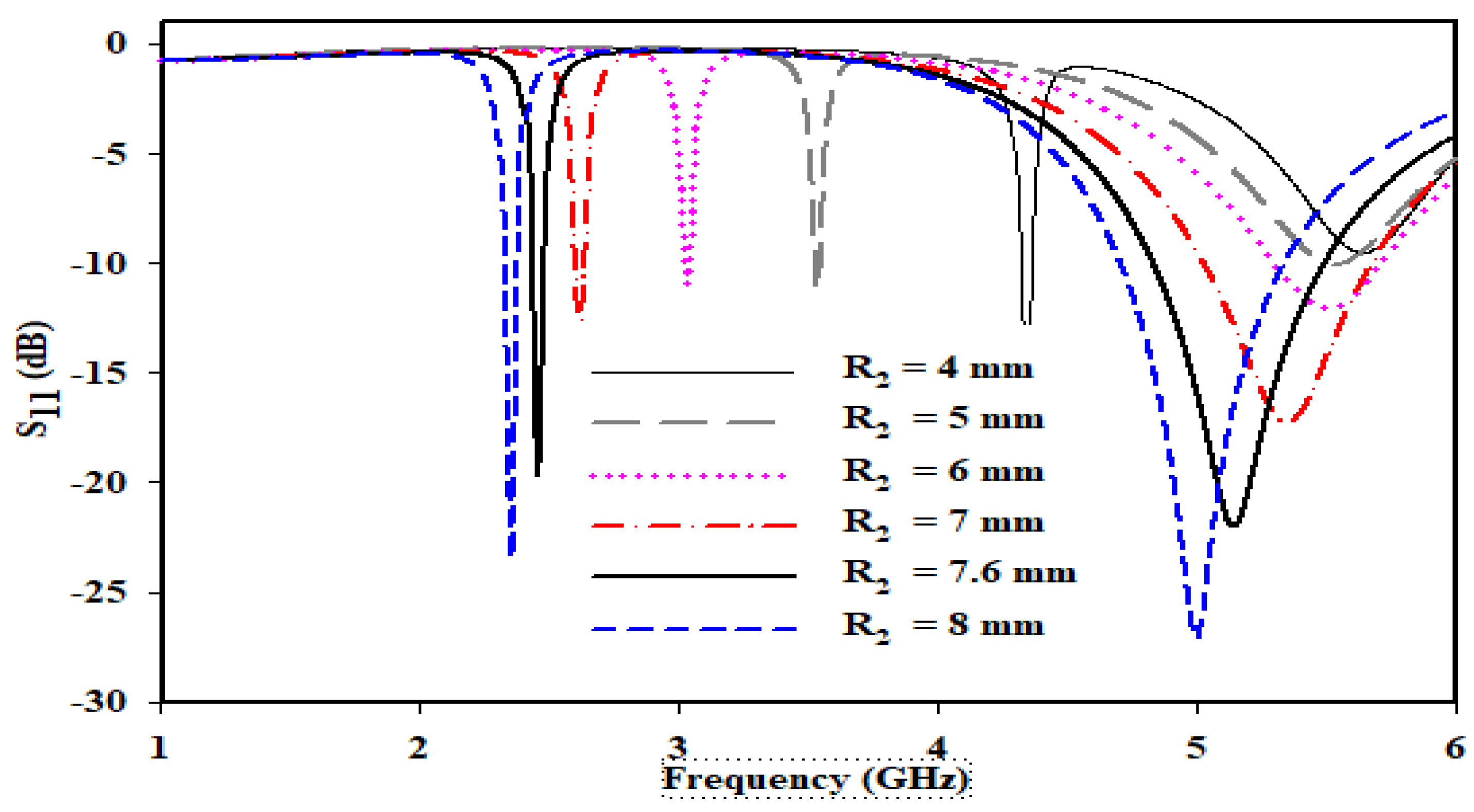
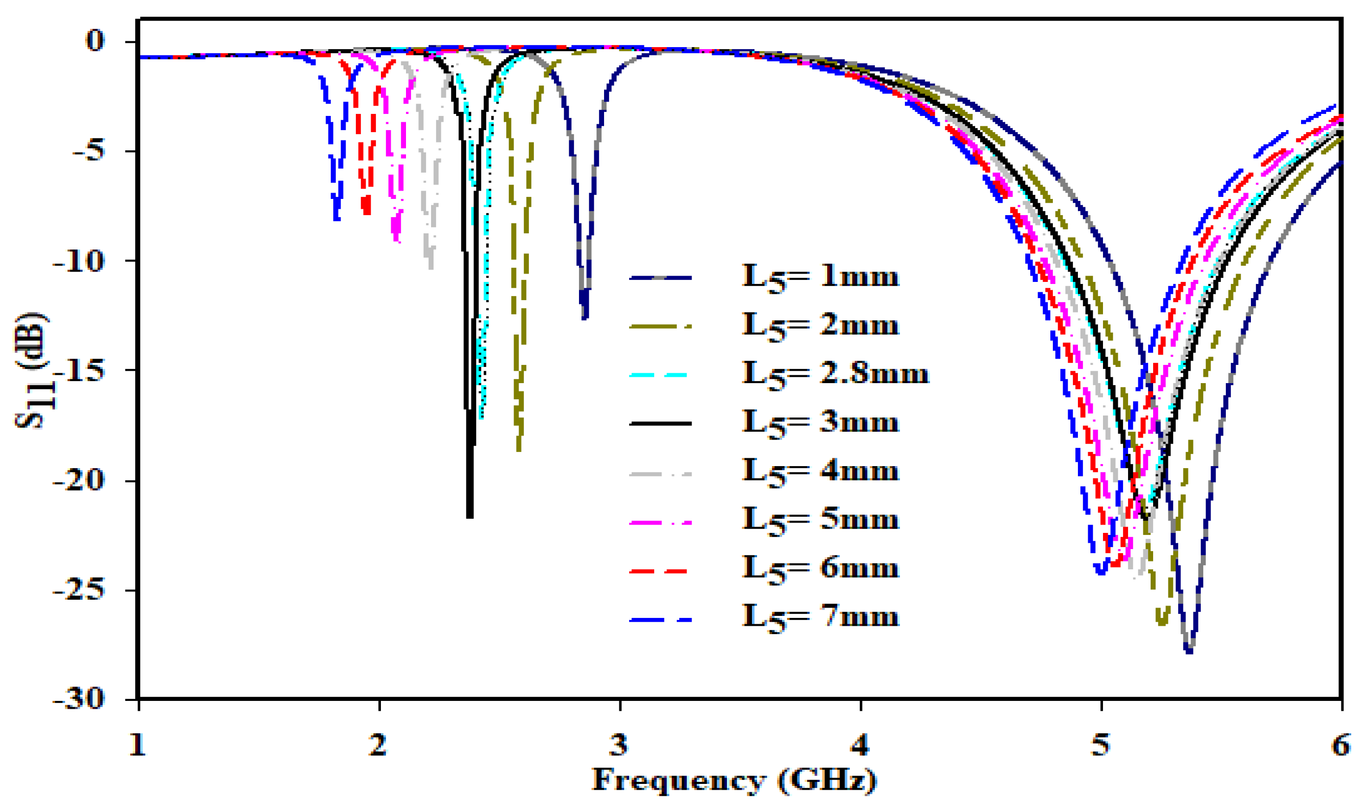
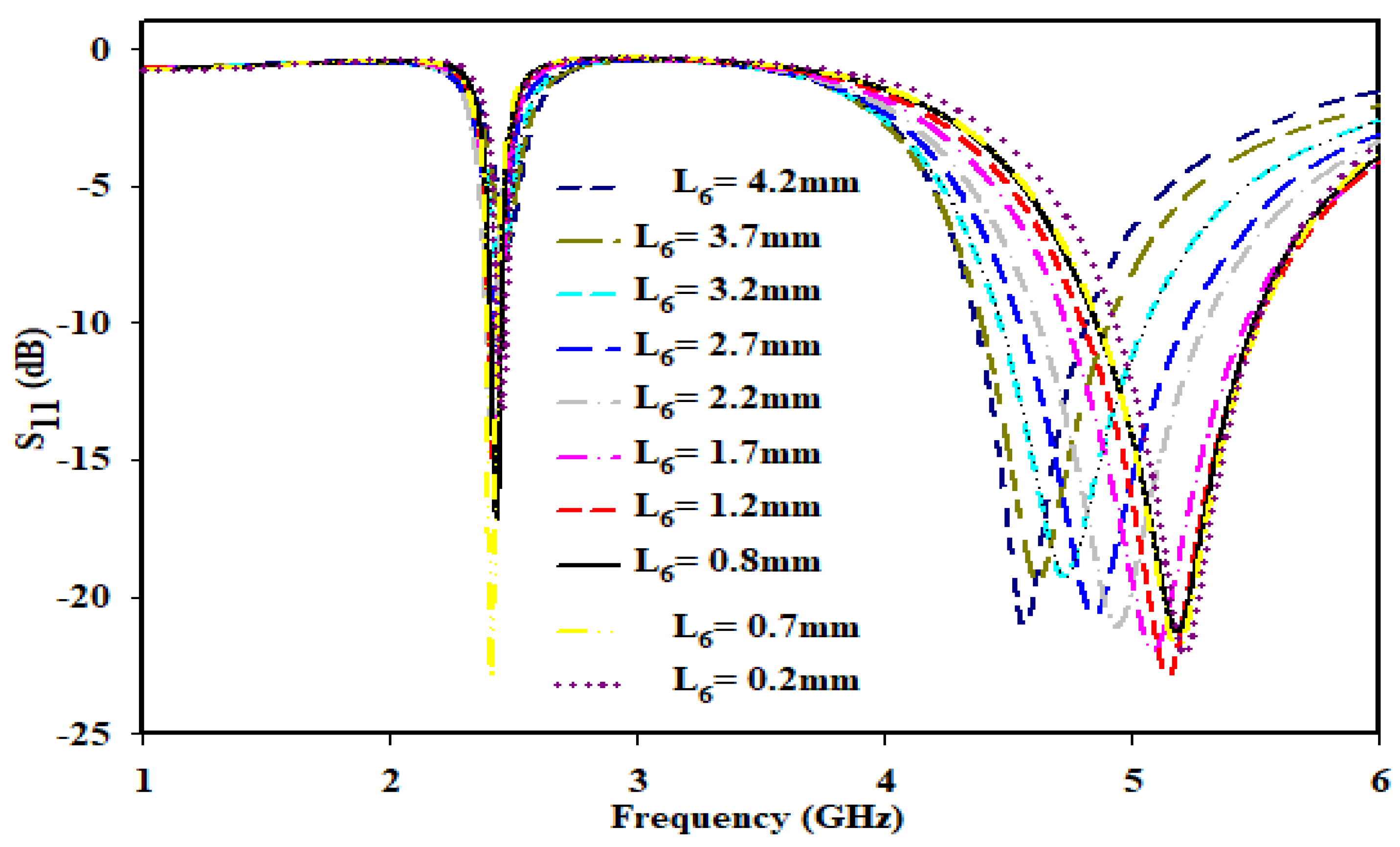
5. Parametric Analysis

The antenna resonance for various parameter changes is analysed. The parametric analysis of various parameters is carried out using ANSYS® HFSS. It can be observed that the radius of the CDNG structure plays a major role in antenna resonance frequency. The slot length L4 = R2 − W2/2 also vary with change in radius. The radius change shifts the resonaces towards lower frequencies in two resonances. The variation in the resonant frequencies with respect to the radius of CDNG-MTM (R2), keeping all other parameters constant, is illustrated in Figure 9. The parametric analysis shown as Figure 9 points out that the shift in lower band is more significant when compared to the shift in the higher band. When R2 is varied from 4 mm to 8 mm, the −10 dB bandwidth of higher band is progressively enhanced.
Figure 10 represents the variation in the resonant frequency with respect to slot length (L5). When L5 is varied from 1 mm to 7 mm, shift of resonances towards left is observed at both operating frequencies. The shift in lower band is more significant when compared to the shift in the higher frequency band. Lower frequency tuning up to 1.8 GHz is possible by varying L5. However, tuning of L5 is optimised at 2.8 mm corresponding to WLAN operating frequencies of 2.4 GHz in the lower band and 5.2 GHz in the higher band.
Figure 11 represents the variation in the resonant frequency with respect to position of CDNG structure (L6). Increase in L6 shifts the upper band towards lower frequency by keeping first resonance unaltered.
From the parametric analysis we can conclude that the first resonance is solely based on the size of the CDNG-MTM. The subsequent resonance is obtained by the combined effect of patch and CDNG-MTM.

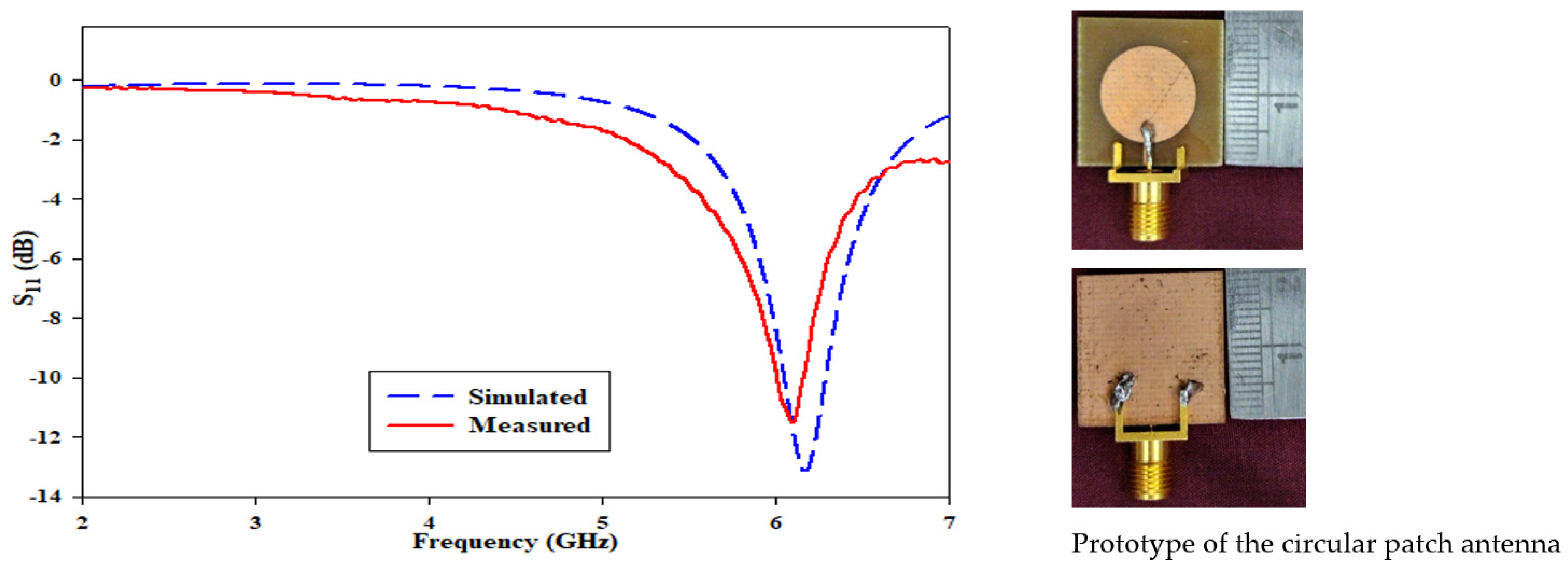
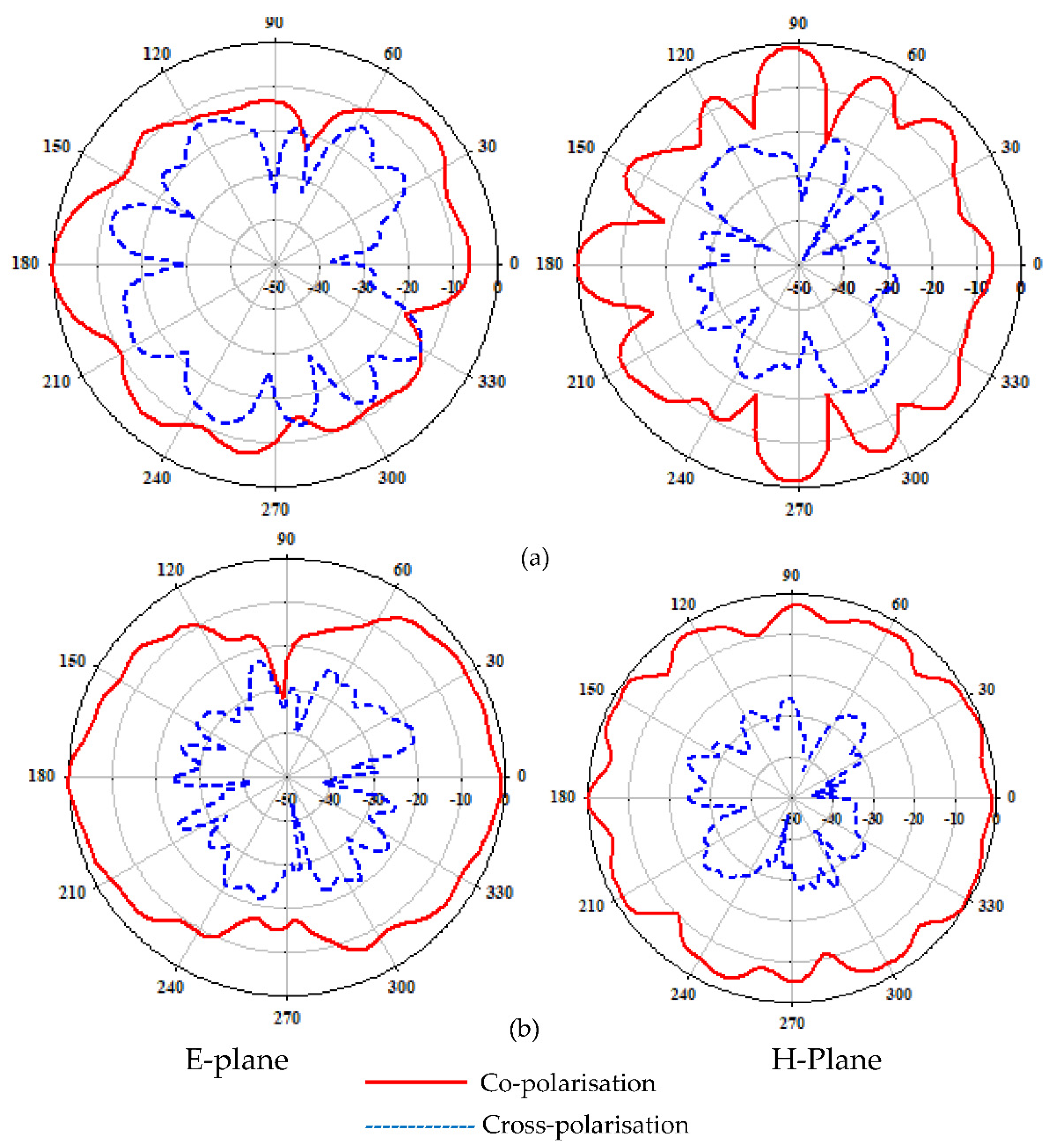
6. Experimental Validation

A prototype of the basic patch antenna and the proposed CDNG-MTM loaded ESA are fabricated on a low-cost FR-4 substrate with relative permittivity (εr) 4.4, loss tangent (tanδ) 0.02, and substrate height (h) 1.6 mm. The designed antenna is tested using a vector network analyser. All the simulations and optimisations are carried out using ANSYS® HFSS [38]. Even though the parametric analysis shows that the designed antenna can resonate up to 1.8 GHz in the lower band and 4.5 GHz in the higher band, the prototype is designed and tested at the resonance of 2.4 GHz and 5.2 GHz because they are the most commonly used application bands in wireless communications. All the mathematical calculations are done based on the lower resonance frequency 2.4 GHz. A photograph of the CDNG-MTM loaded ESA is shown in Figure 12. The simulated and measured return loss characteristics of the CDNG-MTM loaded ESA are shown in Figure 13. The figure shows that the ESA is operating at two bands with centre frequencies 2.43 GHz and 5.2 GHz. The percentage bandwidth of the basic patch antenna is 3.5%. CDNG loading results in antenna miniaturisation with enhanced bandwidth. The CDNG loaded ESA has a percentage bandwidth of 1.63% at 2.4 GHz and 13.15% at 5.2 GHz. It has, k = 51.47 rad/m at the first resonant frequency 2.4 GHz, a = 14.14 mm and therefore ka = 0.72 < 1. When these values are applied in Equation (6), the Qmin = 4.07 whereas the actual Q radiated (Qrad) obtained is 61.3%. Hence, by definition, the proposed antenna is electrically small [1].
      Q min = 1 k 3 a 3 + 1 k a
The maximum bandwidth can also be expressed using Chu limit as
  F B W max = V S W R 1 Q min V S W R
where FBWmax represents the maximum fractional bandwidth. On applying (6) and (7), the FBWmax that can be achieved at VSWR = 2, is 17.37% and the bandwidth of 1.63% obtained is well below the maximum limit of bandwidth.
Radiation characteristics of the proposed ESA at 2.4 GHz and 5.2 GHz are plotted in Figure 14. E-plane and H-plane show omni-directional characteristics in both the bands. A comparative analysis of the parameters of the basic patch with the proposed CDNG-MTM loaded antenna is presented in Table 2. The comparison shows that the proposed modified structure has distinct advantages in terms of size, operating bands, and bandwidth.
A comparative study of different types of electrically small antennas in terms of overall size, ka value, percentage miniaturisation, resonant frequency, gain, number of bands, and percentage bandwidth is summarized in Table 3. The comparison of the overall size of the antenna is done in terms of ‘λ’ wherever available, because it standardizes the electrical size of different antennas operating in different frequencies. A comparison of the overall size of various antennas reveals that all the antennas are larger than the proposed one. In conventional antennas, the increase in substrate permittivity normally decreases the antenna size. In the proposed antenna, the introduction of the CDNG-MTM on the FR4 substrate alters its permittivity so that the size of the antenna is reduced more considerably than the size reduction achieved by other MTM based antennas in Table 3. The proposed ESA is MTM inspired and it can be observed that it is better than the references in terms of size, percentage bandwidth, and multiband characteristics.

7. Conclusions

A new CDNG-MTM structure has been designed and characterised in order to develop an MTM inspired circular patch antenna. The proposed antenna has been derived from a circular patch antenna having operating frequency 6.2 GHz. The CDNG-MTM structure is loaded on the circular patch antenna and it functions as a controlling structure that can successfully manipulate the resonance behaviour of the patch. The CDNG-MTM loading has enabled the antenna to operate in two lower bands at 2.4 GHz and 5.2 GHz with percentage bandwidth of 1.63% and 13.15% respectively. The proposed CDNG-MTM structure loaded electrically small circular patch antenna enables dual-band operation with a compact size of 20 × 20 mm2 and is fabricated on low cost FR4 substrate. The loading of CDNG-MTM structure results in percentage miniaturisation of 60.7% with reasonable gain. The parametric analysis of the various design parameters has been done in order to understand the antenna’s performance in terms of resonance frequency. From this analysis, it has been observed that the first resonance is caused solely by the CDNG-MTM and the second resonance has been obtained by the combined effect of patch and CDNG-MTM. Performance comparison of the proposed antenna with the other metamaterial loaded microstrip patch antennas shows that the proposed antenna is capable of giving better performance in terms of size, percentage bandwidth, and dual-band characteristics. It is also confirmed that complementary MTM structures are a better solution for patch antenna miniaturisation. The antenna can be easily tuned to various wireless application bands by changing the size and position of CDNG-MTM. This type of antenna is suited to application in wireless devices.

Author Contributions

S.T. made substantial contributions to the conception, design, analysis, conducting experiments and writing the manuscript; B.P. analysed the obtained results, revised the manuscript, provided intellectual suggestions and supervised the whole research. All authors have read and agreed to the published version of the manuscript.

Funding

This research received no external funding.

Data Availability Statement

Not applicable.

Conflicts of Interest

The authors declare no conflict of interests.

References

  1. Wheeler, H.A. Fundamental Limitations of Small Antennas. Proc. IRE 1947, 35, 1479–1484. [Google Scholar] [CrossRef]
  2. Sonak, R.; Ameen, M.; Chaudhary, R.K. CPW-fed electrically small open-ended zeroth order resonating metamaterial antenna with dual-band features for GPS/WiMAX/WLAN applications. AEU Int. J. Electron. Commun. 2019, 104, 99–107. [Google Scholar] [CrossRef]
  3. Sohrabi, A.; Dashti, H.; Ahmadi-Shokouh, J. Design and analysis of a broadband electrically small antenna using characteristic mode theory. AEU Int. J. Electron. Commun. 2020, 113, 152991. [Google Scholar] [CrossRef]
  4. Sum, Y.L.; Rheinheimer, V.; Soong, B.H.; Monteiro, P.J. Scalable 2.45 GHz electrically small antenna design for metaresonator array. J. Eng. 2017, 5, 170–174. [Google Scholar] [CrossRef]
  5. Patel, R.; Desai, A.; Upadhyaya, T.K. An Electrically Small Antenna Using Defected Ground Structure for RFID, GPS and IEEE 802.11 A/B/G/S Applications. Prog. Electromagn. Res. Lett. 2018, 75, 75–81. [Google Scholar] [CrossRef] [Green Version]
  6. Kucukoner, E.M.; Cinar, A.; Kose, U.; Ekmekci, E. Electrical Size Reduction of Microstrip Antennas by Using Defected Ground Structures Composed of Complementary Split Ring Resonator. Adv. Electromagn. 2021, 10, 62–69. [Google Scholar] [CrossRef]
  7. Mahmud, M.Z.; Islam, M.T.; Misran, N.; Singh, M.J.; Mat, K. A Negative Index Metamaterial to Enhance the Performance of Miniaturized UWB Antenna for Microwave Imaging Applications. Appl. Sci. 2017, 7, 1149. [Google Scholar] [CrossRef] [Green Version]
  8. Rajni, R.; Marwaha, A. Electrically Small Microstrip Patch Antenna Loaded with Spiral Resonator for Wireless Applications. Wirel. Pers. Commun. 2017, 96, 2621–2632. [Google Scholar] [CrossRef]
  9. Smith, D.R.; Padilla, W.J.; Vier, D.C.; Nemat-Nasser, S.C.; Schultz, S. Composite medium with simultaneously negative permeability and permittivity. Phys. Rev. Lett. 2000, 84, 4184–4187. [Google Scholar] [CrossRef] [Green Version]
  10. Kumar, P.; Ali, T.; Pai, M.M.M. Electromagnetic Metamaterials: A New Paradigm of Antenna Design. IEEE Access 2021, 9, 18722–18751. [Google Scholar] [CrossRef]
  11. Ameen, M.; Chaudhary, R.K. Metamaterial CP antenna: A new technique for bandwidth-enhanced circularly polarized ZOR antenna based on ENG-TL backed coupled SSR with AMC metasurface. IEEE Antennas Propag. Mag. 2019. [Google Scholar] [CrossRef]
  12. Caloz, C.; Itoh, T. Electromagnetic Metamaterials: Transmission Line Approach and Microwave Applications; Wiley: Hoboken, NJ, USA, 2005. [Google Scholar]
  13. Ameen, M.; Chaudhary, R.K. Metamaterial-based circularly polarised antenna employing ENG-TL with enhanced bandwidth for WLAN applications. Electron. Lett. 2018, 54, 1152–1154. [Google Scholar] [CrossRef]
  14. Ziolkowski, R.W. Design, fabrication, and testing of double negative metamaterials. IEEE Trans. Antennas Propag. 2003, 51, 1516–1529. [Google Scholar] [CrossRef]
  15. Erentok, A.; Ziolkowski, R.W. Metamaterial-inspired efficient electrically small antennas. IEEE Trans. Antennas Propag. 2008, 57, 691–707. [Google Scholar] [CrossRef] [Green Version]
  16. Ziolkowski, R.W.; Jin, P.; Lin, C.C. Metamaterial-inspired engineering of antennas. IEEE. Proc. 2011, 99, 1720–1731. [Google Scholar] [CrossRef]
  17. Ameen, M.; Chaudharym, R.K. Dual-layer and dual-polarized metamaterial inspired antenna using circular-complementary split ring resonator mushroom and metasurface for wireless applications. AEU Int. J. Electron. Commun. 2020, 113, 152977. [Google Scholar] [CrossRef]
  18. Raval, F.; Kosta, Y.P.; Joshi, H. Reduced size patch antenna using complementary split ring resonator as defected ground plane. Int. J. Electron. Commun. 2015, 69, 1126–1133. [Google Scholar] [CrossRef]
  19. Rajeshkumar, V.; Raghavan, S. A compact CSRR loaded dual band microstrip patch antenna for wireless applications. In Proceedings of the 2013 IEEE International Conference on Computational Intelligence and Computing Research, Enathi, India, 26–28 December 2013. [Google Scholar]
  20. Fritz-Andrade, E.; Tirado-Mendez, J.A.; Jardon-Aguilar, H.; Flores-Leal, R. Application of complementary split ring resonators for size reduction in patch antenna arrays. J. Electromagn. Waves Appl. 2017, 31, 1755–1768. [Google Scholar] [CrossRef]
  21. Rashid, M.; Munir, M.E.; Khan, J.; Mahmood, K. Design of miniaturized multiband microstrip patch antenna using defected ground structure. Int. J. Adv. Comput. Sci. Appl. 2018, 9, 168–173. [Google Scholar] [CrossRef]
  22. Reddaf, A.; Djerfaf, F.; Ferroudji, K. Design of dual-band antenna using an optimized complementary split ring resonator. Appl. Phys. A 2019, 125, 186. [Google Scholar] [CrossRef]
  23. Yeo, J.; Lee, J. Design of a high-sensitivity microstrip patch sensor antenna loaded with a defected ground structure based on a complementary split ring resonator. Sensors 2020, 20, 7064. [Google Scholar] [CrossRef] [PubMed]
  24. Rajni, R.; Marwaha, A. CSC-SR structure loaded electrically small planar antenna. Appl. Comput. Electromagn. Soc. J. 2016, 31, 591–598. [Google Scholar]
  25. Abdalla, M.A.; Wahba, W.W.; Allam, A.A. Analysis and design of a compact CRLH inspired—Defected ground resonators for triple band antenna applications. Eng. Sci. Technol. Int. J. 2020, 23, 114–122. [Google Scholar] [CrossRef]
  26. Joshi, J.G.; Pattnaik, S.S.; Devi, S.; Lohokare, M.R. Electrically Small Patch Antenna Loaded with Metamaterial. IETE J. Res. 2010, 56, 373–379. [Google Scholar] [CrossRef]
  27. Karimbu Vallappil, A.; Khawaja, B.A.; Rahim, M.K.A.; Iqbal, M.N.; Chattha, H.T. Metamaterial-Inspired Electrically Compact Triangular Antennas Loaded with CSRR and 3 × 3 Cross-Slots for 5G Indoor Distributed Antenna Systems. Micromachines 2022, 13, 198. [Google Scholar] [CrossRef]
  28. Hasan, M.M.; Rahman, M.; Faruque, M.R.I.; Islam, M.T.; Khandaker, M.U. Electrically Compact SRR-Loaded Metamaterial Inspired Quad Band Antenna for Bluetooth/WiFi/WLAN/WiMAX System. Electronics 2019, 8, 790. [Google Scholar] [CrossRef] [Green Version]
  29. Balanis, C.A. Antenna Theory: Analysis and Design; John Wiley & Sons: New York, NY, USA, 1989. [Google Scholar]
  30. Thankachan, S.; Paul, B.; Pradeep, A.; Moolat, R. Design and Characterisation of Simple Planar Metamaterial Structure with Double Negative Properties. In Proceedings of the TENCON 2019— 2019 IEEE Region 10 Conference (TENCON), Kochi, India, 17–20 October 2019; pp. 1231–1235. [Google Scholar]
  31. Ekmekci, E.; Turhan-Sayan, G. Comparative Investigation of Resonance Characteristics And Electrical Size Of The Double-Sided Srr, Bc-Srr And Conventional Srr Type Metamaterials For Varying Substrate Parameters. Prog. Electromagn. Res. B 2009, 12, 35–62. [Google Scholar] [CrossRef] [Green Version]
  32. Marqus, R.; Martn, F.; Sorolla, M. Metamaterials with Negative Parameters; John Wiley & Sons, Inc.: Hoboken, NJ, USA, 2008. [Google Scholar]
  33. Li, Z.; Aydin, K.; Ozbay, E. Determination of the effective constitutive parameters of bianisotropic metamaterials from reflection and transmission coefficients. Phys. Rev. E Stat. Phys. Plasmas Fluids Relat. Interdiscip. Top. 2009, 79, 026610. [Google Scholar] [CrossRef]
  34. Zsolt, S.; Park, G.H.; Ravi, H.; Li, E.-P. A unique extraction of metamaterial parameters based on Kramers–Kronig relationship. IEEE Trans. Microw. Theory Tech. 2010, 58, 2646–2653. [Google Scholar]
  35. Smith, D.R.; Vier, D.C.; Koschny, T.; Soukoulis, C.M. Electromagnetic parameter retrieval from inhomogeneous metamaterials. Phys. Rev. E 2005, 71, 036617. [Google Scholar] [CrossRef] [Green Version]
  36. Numan, A.B.; Sharawi, M.S. Extraction of Material Parameters for Metamaterials Using a Full-Wave Simulator [Education Column]. IEEE Antennas Propag. Mag. 2013, 55, 202–211. [Google Scholar] [CrossRef]
  37. Chen, X.; Grzegorcezyk, T.M.; Wu, B.; Pacheco, J., Jr.; Kong, J.A. Robust Method to Retrieve the Constitutive Effective Parameters of Metamaterials. Phys. Rev. E 2004, 70, 016608. [Google Scholar] [CrossRef] [PubMed] [Green Version]
  38. ANSYS High Frequency Structure Simulator (HFSS); Version 15; Ansys Corporation: Pittsburgh, PA, USA, 2015.
Figure 1. Structure of the proposed circular patch antenna (a) top view (b) bottom view.
Applsci 12 03035 g001
Figure 2. Simulated and measured return loss characteristics of the circular patch antenna.
Applsci 12 03035 g002
Figure 3. S-parameters retrieval waveguide setup.
Applsci 12 03035 g003
Figure 4. S11 and S21 (a) magnitude and (b) phase plots of the CDNG structure.
Applsci 12 03035 g004
Figure 5. Retrieved results for: (a) relative permittivity ɛ and relative permeability µ; (b) refractive index n and impedance z.
Applsci 12 03035 g005
Figure 6. Structure of the proposed antenna. (a) Top view. (b) Bottom view.
Applsci 12 03035 g006
Figure 7. Current distribution of the proposed antenna. (a) 2.43 GHz. (b) 5.2 GHz.
Applsci 12 03035 g007
Figure 8. Gain plot of the proposed antenna with and without CDNG-MTM.
Applsci 12 03035 g008
Figure 9. Variation in resonant frequency with respect to radius of CDNG-MTM.
Applsci 12 03035 g009
Figure 10. Variation in resonant frequency with respect to slot length.
Applsci 12 03035 g010
Figure 11. Variation in resonant frequency with respect to position of CDNG-MTM.
Applsci 12 03035 g011
Figure 12. Prototype of the proposed ESA. (a) Top view. (b) Bottom view.
Applsci 12 03035 g012
Figure 13. Simulated and measured return loss characteristics of the proposed ESA.
Applsci 12 03035 g013
Figure 14. Radiation characteristics of the proposed ESA at (a) 2.4 GHz and (b) 5.2 GHz.
Applsci 12 03035 g014
Table 1. Design parameters of the proposed antenna.
ParametersSize (mm)ParametersSize (mm)
L120W11
L220W20.6
L33.1G10.35
L47.3G20.5
L52.8R16.5
L60.8R27.6
Table 2. Performance comparison of the proposed antenna with the basic patch antenna.
AntennaNo. of BandsFrequency (GHz)Size (λ0)ka ValueImp. BW(%)Gain
(dBi)
Patch16.2 0.417 × 0.4171.83.5%6
Patch with CDNG22.4
5.2
0.164 × 0.1640.72
1.54
1.63%
13.15%
3.8
2.9
Table 3. Performance comparison of the proposed antenna with the other microstrip patch antennas loaded with metamaterial.
Reference/YearOverall Size |(λ2 & mm2)Permittivity and Thicknesska% MiniaturisationResonant Frequency (GHz)Gain
(dBi)
No. of Bands%BW
[5]/
2018
-
20 × 21
4.4
1.6
0.75-0.926
1.57
2.47
0.32
1.2
1.5
3-
[6]/
2021
-
60 × 70
3
1.524
0.7944.941.361.7711.13
[8]/
2017
0.197 × 0.246
4 × 5
2.2
2.6
0.98-14.767.1617.96
[20]/
2017
-
40.7 × 61
2.2
1.27
-2426.31-
[22]/
2019
-
40 × 20
4.4
1.6
-81.32.4
5
1.89
3.47
2-
[24]/
2016
0.177 × 0.243
4 × 5.5
2.2
2.36
0.943-13.257.0917.96
[25]/
2020
-
100 × 100
4.4
1.6
-502.4
2.9
4.38
3.28
−4.5–3.1
3-
[26]/
2010
0.161 × 0.192
-
2.2
3.175
0.775-9.513.215.37
Proposed0.164 × 0.164
20 × 20
4.4
1.6
0.7260.72.4
5.2
3.8
2.9
21.63
13.15
Publisher’s Note: MDPI stays neutral with regard to jurisdictional claims in published maps and institutional affiliations.

