Abstract
We investigated the low-temperature direct bonding of SiC/Si via O plasma activation. After optimization, a high bonding efficiency of over 90% was obtained. Surface activation was achieved via reactive ion etching (RIE) O plasma for 30 s without significant bombardment damage. A smooth and void-free interface was observed by transmission electron microscopy (TEM), while a significant amorphous oxide layer was also detected. By increasing the annealing temperature from 150 to 300 C, the amorphous layer decreased drastically from 48 nm to 11 nm. Based on systematic experiments and analysis, the mechanism of SiC/Si low-temperature plasma-activated bonding was discussed.
1. Introduction
Silicon carbide (SiC) has superior physical and thermal properties, including a large energy band gap, high breakdown voltage, high thermal conductivity, high electron saturation velocity, and excellent stability [1]. The combination of SiC with Si technologies ouldn have promising applications in high-temperature, high-voltage, and high-power systems [2]. In particular, SiC/Si heterojunction diodes have the potential to present superior electrical properties over Schottky barrier diodes (SBDs) [3,4,5]. By introducing a Si layer on top of the SiC substrate, gate oxide can be grown on the Si layer, which can improve the reliability of the gate oxide of SiC MOSFETs [6,7,8]. Furthermore, based on the SiC/Si structure, more applications would be possible in microelectronics and microelectromechanical systems (MEMS) and photoelectric devices [9,10].
Since the SiC/Si heterostructure was proposed, much research has been conducted. Due to the large lattice mismatch between Si and SiC, the SiC/Si heterostructure obtained by epitaxy remains problematic [3,10,11]. Neither Si films grown on SiC substrates nor SiC films on Si can overcome the lattice mismatch issues [9]. Direct wafer bonding, as a unique monolithic integration technique, can achieve the combination of two materials in spite of their crystal difference [12]. Liang et al. succeeded in creating SiC/Si heterojunctions with improved electrical properties through surface-activated bonding (SAB) [2,13,14], in which the amorphous layer in the interface was eliminated after annealing at 1000 C. However, there is a high-cost complicated system required for SAB, which has restrained its further investigation and application to the SiC/Si heterojunction. As a practical method of wafer bonding, plasma-activated bonding (PAB) can achieve low-temperature wafer bonding at low cost [15]. However, the study of PAB for SiC/Si wafer bonding has not been completed, and the bonding efficiency remains low. A high bonding area ratio of over 90% can hardly be obtained by low-temperature PAB [16]. In addition, a reasonable mechanism of low-temperature direct bonding of SiC to Si via plasma activation has not been proposed.
In this paper, we investigated the low-temperature direct bonding of SiC/Si via plasma activation. Reactive ion etching (RIE) O plasma was used as the plasma source to activate the bonding surfaces. The parameters of plasma activation and annealing were investigated and optimized. To characterize the bonding interface and study the bonding mechanism, specific testing methods were employed in our experiment. In particular, the comparison of the TEM results of the SiC/Si interface under different annealing temperatures was made to investigate the impact on the amorphous layer. After a series of measurements, the rational bonding mechanism of SiC/Si PAB was discussed.
2. Experiments
In the experiment, 4-inch double polished N-type 4H-SiC (thickness = 350 m) and single polished P-type Si (thickness = 500 m) substrate wafers were all sliced into 20 mm × 20 mm samples. The Si wafer was 100 oriented, and the bonding face of the 4H-SiC was the Si face (0001 oriented).
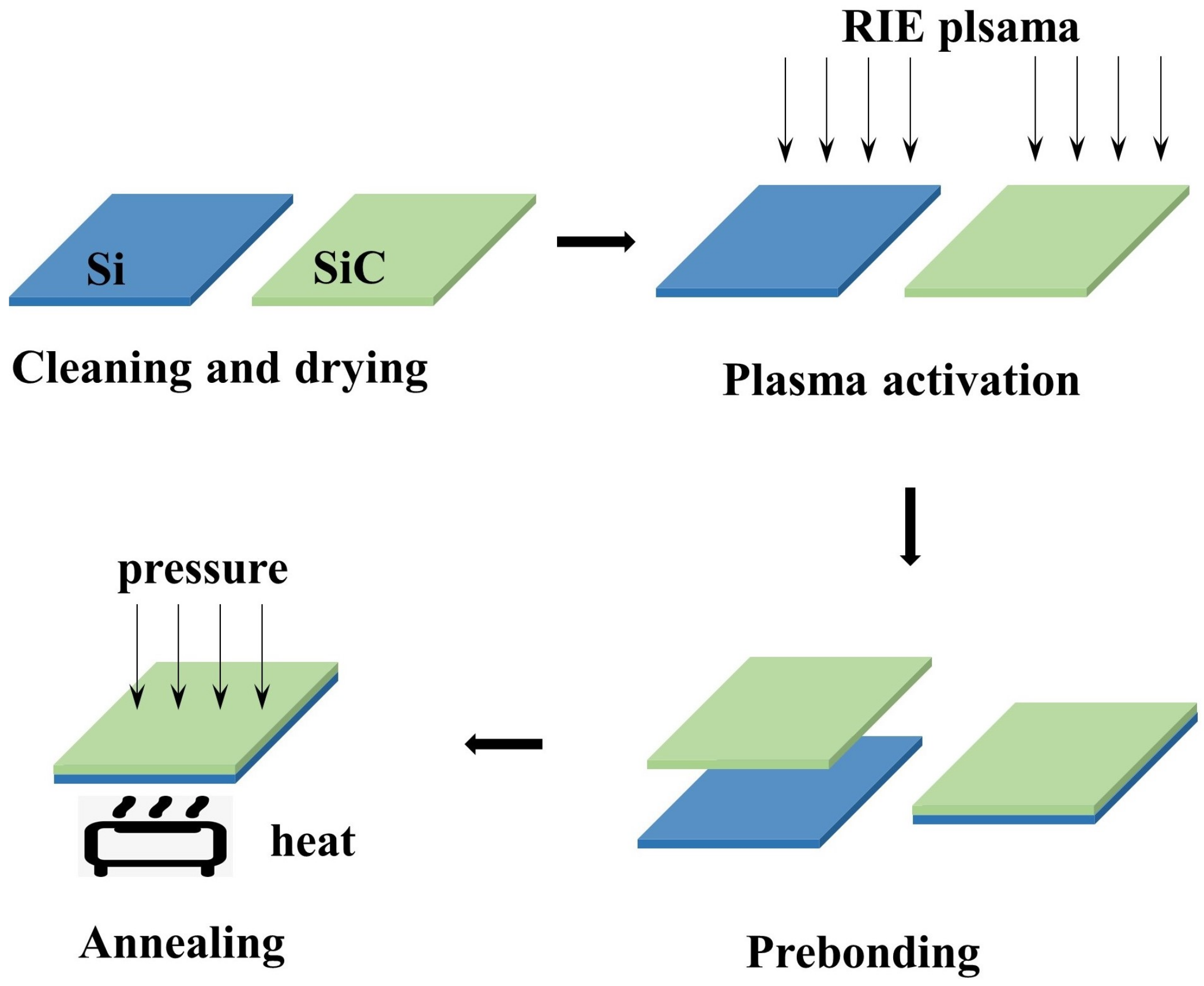
The basic process flow is demonstrated in Figure 1. The SiC and Si wafers were cleaned successively by piranha solution (HSO:HO), RCA2 (HCl:HO:HO), and diluted HF. To obtain a hydrophilic surface, the Si wafers were cleaned by NHOH:HO:HO in a ratio of 0.25:1:5 by parts, at 70 C, for 10 min. After cleaning and drying, the wafers were immediately activated by O plasma RIE. The RIE power and gas flow were set to 200 W and 50 sccm, respectively. In order to study the influence of the activation time on the bonding efficiency, the activation time was set to 0 s, 30 s, 60 s, 90 s, and 120 s, respectively. Following the plasma activation, the SiC and Si wafers were prebonded immediately. To reinforce the bonding strength, the bonded samples were annealed in the Suss MicroTec SB6e Wafer Bonder. The tool pressure of 2500 mBar and a chamber pressure of 1 × 10 mBar were applied to the prebonded samples. To study the influence of annealing time, two groups of samples were annealed at 150 C and 300 C for 3 h, respectively.
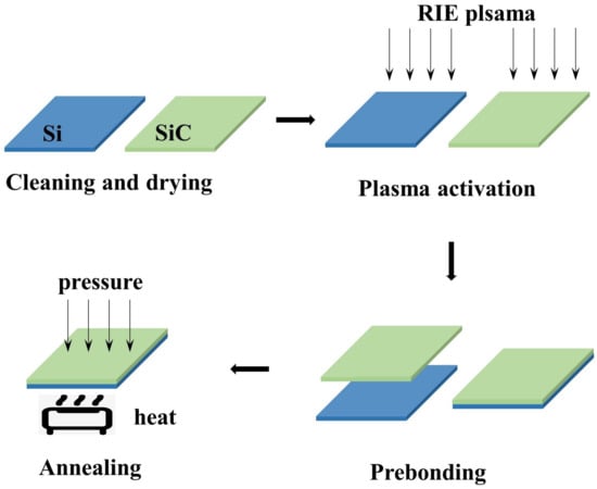
Figure 1.
Schematic diagram of the O plasma-activated bonding process.
The surface roughness of the Si and SiC samples under different activation conditions was tested by atomic force microscopy (AFM). The surface chemical states were characterized by X-ray photoelectron spectroscopy (XPS). In addition, the bonded interface SiC/Si was observed by transmission electron microscopy (TEM).
3. Results and Discussion
3.1. Effects of Bonding Parameters
Plasma activation time is a crucial parameter for PAB. The relationship between the bonding efficiency and the O plasma activation time was investigated. An efficient bonding area ratio can lead to the full combination of two different materials. Therefore, we mainly adopted the bonding area ratio to present the bonding efficiency of our experiments. A higher bonding area ratio means a better connection between the bonded samples, which is crucial for direct wafer bonding. The influence of plasma activation time and the optical images of the bonding results are shown in Figure 2.
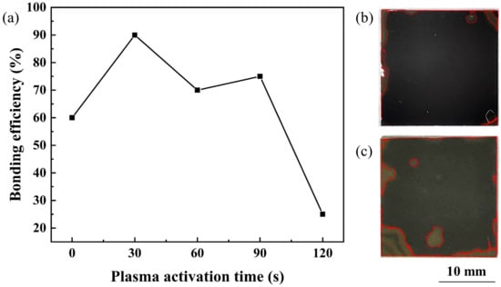
Figure 2.
(a) Bonding efficiency of SiC/Si samples as a function of O plasma activation time. Optical images of SiC/Si samples under the annealing temperature of (b) 150 C and (c) 300 C.
As the bonding results reveal in Figure 2a, when the wafer surface was not activated, the bonding area ratio was insufficient. As the activation time increased to 30 s, the bonding efficiency exceeded 90%, which was fairly high for direct bonding. Then, with the increase in activation time, the bonding efficiency showed a fluctuating decrease. After 30 s of RIE O plasma activation, the optical images of SiC/Si samples under the annealing temperatures of 150 C and 300 C are shown in Figure 2b,c, respectively. As SiC is a transparent material, the bonding area of the SiC/Si samples can be directly seen from the optical images in Figure 2b,c, in which the front layer was the SiC layer and the back was the Si layer. The unbonded region was marked, and the bonding area ratio can be calculated by its area ratio with the whole sample. Except for some inevitable voids caused by remaining contaminants, the optical images showed a fair bonding result. Therefore, 30 s of plasma activation time was adopted to further investigate the bonding mechanism.
3.2. Surface and Interface Characterizations
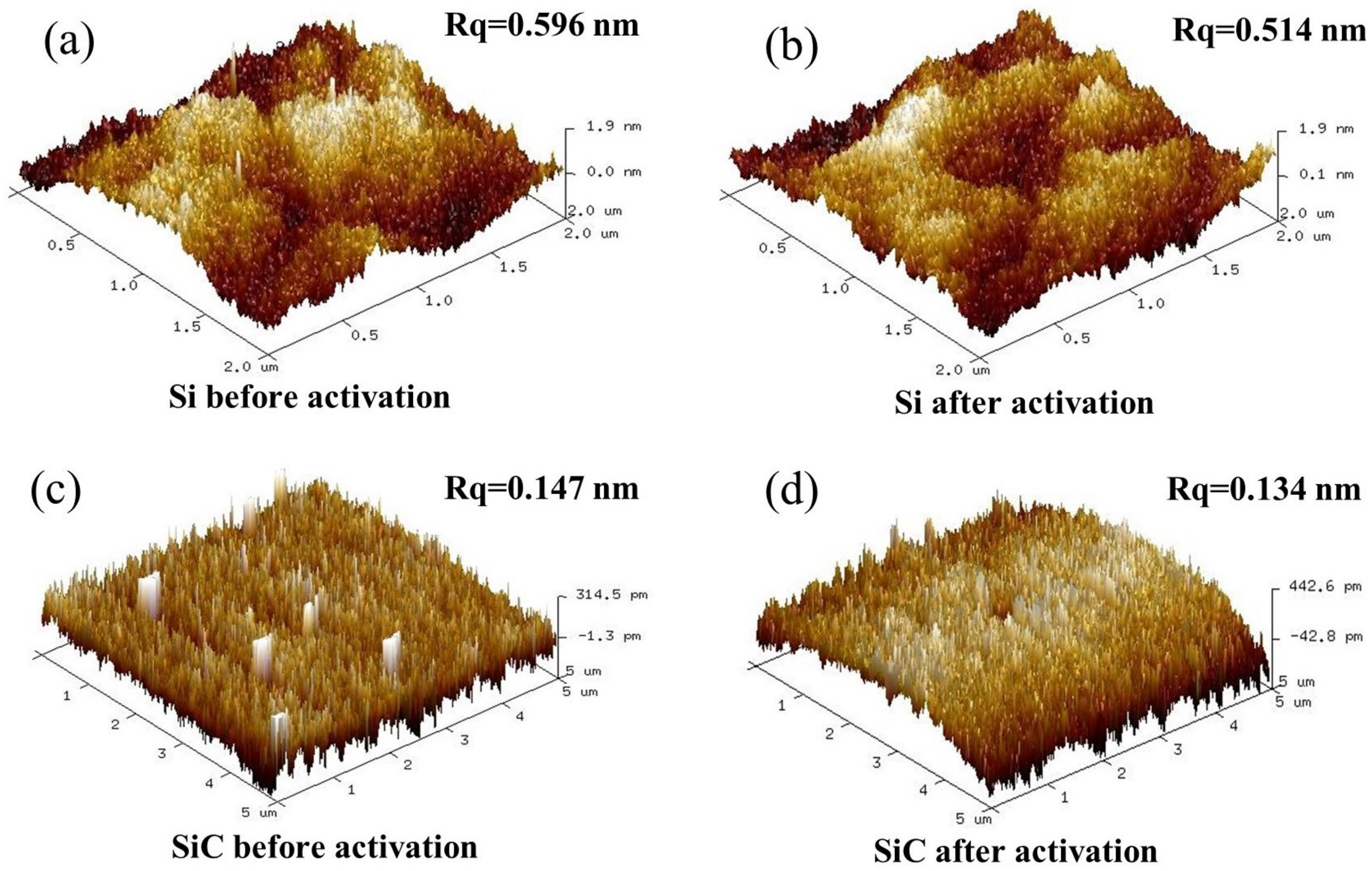
Surface roughness is an important factor for direct bonding. Surface roughness directly influences the efficiency and strength of wafer bonding. Generally, a smoother and cleaner surface will bring better bonding results [17]. Figure 3 shows the root mean square (RMS) of the Si and SiC surfaces before and after O plasma activation. After 30 s of O plasma activation, the surface roughness of the Si wafer decreased from 0.596 nm to 0.514 nm and the surface roughness of the SiC wafer decreased from 0.147 nm to 0.134 nm. According to the decrease in surface roughness, the surface of the Si and SiC wafers was cleaned by RIE plasma activation. The organic contaminants on the primary surface were diminished by the O plasma treatment. In addition, the decreased roughness might also come from the oxidation and etching of the asperity peaks. Furthermore, the three-dimensional surface morphology demonstrated that 30 s of plasma activation did not produce significant damage to the wafer surface.
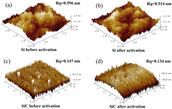
Figure 3.
Three-dimensional surface morphology with the roughness (Rq) of the Si surface before (a) and after (b) and the SiC surface before (c) and after (d) O plasma activation for 30 s.
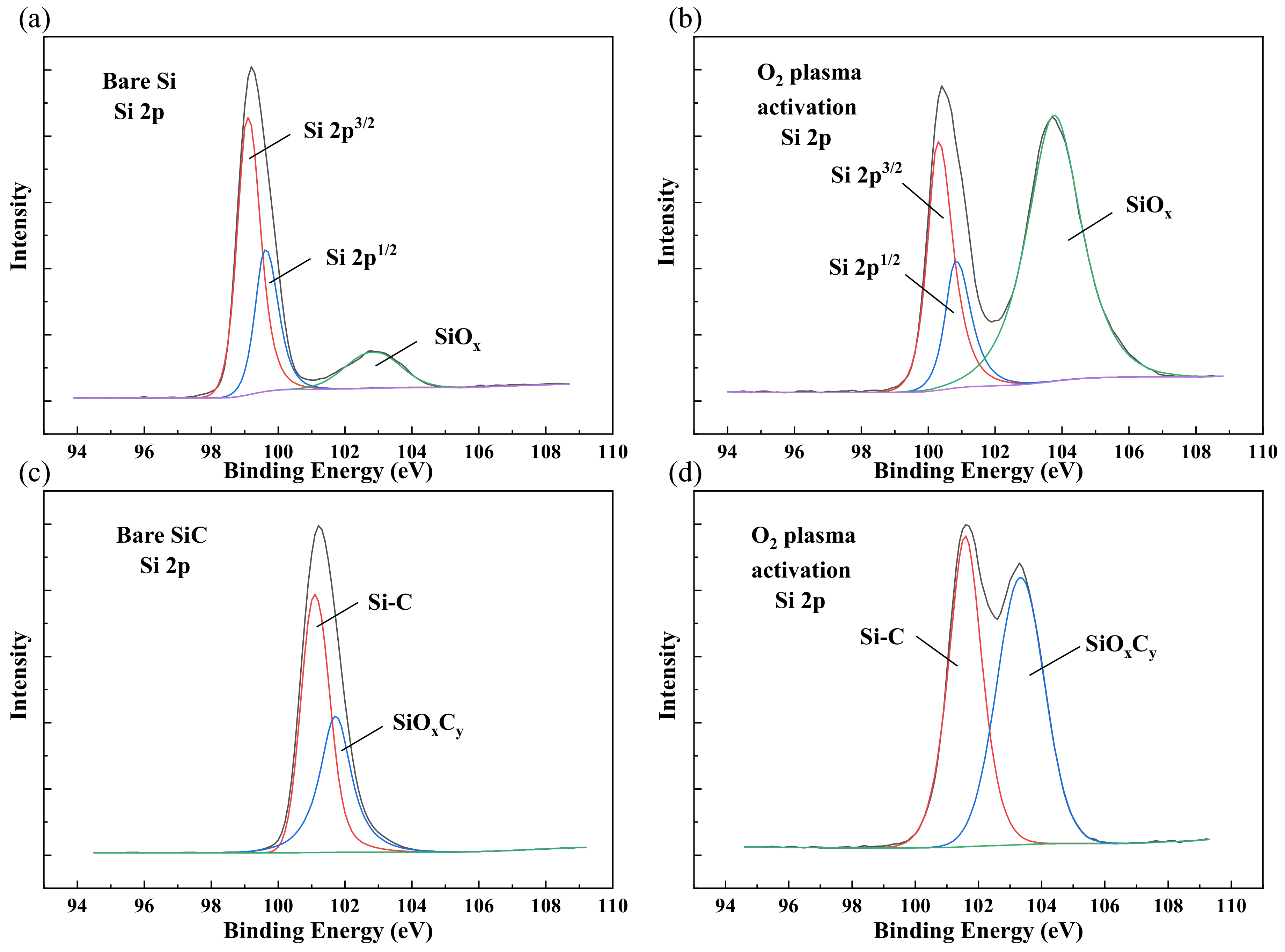
After plasma activation, the characterization of the surface chemical states was necessary to study the bonding mechanism. To investigate the surface chemical states including surface elementary composition and functional groups, X-ray photoelectron spectroscopy (XPS) was carried out. Figure 4a,b shows the Si 2p spectra of the Si surface. The main peaks were Si 2p, Si 2p, and Si–O, respectively. After O plasma activation, the intensity of the Si–O covalent bond peak increased. This variation indicated that the O plasma broke the Si–Si bonds, and the oxidation of the Si surface was formed, which might produce more Si–O dangling bonds. With higher energy, the Si–O bonds could connect free hydroxyl groups in the atmosphere that formed Si–OH groups. These increased Si–O bonds were vital to the reformation of covalent bonds in the bonding interface during the annealing process.
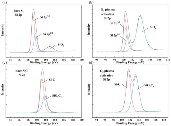
Figure 4.
XPS Si 2p spectra of (a) bare Si, (b) Si after O plasma activation, (c) bare SiC, and (d) SiC after O plasma activation.
For the SiC surface, the main peaks of Si 2p were Si–C and SiOC, as is shown in Figure 4c,d. Similar to the Si surface, the SiOC peak increased greatly after O plasma activation, which means the SiC surface was also oxided after O plasma activation. In the process of bonding and annealing, these unsaturated oxygen-containing groups can react with each other to form stable covalent bonds. In the meantime, they can also bring external oxygen into the system, which will affect the interface properties in the long run.
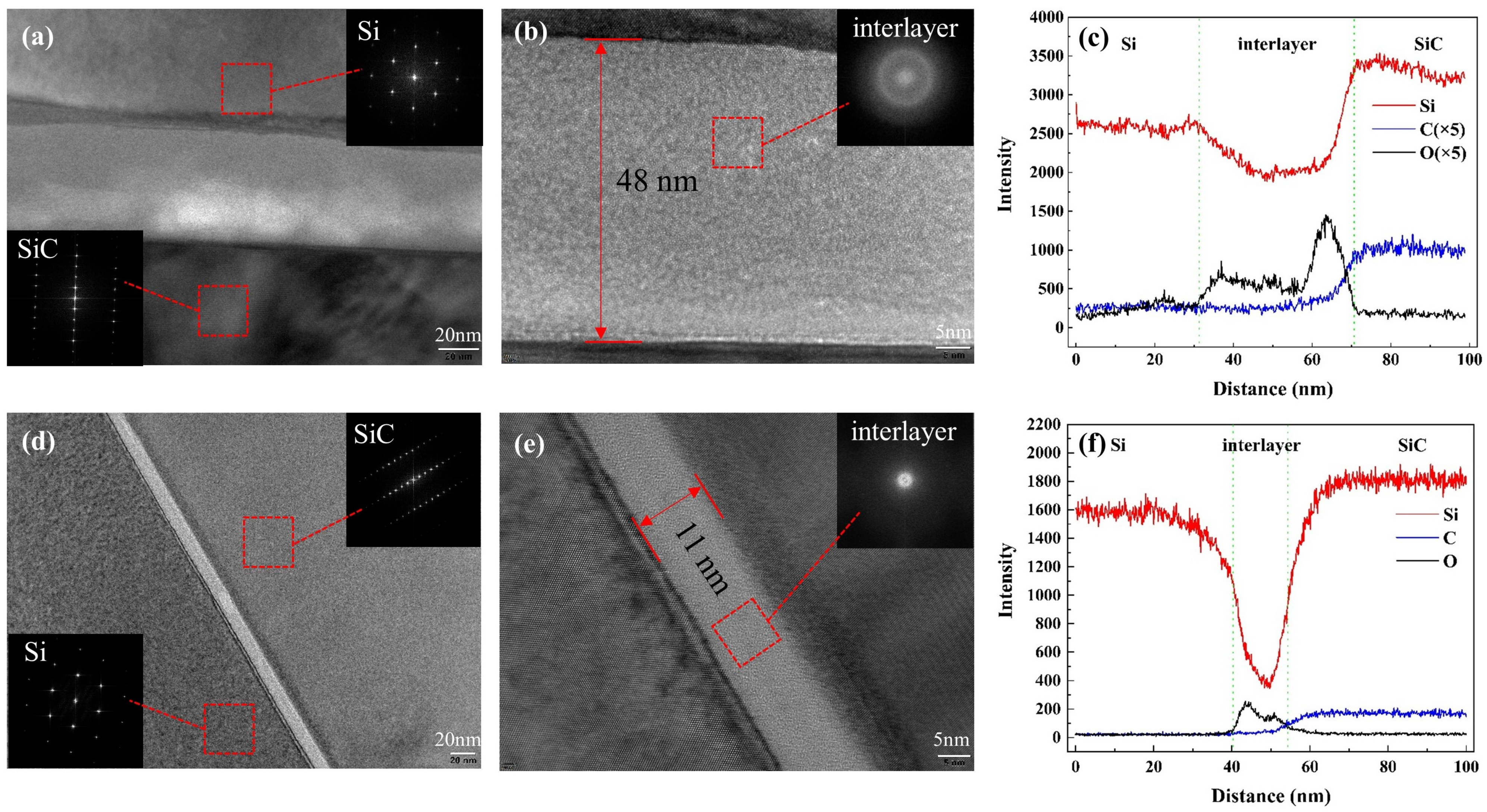
TEM was used in our experiment to characterize the bonding interface after bonding and annealing. TEM samples were fabricated by the focused ion beam (FIB) technique. The TEM images of SiC/Si bonding samples annealed at 150 C and 300 C were obtained and are shown in Figure 5.
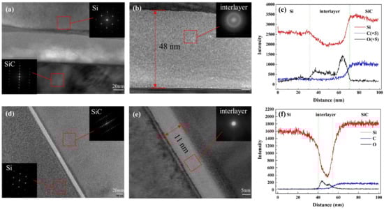
Figure 5.
Cross-sectional TEM images of the SiC/Si bonding interfaces under annealing temperatures of (a,b) 150 C and (d,e) 300 C. Element analysis across the interface with EDS line scanning of annealing at (c) 150 C and (f) 300 C.
For bonding samples annealed at 150 C, TEM images of the selected region are shown in Figure 5a,b. The lattice diffraction pattern indicated that the Si and SiC layers remained monocrystalline after bonding and annealing. From the cross-section TEM images of the SiC/Si interface, there was an obvious amorphous interlayer of 48 nm between the SiC and Si layers, which was much thicker than what was expected. In addition, the amorphous layer near the Si side was distorted, which might be caused by the oxidation of the Si layer. In order to ascertain the component of the interlayer, the element analysis of Si, O, and C was adopted by EDS. The result of EDS line analysis across the interface is shown in Figure 5c. Due to the hydrophilic bonding and O plasma activation, numerous O atoms were detected in the interlayer. From the element analysis, we can confirm that the amorphous layer basically consisted of oxide. In addition, the O plasma treatment can increase the porosity of amorphous layer, which will introduce additional absorbed water molecules [17]. When the annealing temperature was still quite low, many water molecules absorbed by the hydrophilic surface remained in the interface. The water-stored oxide layer can be responsible for the thick amorphous layer. In addition, the remaining water molecules diffused toward the Si bulk below the native oxide, which can be proved by the concentrated distribution of O atoms near the Si layer. Therefore, a curved boundary between the Si layer and oxide was detected as shown in Figure 5a.
Compared to the interface in Figure 5a,b, the interface was greatly improved when the annealing temperature increased to 300 C, as is shown in Figure 5d,e. The thickness of the amorphous layer shrank from 48 nm to 11 nm due to the increase in annealing temperature. In addition, the interface became straighter and flatter, which presented a more controllable interface. All these improvements can be attributed to the increased annealing temperature. As long as the annealing temperature was high enough, the absorbed water molecules were expelled along the interface under the chamber pressure and vacuum pressure. As the water molecules were eliminated in time, there was no additional oxide formed, and a straight boundary was obtained. However, the TEM results also demonstrated that the amorphous oxide layer cannot be eliminated for low-temperature O plasma-activated wafer bonding.
3.3. Bonding Mechanism for SiC/Si PAB
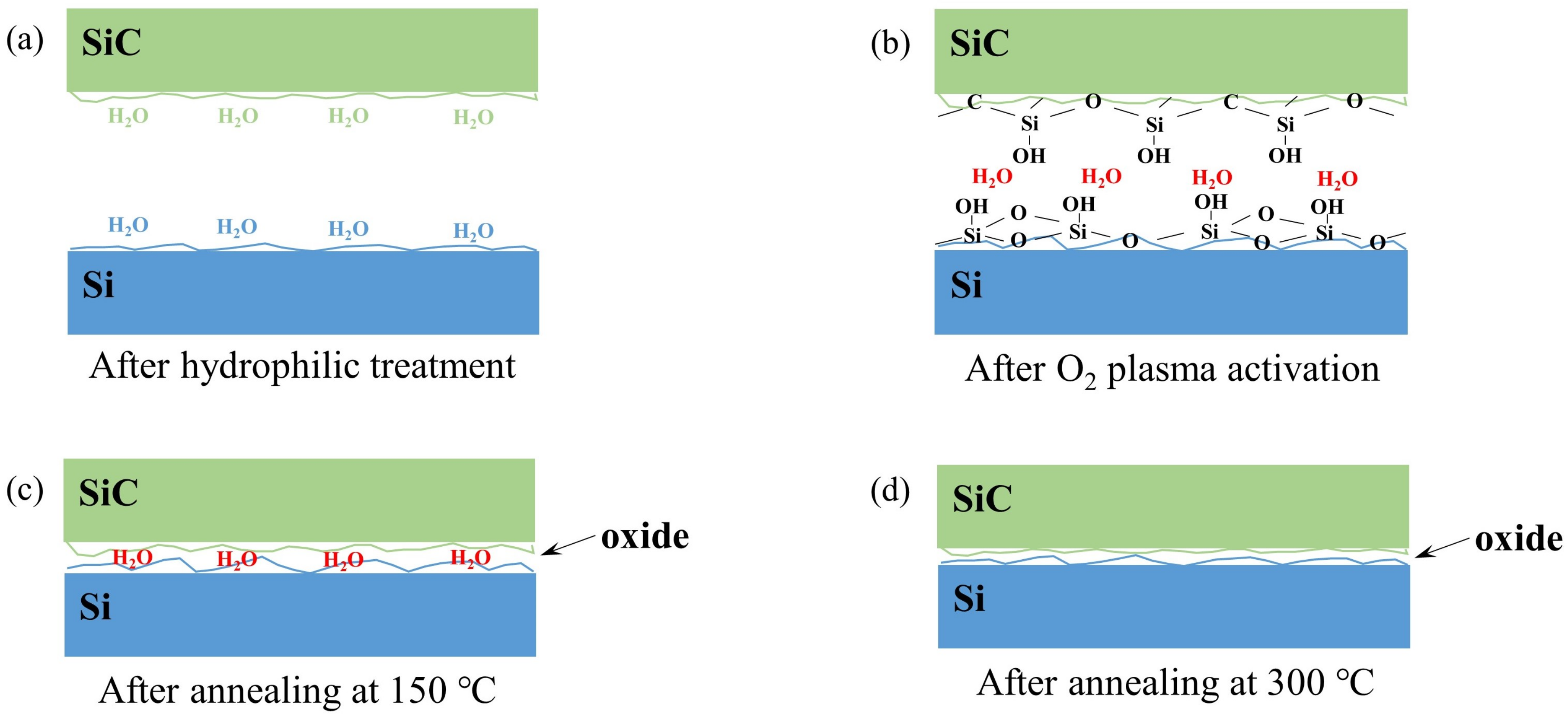
Based on our measurements and analysis, the bonding mechanism of SiC/Si PAB is discussed in this section, in which we refer to the classical PAB model for conventional Si-based bonding [17,18]. Figure 6 shows the schematic diagram of the interface during the bonding process.

Figure 6.
Schematic diagram of the SiC/Si plasma activation bonding mechanism. Interface (a) after hydrophilic treatment, (b) after O plasma activation, (c) after annealing at 150 C, and (d) after annealing at 300 C.
As a natural hydrophilic material, SiC wafers can easily absorb water molecules from the air and form silanol (Si-OH) groups after standard cleaning. For Si wafers, after being cleaned by the diluted HF solution, a hydrophobic surface was obtained. After our specific hydrophilic treatment, the Si surface regained the ability to absorb water molecules.
After RIE plasma activation, the Si–Si bonds of the Si surface and the Si–C bonds of the SiC surface were broken by O plasma. The O plasma bombardment can deform the wafer surfaces and produce many dangling bonds, increasing the actual contact area.
After prebonding at room temperature, the surfaces of SiC and Si contacted with each other. As the hydrophilic surfaces have already absorbed many water molecules from the air, during this period, the two wafers were mostly bonded by hydrogen bonds between the chemisorbed water molecules located on the opposing wafer surfaces. The reaction between dangling bonds was not strong enough to dominate the formation of the bonding interface. Therefore, the bonding strength was still quite weak.
As shown in Figure 6c, under low-temperature annealing at 150 C, the applied pressure could make full contact between the prebonded wafers. The dangling bonds and unsaturated oxygen-containing groups between the Si and SiC surfaces were connected by polymerization reactions (1) and (2).
Similar to the Si-based PAB model proposed by Plach et al. [18], the original adsorbed and reaction-generated water molecules could not be eliminated completely through the nanogaps at low temperatures. The residual water might have diffused towards the Si bulk below the native oxide, where additional oxide containing crystal water was formed. In addition, oxidation at the interface mainly occurred near the void area. Similar to the Si/SiO bonding system [19], water stress corrosion can soften the roughness asperities, which will increase the bonding area. The remaining water in the surface can also help the subsurface layer to become smoother and the roughness asperity to deform. Furthermore, the oxidation of the interface asperity will induce an increase in the asperity volume, which will help to close the interface and increase the bonding energy.
When the annealing temperature rose from 150 to 300 C, the water molecules may have either diffused out along the bonded interface or reacted with Si according to reaction (3).
Due to the high vacuum pressure and the increase in temperature, these vaporized water molecules along with hydrogen were expelled along the interface. Therefore, the thickness of the amorphous oxide layer decreased, which agreed with our TEM results in Figure 5. From the bonding mechanism, we can confirm that the oxide-free interface for SiC/Si cannot be obtained by low-temperature wafer bonding via O plasma activation. Several nanometers of the oxide layer were unavoidable, especially under low-temperature annealing.
4. Conclusions
In conclusion, we have investigated the optimal condition of plasma-activated direct bonding for SiC/Si wafers, which led to a high bonding efficiency of over 90%. Despite the high bonding area ratio, a thick amorphous layer was observed in the interface. The amorphous oxide layer will damage the electrical properties and limit its further applications. TEM results showed the impact of annealing temperature on the amorphous layer. When the annealing temperature increased from 150 to 300 C, the amorphous oxide layer decreased immensely. In addition, based on our investigation, the mechanism of SiC/Si low-temperature PAB was discussed in detail. However, due to the restraint of the low vacuum and low annealing temperature, the amorphous layer of bonded wafers obtained by low-temperature PAB cannot be eliminated completely. Higher annealing temperature and superior activation source must be applied to avoid the oxide layer in the interface.
Author Contributions
Conceptualization, F.W.; methodology, F.W.; validation, Y.Z., J.W. and Z.G.; investigation, F.W. and Y.Z.; resources, X.Y.; data curation, J.W.; writing—original draft preparation, F.W.; writing—review and editing, Z.F. and Z.H.; visualization, X.Y.; supervision, Z.H. and F.Y.; project administration, Z.F.; funding acquisition, Z.F. All authors have read and agreed to the published version of the manuscript.
Funding
This research was supported by the National Key Research and Development Program (No. 2016YFB0400500), and the Science & Technology Program of the State Grid Corporation of China Co., Ltd. “High voltage and high power SiC materials, devices and the application demonstration in power electronic transformers”.
Institutional Review Board Statement
Not applicable.
Informed Consent Statement
Not applicable.
Data Availability Statement
Not applicable.
Acknowledgments
The author Fengxuan Wang would like to thank Zhen Huang for support during the writing of the manuscript.
Conflicts of Interest
The authors declare no conflict of interest.
References
- Bhatnagar, M.; Baliga, B.J. Comparison of 6H-SiC, 3C-SiC, and Si for power devices. IEEE Trans. Electron Devices 1993, 40, 645–655. [Google Scholar] [CrossRef]
- Liang, J.; Nishida, S.; Arai, M.; Shigekawa, N. Effects of thermal annealing process on the electrical properties of p+-Si/n-SiC heterojunctions. Appl. Phys. Lett. 2014, 104, 161604. [Google Scholar] [CrossRef] [Green Version]
- Pérez-Tomás, A.; Jennings, M.; Davis, M.; Covington, J.; Mawby, P.; Shah, V.; Grasby, T. Characterization and modeling of n-n Si/ SiC heterojunction diodes. J. Appl. Phys. 2007, 102, 014505. [Google Scholar] [CrossRef]
- Wang, Y.; Wang, H.Y.; Cao, F.; Wang, H.Y. High performance of polysilicon/4H-SiC dual-heterojunction trench diode. IEEE Trans. Electron Devices 2017, 64, 1653–1659. [Google Scholar] [CrossRef]
- Guy, O.J.; Jenkins, T.; Lodzinski, M.; Castaing, A.; Wilks, S.; Bailey, P.; Noakes, T. Ellipsometric and MEIS studies of 4H-SiC/Si/SiO2 and 4H-SiC/SiO2 interfaces for MOS devices. In Materials Science Forum; Trans Tech Publications Ltd.: Bäch, Switzerland, 2007; Volume 556, pp. 509–512. [Google Scholar]
- Chan, C.; Mawby, P.A.; Gammon, P.M. Analysis of linear-doped Si/SiC power LDMOSFETs based on device simulation. IEEE Trans. Electron Devices 2016, 63, 2442–2448. [Google Scholar] [CrossRef] [Green Version]
- Pérez-Tomás, A.; Lodzinski, M.; Guy, O.; Jennings, M.; Placidi, M.; Llobet, J.; Gammon, P.; Davis, M.; Covington, J.; Burrows, S.; et al. Si/SiC bonded wafer: A route to carbon free SiO2 on SiC. Appl. Phys. Lett. 2009, 94, 103510. [Google Scholar] [CrossRef] [Green Version]
- Wang, Y.; Ma, Y.C.; Hao, Y.; Hu, Y.; Wang, G.; Cao, F. Simulation study of 4H-SiC UMOSFET structure with p+-polySi/SiC shielded region. IEEE Trans. Electron Devices 2017, 64, 3719–3724. [Google Scholar] [CrossRef]
- Li, L.; Chen, Z.; Zang, Y.; Song, L.; Han, Y.; Chu, Q. Epitaxial growth of Si/SiC heterostructures with different preferred orientations on 6H-SiC (0001) by LPCVD. CrystEngComm 2016, 18, 5681–5685. [Google Scholar] [CrossRef]
- Feng, Z.; Zhi-Ming, C.; Lian-Bi, L.; Shun-Feng, Z.; Tao, L. SiC based Si/SiC heterojunction and its rectifying characteristics. Chin. Phys. B 2009, 18, 4966. [Google Scholar] [CrossRef]
- Lianbi, L.; Zhiming, C.; Ying, Y. Hetero-epitaxy and structure characterization of Si films on 6H-SiC substrates. Mater. Lett. 2011, 65, 1257–1260. [Google Scholar] [CrossRef]
- Alexe, M.; Gösele, U. Wafer Bonding: Applications and Technology; Springer Science & Business Media: Berlin/Heidelberg, Germany, 2013; Volume 75. [Google Scholar]
- Liang, J.; Nishida, S.; Hayashi, T.; Arai, M.; Shigekawa, N. Effects of interface state charges on the electrical properties of Si/SiC heterojunctions. Appl. Phys. Lett. 2014, 105, 151607. [Google Scholar] [CrossRef] [Green Version]
- Liang, J.; Nishida, S.; Arai, M.; Shigekawa, N. Improved electrical properties of nn and pn Si/SiC junctions with thermal annealing treatment. J. Appl. Phys. 2016, 120, 034504. [Google Scholar] [CrossRef] [Green Version]
- Yeo, C.; Xu, D.; Yoon, S.; Fitzgerald, E. Low temperature direct wafer bonding of GaAs to Si via plasma activation. Appl. Phys. Lett. 2013, 102, 054107. [Google Scholar] [CrossRef]
- Kang, Q.; Wang, C.; Niu, F.; Zhou, S.; Xu, J.; Tian, Y. Single-crystalline SiC integrated onto Si-based substrates via plasma-activated direct bonding. Ceram. Int. 2020, 46, 22718–22726. [Google Scholar] [CrossRef]
- Ramm, P.; Lu, J.J.Q.; Taklo, M.M. Handbook of Wafer Bonding; John Wiley & Sons: Hoboken, NJ, USA, 2011. [Google Scholar]
- Plach, T.; Hingerl, K.; Tollabimazraehno, S.; Hesser, G.; Dragoi, V.; Wimplinger, M. Mechanisms for room temperature direct wafer bonding. J. Appl. Phys. 2013, 113, 094905. [Google Scholar] [CrossRef]
- Fournel, F.; Martin-Cocher, C.; Radisson, D.; Larrey, V.; Beche, E.; Morales, C.; Delean, P.; Rieutord, F.; Moriceau, H. Water stress corrosion in bonded structures. ECS J. Solid State Sci. Technol. 2015, 4, P124. [Google Scholar] [CrossRef]

Publisher’s Note: MDPI stays neutral with regard to jurisdictional claims in published maps and institutional affiliations. |
© 2022 by the authors. Licensee MDPI, Basel, Switzerland. This article is an open access article distributed under the terms and conditions of the Creative Commons Attribution (CC BY) license (https://creativecommons.org/licenses/by/4.0/).