
Self-Balancing Power Amplifier with a Minimal DC Offset for Launcher Automation Control Circuits of a Surface-to-Air Missile System


Abstract
:1. Introduction
2. Materials and Methods
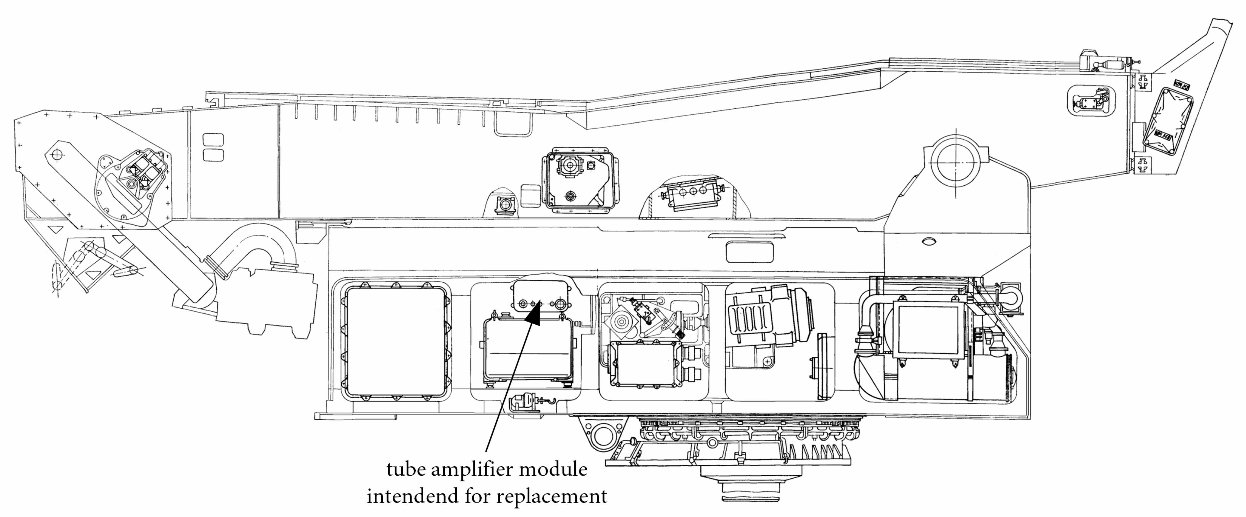
2.1. Problem Formulation: Initial Design Assumptions
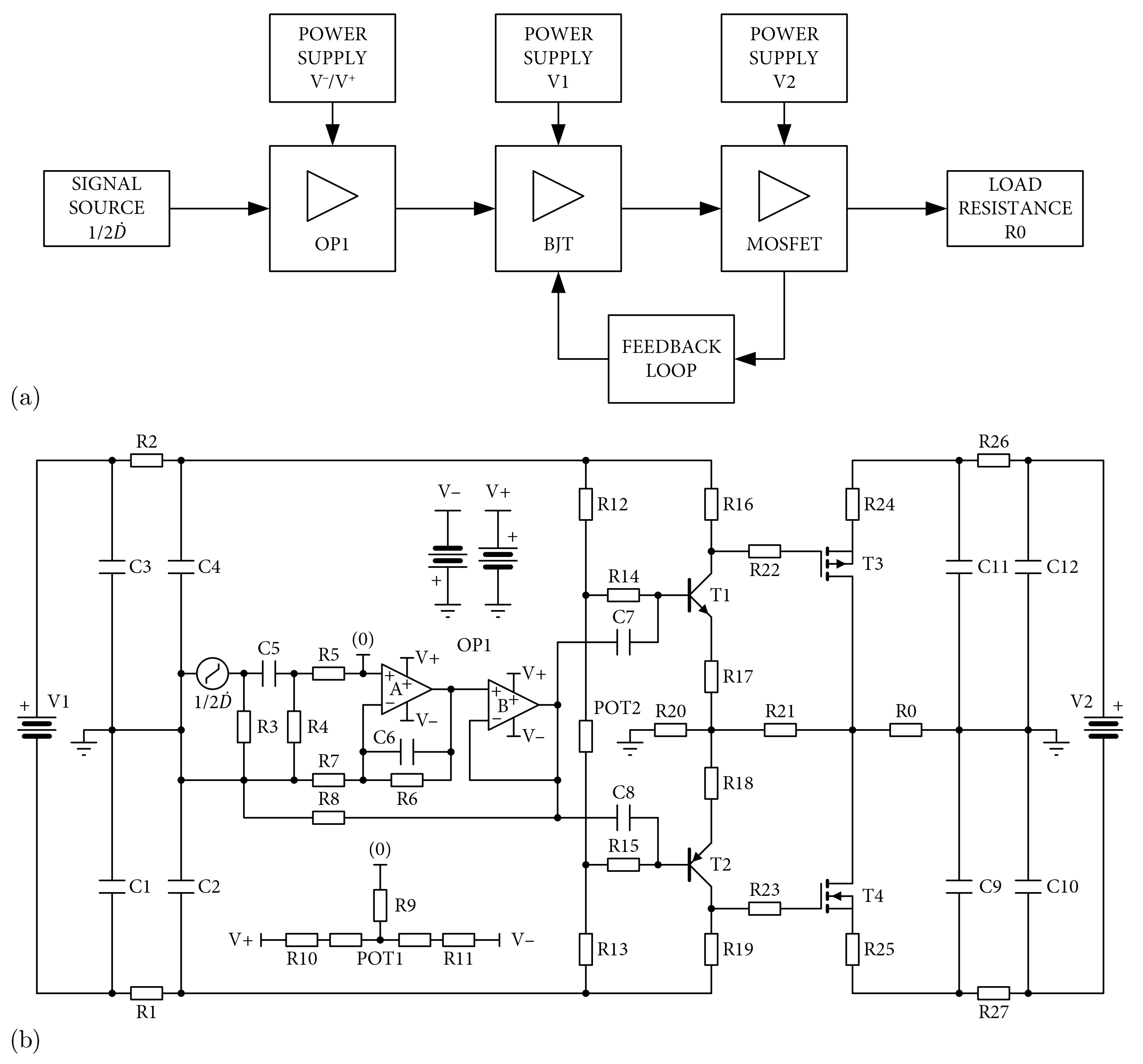
2.2. Circuit Design
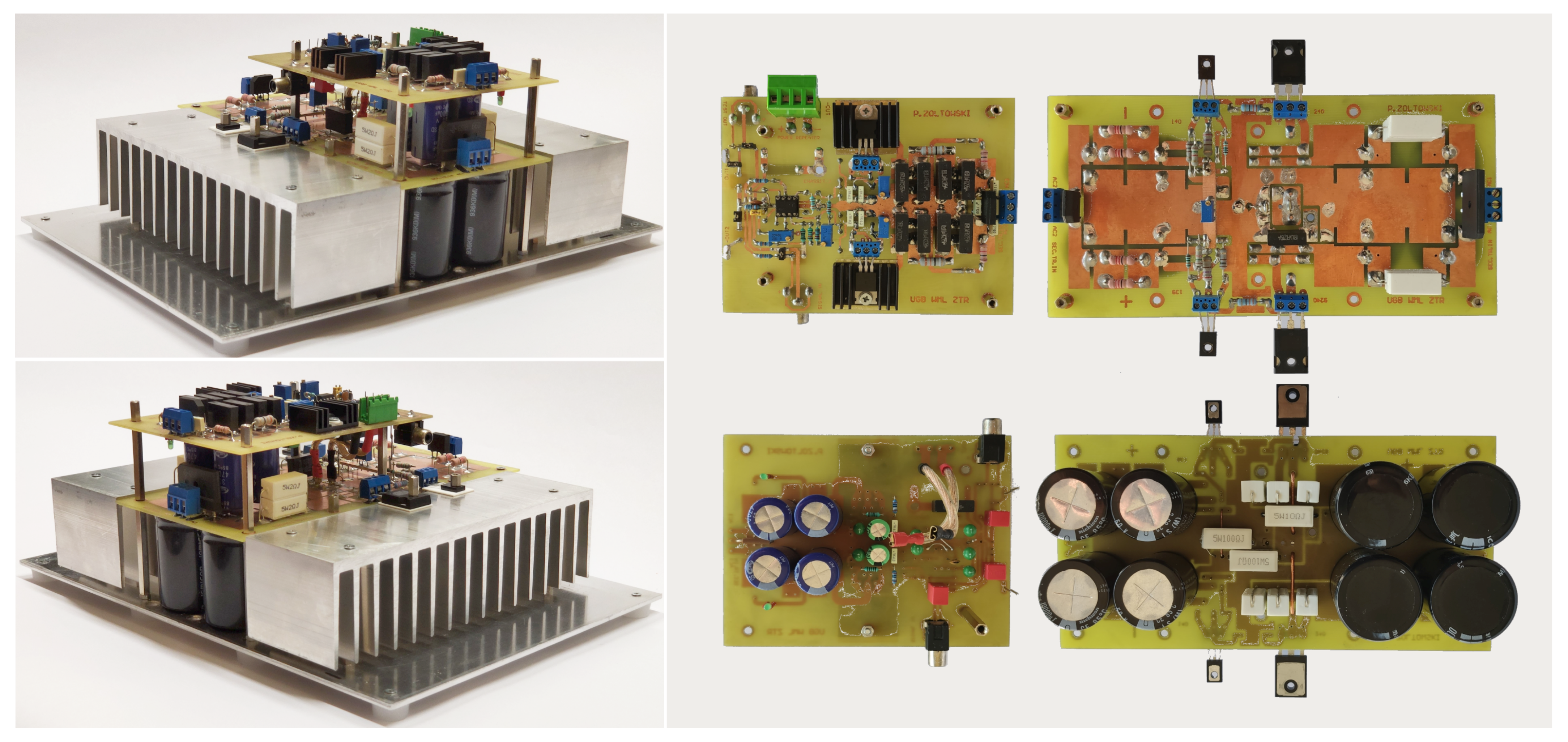
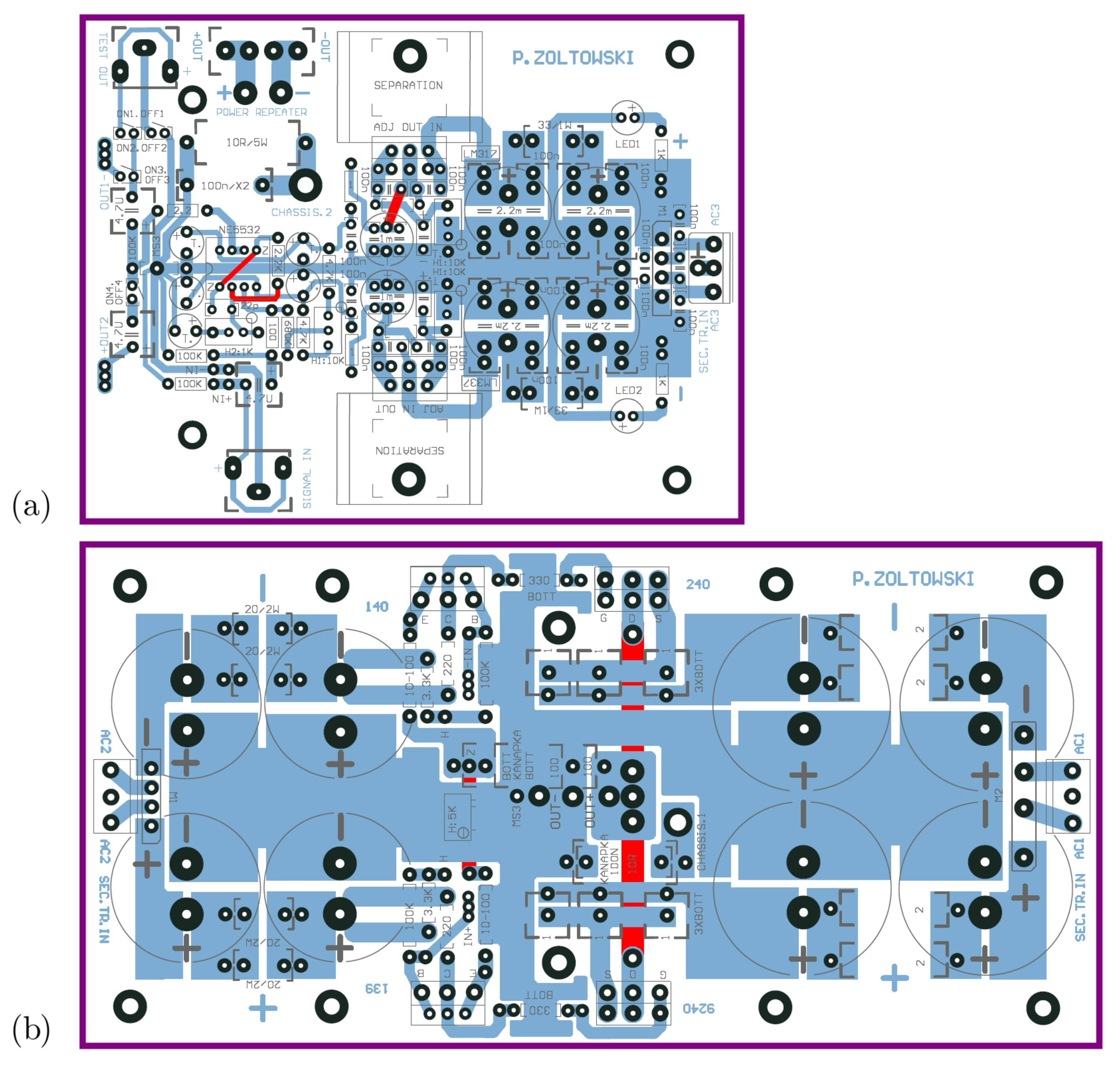
2.3. Hardware Implementation
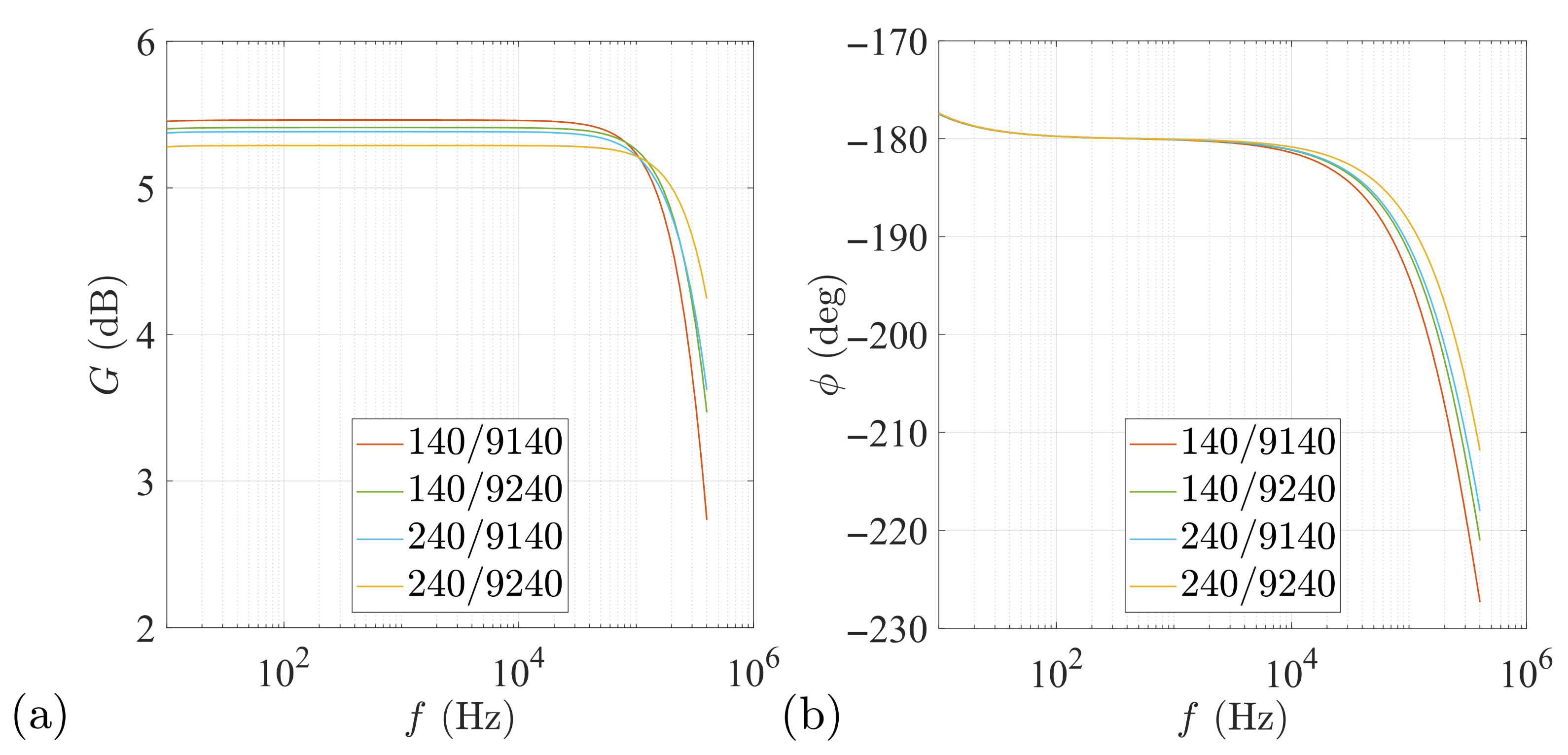
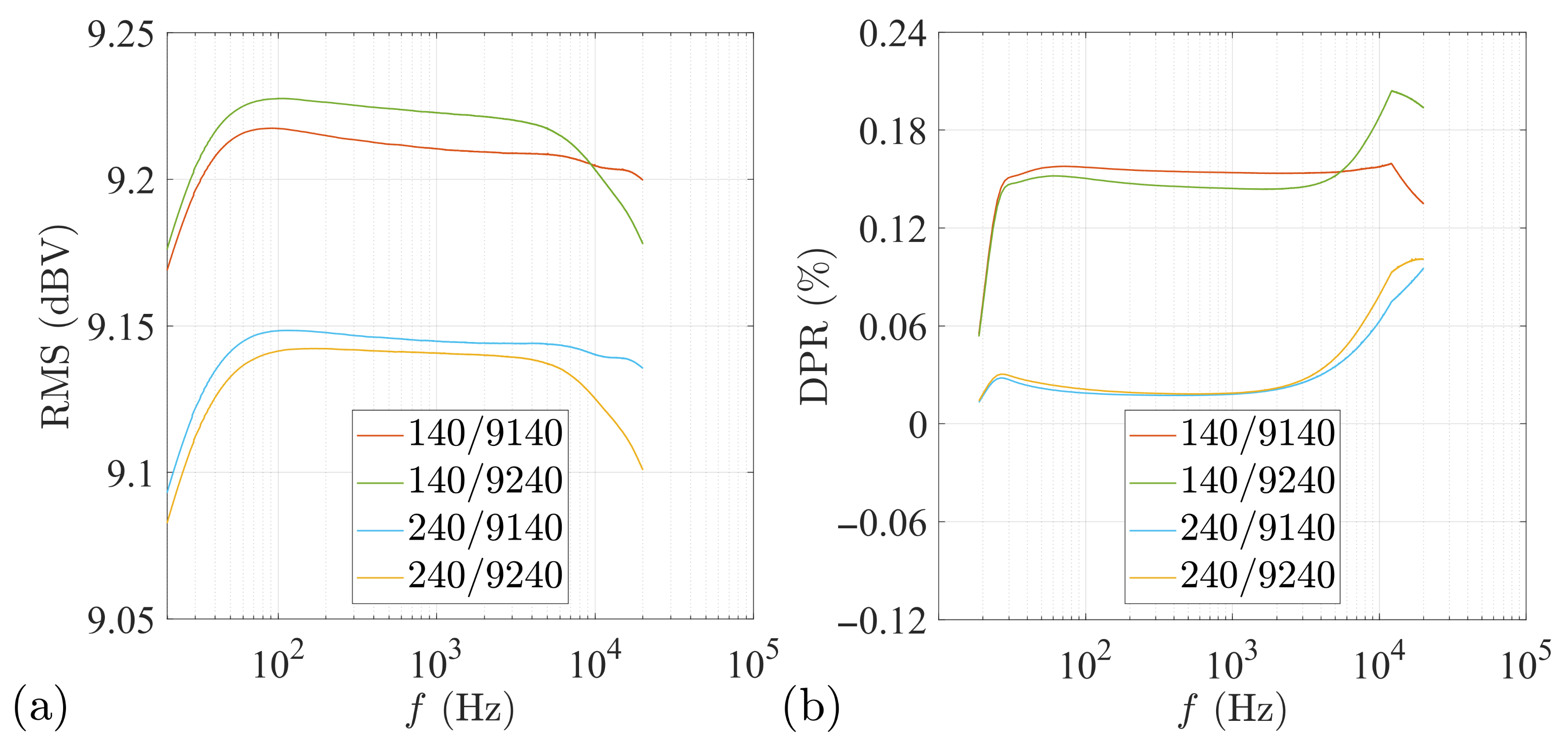
3. Results and Discussion
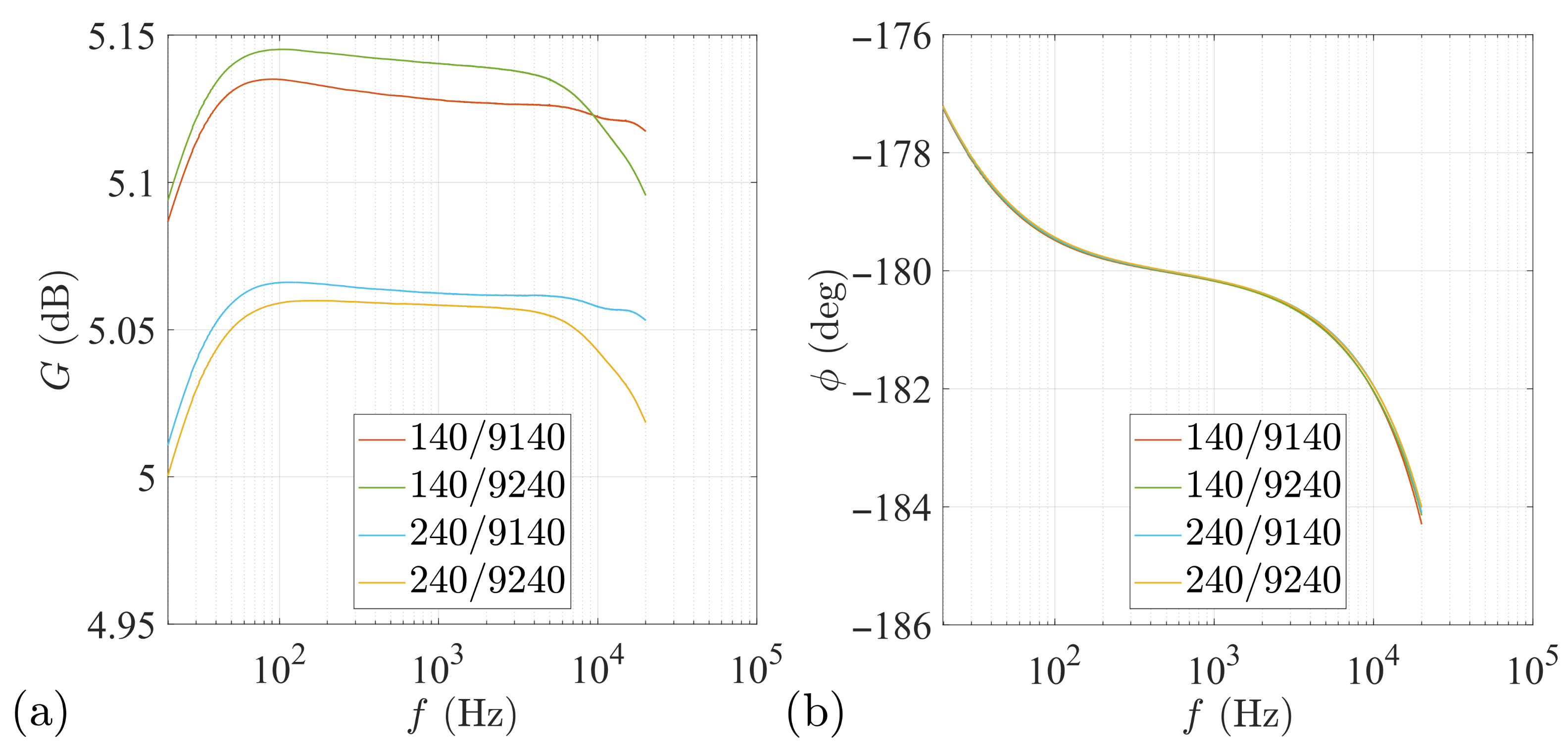
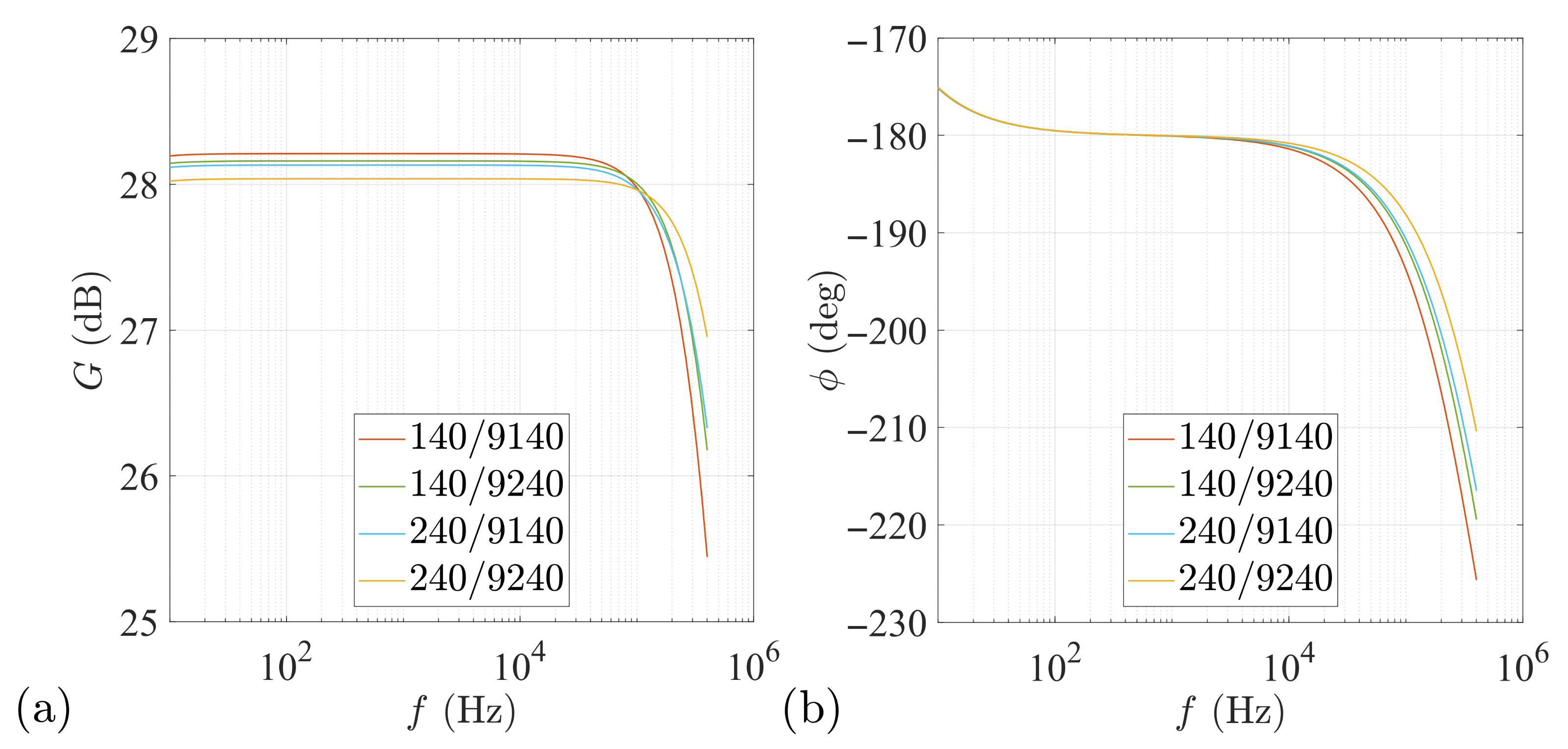
3.1. Numerical Simulation Issues: Simulation Results
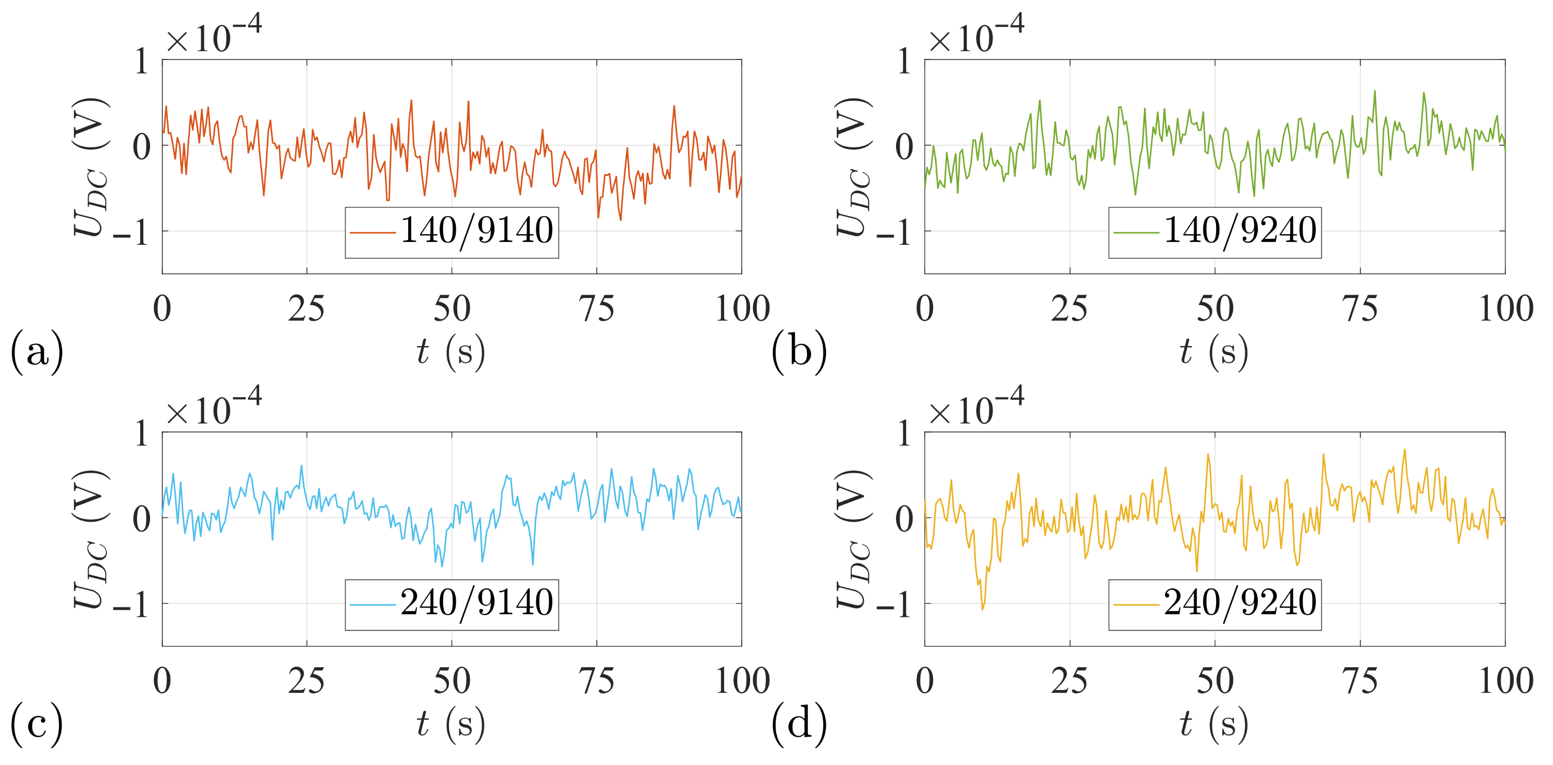
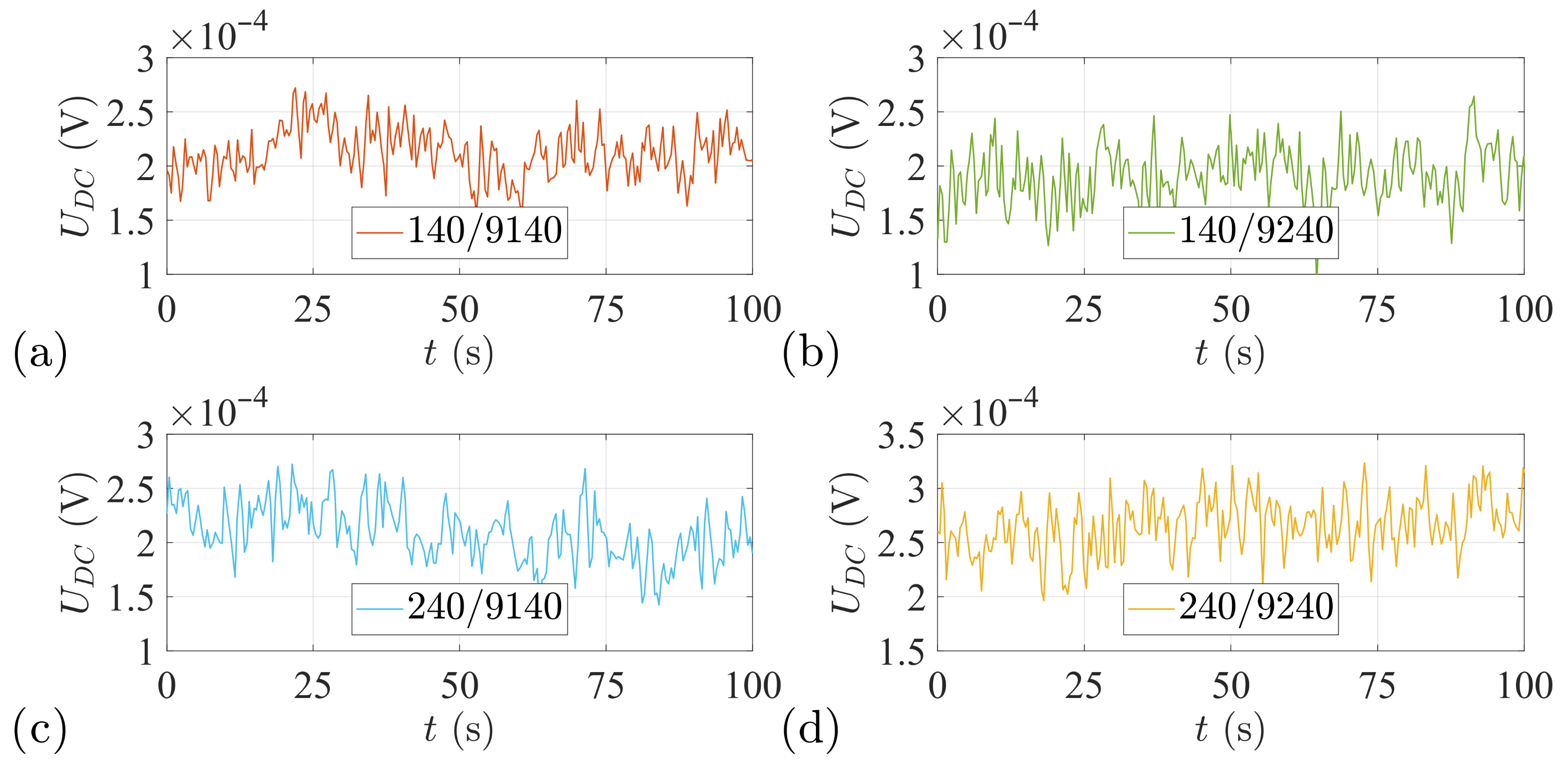
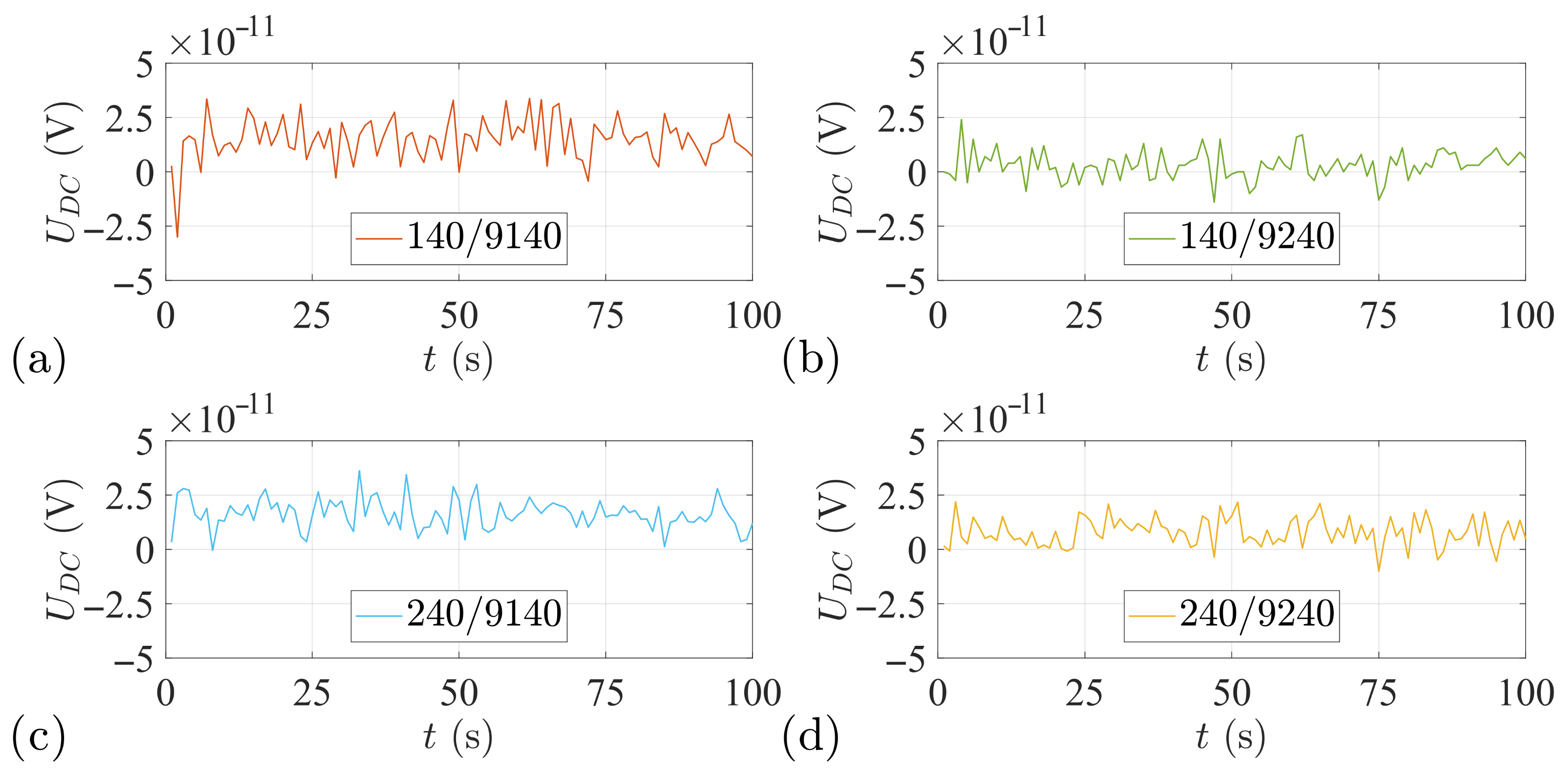
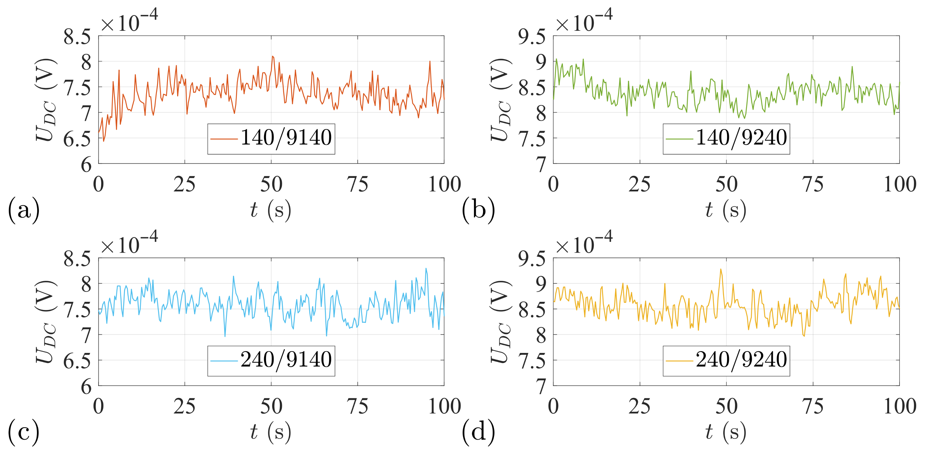
3.2. Real-World Device Tests
4. Conclusions
- Eliminating tube technology, which is subject to relatively rapid aging;
- Reduced power consumption owing to a significant reduction in supply voltage;
- Eliminating power supply filter chokes and thus simplifying the power supply system;
- Improved stability of electrical parameters by eliminating transformers that adapt the tube system to load or the next stage of the analog signal processing channel;
- Reducing heat emission, thus limiting the impact of high temperatures on the operation of other electronic components and adjacent function blocks;
- Significant simplification of system topology through improved operational indicators; and
- Significant reduction of the geometric and mass parameters of the device relative to the original tube system.
Author Contributions
Funding
Institutional Review Board Statement
Informed Consent Statement
Data Availability Statement
Conflicts of Interest
Appendix A

| No. | Label | Description | Parameters |
|---|---|---|---|
| 1. | R0 | load | n/a (8 for test purposes) |
| 2. | R1 | metallized resistor | 10 /3 W/5% |
| 3. | R2 | metallized resistor | 10 /3 W/5% |
| 4. | R3 | metallized resistor | 100 k/0.6 W/1% |
| 5. | R4 | metallized resistor | 100 k/0.6 W/1% |
| 6. | R5 | metallized resistor | 100 /0.6 W/1% |
| 7. | R6 | metallized resistor | 3.3 k/0.6 W/1% |
| 8. | R7 | metallized resistor | 260 /0.6 W/1% |
| 9. | R8 | metallized resistor | 100 k/0.6 W/1% |
| 10. | R9 | metallized resistor | 510 k/0.6 W/1% |
| 11. | R10 | metallized resistor | 5 k/0.6 W/1% |
| 12. | R11 | metallized resistor | 5 k/0.6 W/1% |
| 13. | R12 | metallized resistor | 1.5 k/1 W/5% |
| 14. | R13 | metallized resistor | 1.5 k/1 W/5% |
| 15. | R14 | metallized resistor | 100 k/0.6 W/1% |
| 16. | R15 | metallized resistor | 100 k/0.6 W/1% |
| 17. | R16 | metallized resistor | 270 /1 W/5% |
| 18. | R17 | metallized resistor | 100 /0.6 W/1% |
| 19. | R18 | metallized resistor | 100 /0.6 W/1% |
| 20. | R19 | metallized resistor | 270 /1 W/5% |
| 21. | R20 | ceramic resistor | 100 /5 W/5% |
| 22. | R21 | ceramic resistor | 100 /5 W/5% |
| 23. | R22 | metallized resistor | 330 /1 W/5% |
| 24. | R23 | metallized resistor | 330 /1 W/5% |
| 25. | R24 | ceramic resistor | 330 m/5 W/5% |
| 26. | R25 | ceramic resistor | 330 m/5 W/5% |
| 27. | R26 | ceramic resistor | 1 /10 W/5% |
| 28. | R27 | ceramic resistor | 1 /10 W/5% |
| 29. | POT1 | multi-turn assembly potentiometer | 10 k/0.5 W/10% |
| 30. | POT2 | multi-turn assembly potentiometer | 5 k/0.5 W/10% |
| 31. | C1 | electrolytic capacitor | 10,000 F/50 V |
| 32. | C2 | electrolytic capacitor | 10,000 F/50 V |
| 33. | C3 | electrolytic capacitor | 10,000 F/50 V |
| 34. | C4 | electrolytic capacitor | 10,000 F/50 V |
| 35. | C5 | polypropylene capacitor | 4.7 F/63 V/10% |
| 36. | C6 | ceramic capacitor | 33 pF/100 V/10% |
| 37. | C7 | polypropylene capacitor | 4.7 F/63 V/10% |
| 38. | C8 | polypropylene capacitor | 4.7 F/63 V/10% |
| 39. | C9 | electrolytic capacitor | 22,000 F/50 V |
| 40. | C10 | electrolytic capacitor | 22,000 F/50 V |
| 41. | C11 | electrolytic capacitor | 22,000 F/50 V |
| 42. | C12 | electrolytic capacitor | 22,000 F/50 V |
| 43. | OP1 | two-channel operational amplifier | NE5532AP |
| 44. | T1 | bipolar NPN transistor | BD139-16 |
| 45. | T2 | bipolar PNP transistor | BD140-16 |
| 46. | T3 | P-MOSFET transistor | IRFP9240 or IRFP9140 |
| 47. | T4 | N-MOSFET transistor | IRFP240 or IRFP140 |
| No. | Label | Description | Parameters |
|---|---|---|---|
| 1. | R14 | OMLT resistor | 750 k (750–820)/0.5 W/5% |
| 2. | R15 | OMLT resistor | 470 k/0.5 W/5% |
| 3. | R16 | OMLT resistor | 1.3 k/0.5 W/5% |
| 4. | R17 | OMLT resistor | 30 k/0.5 W/5% |
| 5. | R18 | linear potentiometer | 470 k/A/30% |
| 6. | R19 | OMLT resistor | 120 k/0.5 W/5% |
| 7. | R20 | OMLT resistor | 120 k/0.5 W/5% |
| 8. | R21 | OMLT resistor | 620 /0.5 W/5% |
| 9. | R22 | OMLT resistor | 15 k (12–20)/0.5 W/5% |
| 10. | R23 | OMLT resistor | 430 k/0.5 W/5% |
| 11. | R24 | OMLT resistor | 220 k/0.5 W/5% |
| 12. | R25 | OMLT resistor | 470 k/0.5 W/5% |
| 13. | R26 | OMLT resistor | 200 Ω/2 W/5% |
| 14. | R32 | MMT thermal resistor | 3 k/20% |
| 15. | C4 | MGBT capacitor | 47 nF/200 V/10% |
| 16. | C5 | MGBT capacitor | 47 nF/200 V/10% |
| 17. | C6 | MGBT capacitor | 47 nF/200 V/10% |
| 18. | C7 | MGBT capacitor | 47 nF/200 V/10% |
| 19. | C8 | MGBT capacitor | 2 F/160 V/10% |
| 20. | C13 | MGBT capacitor | 4 F/160 V/10% |
| 21. | C16 | KCOT capacitor | 360 pF (300–430)/250 V/5% |
| 22. | L2 | electron lamp | 6N2P-EW |
| 23. | L3 | electron lamp | 6N2P-EW |
| 24. | L4 | electron lamp | 6P1P-EW |
| 25. | L5 | electron lamp | 6P1P-EW |
| 26. | TR1 | transformer | n/a |
References
- Pietrasieński, J.; Rodzik, D.; Bużantowicz, W. The Tactical and Technical Functioning Conditions of the S-200C Vega Missile System on the Modern Battlefield. Saf. Def. 2021, 7, 80–89. [Google Scholar] [CrossRef]
- Koruba, Z.; Szmidt, P. The Remote Control of the Artillery Rocket Set as a Strongly Nonlinear System Subject to Random Loads. Electronics 2021, 10, 1507. [Google Scholar] [CrossRef]
- Pang, C.; Shan, G.; Ma, W.; Xu, G. Sensor radiation interception risk control in target tracking. Def. Technol. 2019, 16, 695–704. [Google Scholar] [CrossRef]
- Bużantowicz, W. Tuning of a Linear-Quadratic Stabilization System for an Anti-Aircraft Missile. Aerospace 2021, 8, 48. [Google Scholar] [CrossRef]
- Turinskyi, O.; Skoryk, A. Design method of surface-to-air missiles using the object-oriented approach and electronic launch technology. Sci. Technol. Air Force Ukr. 2019, 2, 133–142. [Google Scholar] [CrossRef]
- Pomohaiev, I.; Tarshyn, V.; Skoryk, A. Improved method of semi-active homing of surface-to-air missiles with measuring target-missile range. Sci. Technol. Air Force Ukr. 2020, 4, 95–101. [Google Scholar] [CrossRef]
- Gapiński, D.; Koruba, Z. Control of Optoelectronic Scanning and Tracking Seeker by Means the LQR Modified Method with the Input Signal Estimated Using of the Extended Kalman Filter. Energies 2021, 14, 3109. [Google Scholar] [CrossRef]
- Sinclair, I. Electronics Simplified, 3rd ed.; Elsevier: Kidlington, Oxford, UK, 2011. [Google Scholar] [CrossRef]
- Karapenev, B.D. Studies of Low-Frequency Power Amplifier Class D with Operational Amplifiers and Transistors. J. Electr. Electron. Eng. 2017, 5, 170–179. [Google Scholar] [CrossRef] [Green Version]
- Baliga, B.J. Silicon RF Power MOSFETs, 1st ed.; World Scientific: Singapore, 2005. [Google Scholar] [CrossRef]
- Ramella, C.; Piacibello, A.; Quaglia, R.; Camarchia, V.; Pirola, M. High Efficiency Power Amplifiers for Modern Mobile Communications: The Load-Modulation Approach. Electronics 2017, 6, 96. [Google Scholar] [CrossRef] [Green Version]
- Camarchia, V.; Quaglia, R.; Piacibello, A.; Nguyen, D.P.; Wang, H.; Pham, A.V. A Review of Technologies and Design Techniques of Millimeter-Wave Power Amplifiers. IEEE Trans. Microw. Theory Tech. 2020, 68, 2957–2983. [Google Scholar] [CrossRef]
- De Forest, L. The Audion: A New Receiver for Wireless Telegraphy. Trans. Am. Inst. Electr. Eng. 1906, 25, 735–763. [Google Scholar] [CrossRef]
- Kahng, D. Electric Field Controlled Semiconductor Device. US Patent No. 3,102,230, 27 August 1963. [Google Scholar]
- Atala, M.M. Semiconductor Devices Having Dielectric Coatings. US Patent No. 3,206,670, 14 September 1965. [Google Scholar]
- Ye, P.D.; Yang, B.; Ng, K.K.; Bude, J.; Wilk, G.D.; Halder, S.; Hwang, J.C.M. GaN MOS-HEMT using atomic layer deposition Al2O3 as gate dielectric and surface passivation. Int. J. High Speed Electron. Syst. 2004, 14, 791–796. [Google Scholar] [CrossRef]
- Mimura, T. Development of High Electron Mobility Transistor. Jpn. J. Appl. Phys. 2005, 44, 8263–8268. [Google Scholar] [CrossRef]
- Lee, S.H.; Lim, J.W.; Kang, D.M.; Baek, Y.S. Technical Trends in Next-Generation GaN RF Power Devices and Integrated Circuits. Electron. Telecommun. Trends 2019, 34, 71–80. [Google Scholar] [CrossRef]
- Pearton, S.J.; Ren, F.; Tadjer, M.; Kim, J. Perspective: Ga2O3 for ultra-high power rectifiers and MOSFETS. J. Appl. Phys. 2018, 124, 220901. [Google Scholar] [CrossRef] [Green Version]
- Fujiwara, S.; Yamamoto, K.; Miyashita, M.; Yamabe, S.; Kabayashi, D. Power Amplifier. US Patent No. US 9,041,473 B2, 26 May 2015. [Google Scholar]
- Grebennikov, A. RF and Microwave Power Amplifier Design, 2nd ed.; McGraw Hill: New York, NY, USA, 2015. [Google Scholar]
- Lewis, G.K.; Olbricht, W.L. Development of a portable therapeutic and high intensity ultrasound system for military, medical, and research use. Rev. Sci. Instrum. 2008, 79, 114302. [Google Scholar] [CrossRef] [PubMed]
- Golub, G.H.; Van Loan, C.F. Matrix Computations, 3rd ed.; Johns Hopkins: Baltimore, MD, USA, 1996. [Google Scholar]
- Mulya, M.A.J.; Alam, B.R. Design of Low Noise Amplifier of a Broadband RF IC Transponder for RF Link in Manufacture 4.0. In Proceedings of the 2019 International Symposium on Electronics and Smart Devices (ISESD), Bali, Indonesia, 8–9 October 2019; pp. 1–4. [Google Scholar] [CrossRef]
- Borys, S.; Kaczmarek, W.; Laskowski, D. Selection and Optimization of the Parameters of the Robotized Packaging Process of One Type of Product. Sensors 2020, 20, 5378. [Google Scholar] [CrossRef] [PubMed]


| Parameter | Value |
|---|---|
| amplifier bandwidth | from 20 Hz to 20 kHz |
| output signal power | ≥10 W |
| distortion product ratio | <1% |
| DC level of output signal | <2.5 mV |
| height × length × width (incl. mounting platform) | 120 × 210 × 300 mm |
| mass of the amplifier module (incl. frames and covers) | <5 kg |
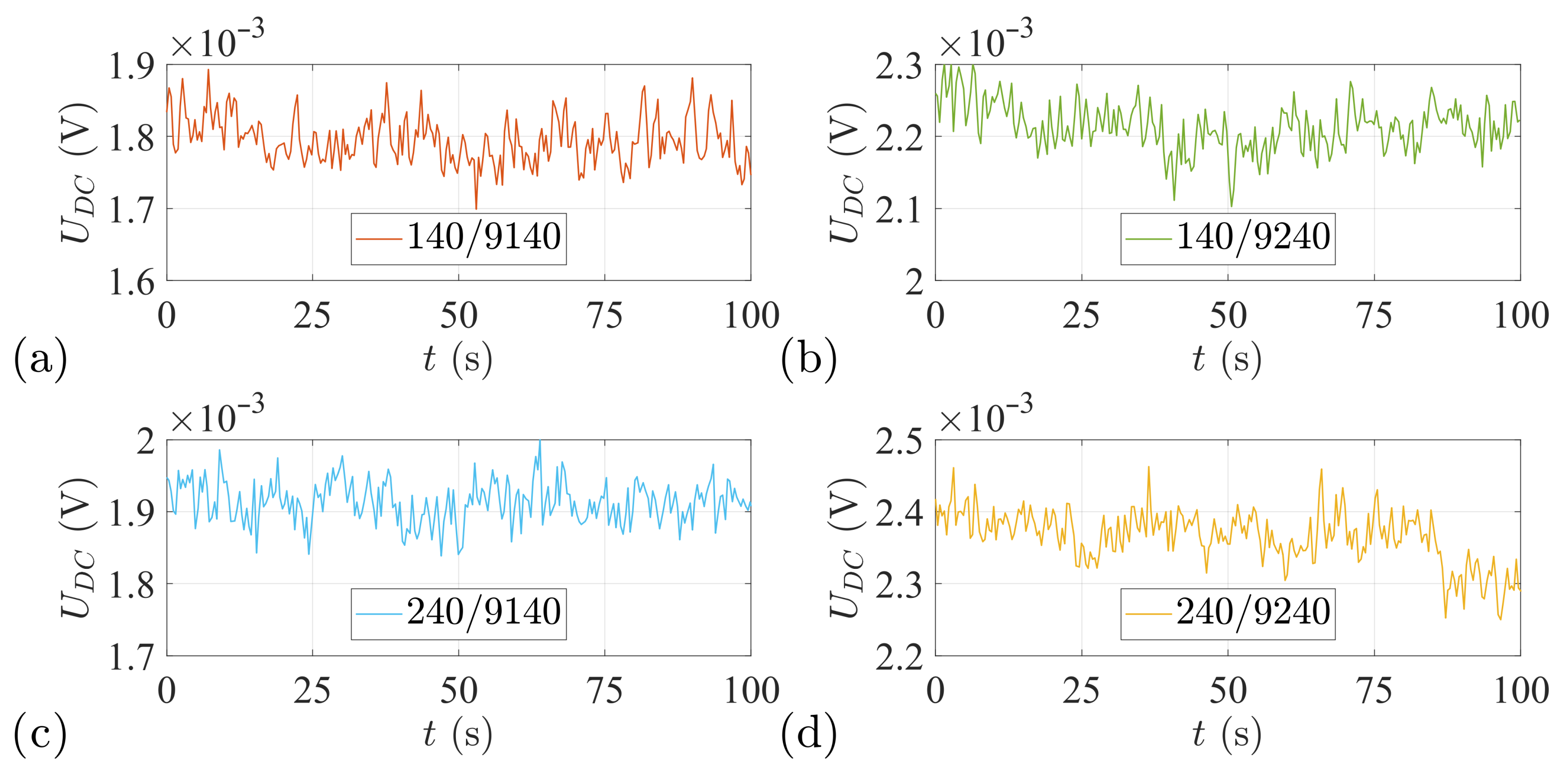
| Parameter of | 140/9140 | 140/9240 | 240/9140 | 240/9240 |
|---|---|---|---|---|
| mean value (V) | ||||
| standard deviation (V) |
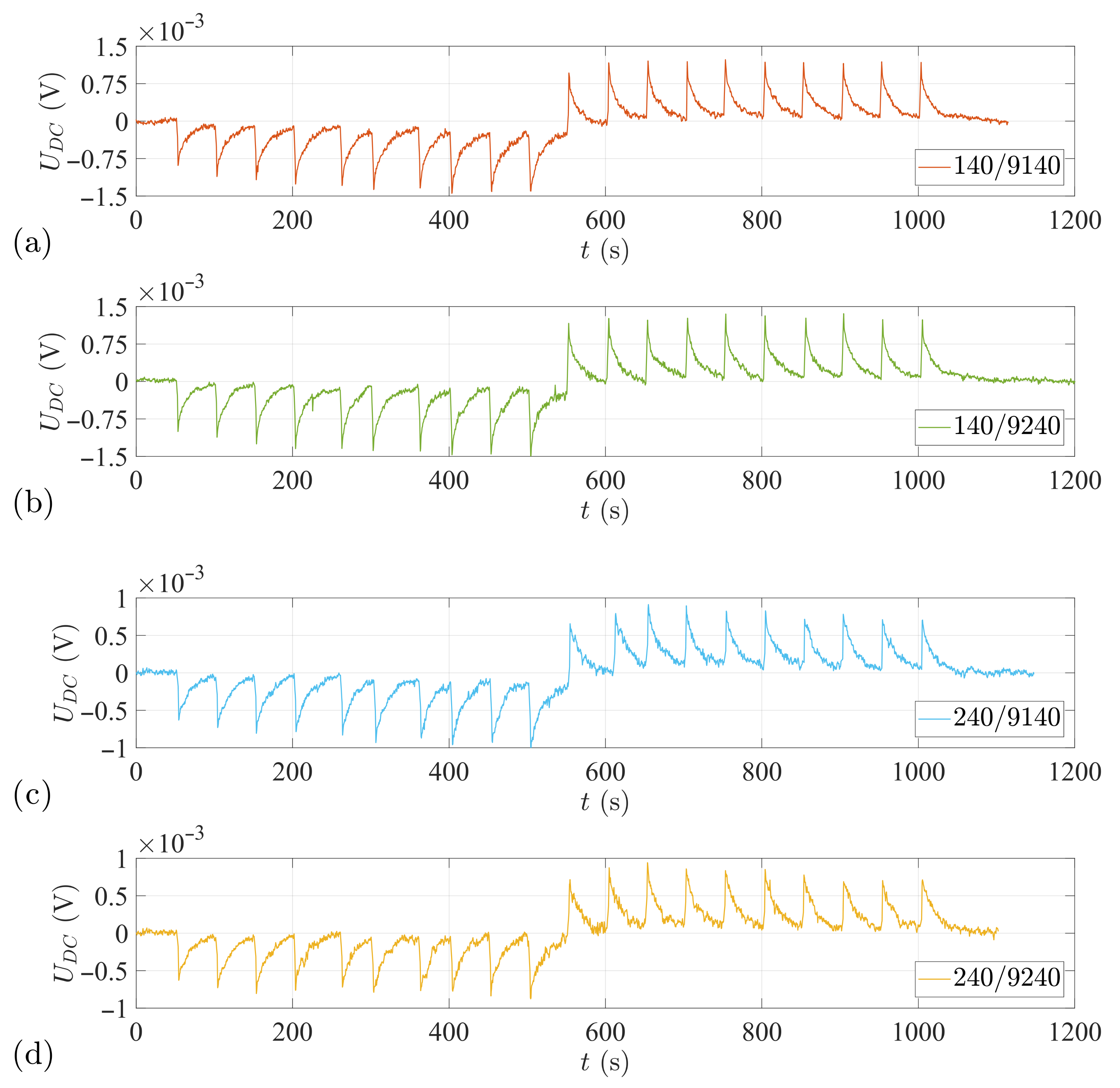
| Parameter of | 140/9140 | 140/9240 | 240/9140 | 240/9240 |
|---|---|---|---|---|
| mean value (V) | ||||
| standard deviation (V) |
Publisher’s Note: MDPI stays neutral with regard to jurisdictional claims in published maps and institutional affiliations. |
© 2022 by the authors. Licensee MDPI, Basel, Switzerland. This article is an open access article distributed under the terms and conditions of the Creative Commons Attribution (CC BY) license (https://creativecommons.org/licenses/by/4.0/).
Share and Cite
Żółtowski, P.; Bużantowicz, W. Self-Balancing Power Amplifier with a Minimal DC Offset for Launcher Automation Control Circuits of a Surface-to-Air Missile System. Appl. Sci. 2022, 12, 3532. https://doi.org/10.3390/app12073532
Żółtowski P, Bużantowicz W. Self-Balancing Power Amplifier with a Minimal DC Offset for Launcher Automation Control Circuits of a Surface-to-Air Missile System. Applied Sciences. 2022; 12(7):3532. https://doi.org/10.3390/app12073532
Chicago/Turabian StyleŻółtowski, Piotr, and Witold Bużantowicz. 2022. "Self-Balancing Power Amplifier with a Minimal DC Offset for Launcher Automation Control Circuits of a Surface-to-Air Missile System" Applied Sciences 12, no. 7: 3532. https://doi.org/10.3390/app12073532
APA StyleŻółtowski, P., & Bużantowicz, W. (2022). Self-Balancing Power Amplifier with a Minimal DC Offset for Launcher Automation Control Circuits of a Surface-to-Air Missile System. Applied Sciences, 12(7), 3532. https://doi.org/10.3390/app12073532