Article

Self-Balancing Power Amplifier with a Minimal DC Offset for Launcher Automation Control Circuits of a Surface-to-Air Missile System

by
Piotr Żółtowski
and
Witold Bużantowicz
*
Faculty of Mechatronics, Armament and Aerospace, Military University of Technology, Gen. S. Kaliskiego 2 Street, 00-908 Warsaw, Poland
*
Author to whom correspondence should be addressed.
Appl. Sci. 2022, 12(7), 3532; https://doi.org/10.3390/app12073532
Submission received: 14 February 2022 / Revised: 24 March 2022 / Accepted: 28 March 2022 / Published: 30 March 2022
(This article belongs to the Special Issue Automation Control and Robotics in Human-Machine Cooperation)

Abstract

:
This paper discusses the design of a new self-balancing amplifier of an AC component power characterized by a minimal output DC offset. The design of the amplifier is based on semiconductor technology and intended for application in low-frequency analog signal processing paths, particularly in surface-to-air missile system launcher automation circuits. The proposed solution has several design and technical-implementation advantages, whereas the primary novelty compared to the commonly used ones is the ability for self-generating a near-zero DC component value of output signal. The design features and technical parameters of the developed amplifier make it suitable for use in a wide range of devices that must ensure the stable, prolonged operation of a low-frequency power amplifier under variable weather conditions and a minimal DC offset of output signal.

1. Introduction

Surface-to-air missile systems are specific engineering products. In terms of their design, they are the progenitors of advanced mechatronic systems. They are characterized by the technical diversity of their elements, functional complexity, advanced signal processing from air targets and missiles, and high levels of automation and operating precision, often under unfavorable conditions of enemy counteractions. Their scientific and technical interdisciplinarity, which combines many complex issues in the fields of mechanics, material engineering, chemistry, radio electronics, and information technology as well as the need to adapt to extreme battlefield conditions, makes surface-to-air missile systems extremely expensive to develop and manufacture, and their introduction to armament has repercussions for several dozen years [1]. On the other hand, scientific and technical progress makes it impossible to ensure technical modernity over such a long period.
This mainly applies to medium- and long-range surface-to-air missile systems, which are among the most complex armament types. A systematic increase in the combat capabilities of air attack and changes in air strike tactics has given rise to a need for the continuous adaptation of anti-aircraft systems [1,2,3] and missiles [4,5,6,7] to contemporary air combat requirements. In particular, this applies to older-generation systems designed for different conditions of use [1].
One primary direction of modernization involves projects associated with modernizing electronic systems in the processing paths for analog and digital signals, particularly processing radar signals from air targets and missiles, mapping air situations, generating control signals in missile launch control systems, and generating missile launch commands and transmitting them via the radio channel. This modernization will develop completely new solutions aimed at increasing the fire efficiency of a system and significantly improving its operational and economic properties. This is why it is important for the systems to ensure a generational change in the performance quality of a missile system without disturbing the structure of its instrumentation. For obvious reasons, this paper will address only a narrow aspect of modernizing a surface-to-air missile system. We considered issues related to replacing one of the launcher automation module tube amplifier circuits with a circuit that covers a power amplifier constructed with semiconductor technology.
In general, power amplifiers supply the required output power with minimum distortions within the assumed operating bandwidth [8]. The frequency band of processed signals enables a division into (a) low-frequency (LF) power amplifiers for boosting low-frequency signals; (b) high-frequency (HF) power amplifiers for amplifying radio band signals; and (c) very high-frequency (VHF) power amplifiers used on microwave signal processing paths [9,10,11,12]. Power amplifiers first appeared in the 1910s as a consequence of the invention of triodes [13]. Vacuum tubes had been the basis for amplifier construction until the second half of the previous century. Their widespread use in older-generation missile system instrumentation dated back to the 1950s. The development of transistors in the middle of the 1950s and their popularization prompted the gradual transition from tube systems to ones that used semiconductor technology, including military technology. Metal–oxide–semiconductor field-effect transistors (MOSFETs) are particularly interesting in this context. They are characterized by very high input impedance and low output impedance [14,15]. They can be used autonomously or in pairs with bipolar junction transistors (BJT) within LF and HF amplifier structures [10]. Despite the gradual popularization of systems based on contemporary solutions, e.g., power amplifiers constructed with GaN, GaAs, Ga 2 O 3 or SiC technologies [11,12,16,17,18,19], amplifiers with classic MOSFET transistors are still being developed and widely used in typical applications within civilian and military technology due to their properties, availability, and price [19,20,21,22].
This paper presents a design of a new self-balancing amplifier of an AC component power characterized by a minimum DC offset of output signal. The amplifier is based on a semiconductor technology intended for application in LF analog signal processing paths, especially in anti-aircraft missile system launcher automation circuits. The proposed system has several design and technical-implementation advantages, whereas the primary novelty compared to commonly used solutions is the ability for self-generating a near-zero DC component value of output signal.
The paper is organized as follows. Section 2.1 presents a formal approach to the issue and preliminary power amplifier project assumptions. Section 2.2 and Section 2.3 offer a detailed description of the system’s topology, hardware implementation, and principle of operation. Section 3 discusses the results of simulation and real device tests. Section 4 concludes the paper with a summary and final remarks.

2. Materials and Methods

2.1. Problem Formulation: Initial Design Assumptions

Figure 1 shows a diagram of a tube amplifier intended for replacement. The device is a typical push–pull LF system based on LF triodes, L2 and L3, and LF power tetrodes, L4 and L5. Appendix A includes a tabular list and description of elements comprising the circuit. The system is part of one of the electronic modules within the considered anti-aircraft missile launcher (Figure 2), and its task is to generate a radio fuse trigger angle setting signal depending on the velocity of the missile approaching an air target.
The phase inverter system is crucial for this issue. In general, a phase inverter should be characterized by minimum output signal distortions, a wide frequency bandwidth, and high output signal symmetry, which is required to correctly control the LF power output tubes. In this case, the phase inverter stage is based on two LF triodes, L3A and L3B, placed in a single glass bulb of electron tube L3. Resistors R19–R21 determine the operating conditions of lamp L3 for a DC component stage. Elements R22–R25 and capacitors C6, C7, and C16 affect the system operating conditions for the AC component. Introducing local feedback for the AC component implements an input signal phase inverter system. Output signal symmetry is determined by the value of resistor R22. Elements C6 and C7 separate the phase inverter stage from the power stage of the DC component. The power stage design is based on lamps L4 and L5, resistor R26, and transformer TR1, which adjusts the high output impedance of the lamps to the low load impedance of this stage.
Capacitor C8 limits the amplifier bandwidth. Capacitor C13 is the last anode voltage power supply filter capacitor. Half of electron tube L2, together with auxiliary elements (resistors R14–R17, thermistor R32, and capacitors C4–C5), implements the voltage amplifier stage supplying an adequate level of control voltage to the phase inverter system.
An undoubted advantage of this LF amplifier system is the high amplification of the output signal. Its downside is its high sensitivity to clipping. A significant limitation is the fact that input signal source voltage should not exceed the L2 tube grid polarization voltage, since exceeding this value translates to a significant increase in distortions on the amplifier output. It should be emphasized that triode L3 may age unevenly, which will lead to increased nonlinear distortions (loss of balance) over time. Another significant operational limitation is high heat emission because of the considerable impact of temperature on the operation of other electronic components and adjacent functional blocks, implying a need to use cooling systems. Please also note that tube systems require additional filament circuits for lamps L2–L5. They should be filament voltage power supply systems, which demand more power.
Consequently, we proposed replacing this LF tube amplifier system with an innovative system using semiconductor technology. The main tasks of the newly designed LF power amplifier include (a) generating an LF output signal with specified parameters over the entire range of assumed processing band; (b) generating a minimum signal DC component level at the output (load) regardless of instantaneous unbalanced supply voltage fluctuations; and (c) possibly ensuring the lowest distortion product ratio (DPR) level while maintaining a high signal-to-noise (SNR) ratio. Table 1 lists the assumed structural parameters of the system.
The amplifier must spontaneously balance the output DC component value at a near-zero level during prolonged operation and when controlling through an LF analog signal (i.e., active operation). Furthermore, it is assumed that this functionality will be obtained without applying additional elements within the LF channel, which would separate the DC component from load in the form of LF transformers or blocking capacitors. This is induced by the desire to limit the presence of inductive and capacitive elements that significantly affect harmonic distortions, frequency bandwidth, and output signal phase.
The objective is to ensure stable and continuous system operation, independent of instantaneous fluctuations of unbalanced supply voltage and unfavorable operating conditions (especially in the event of sudden changes in ambient temperature).

2.2. Circuit Design

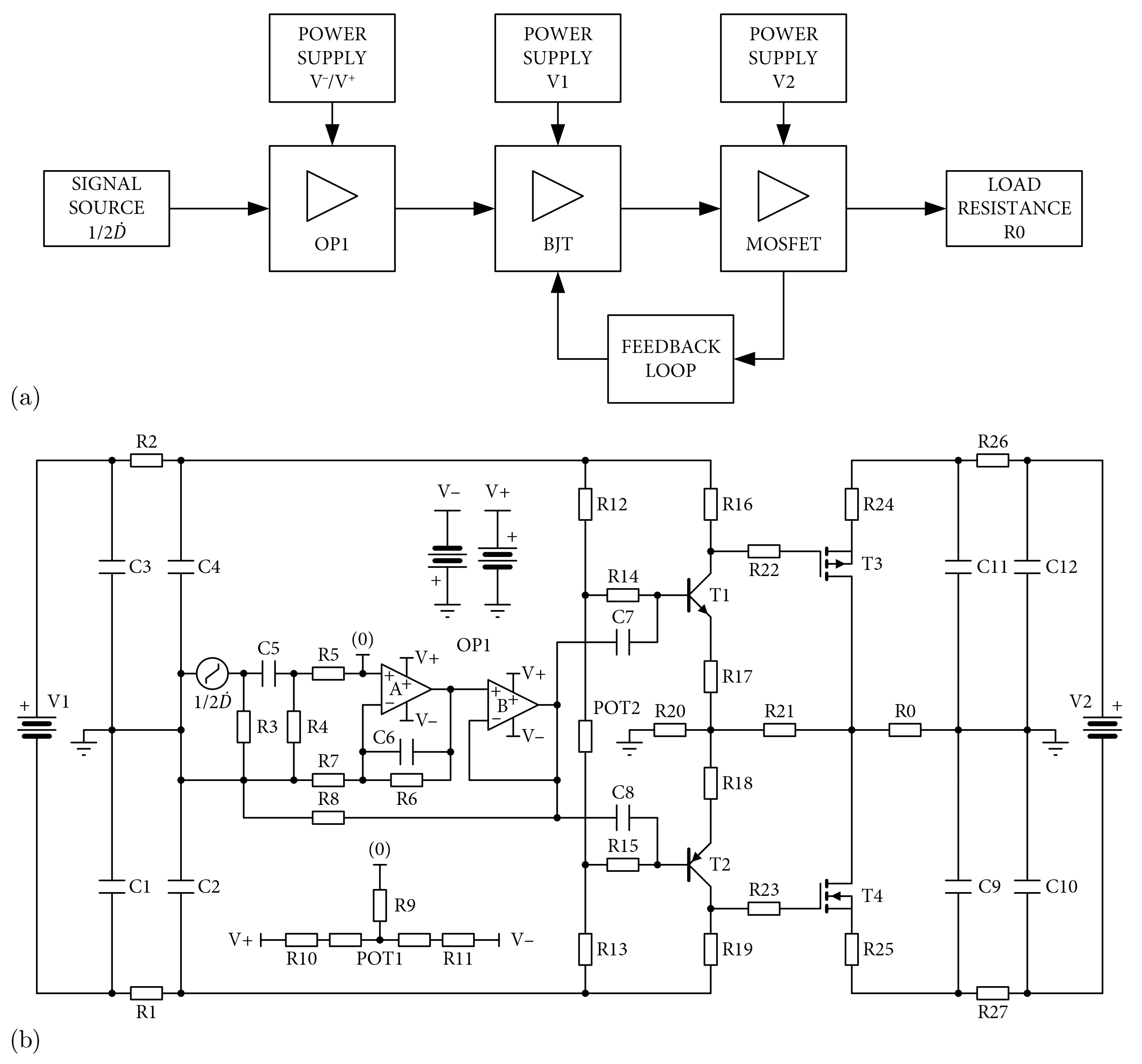
The proposed device is a symmetric, three-stage LF amplifier system (Figure 3a). A diagram of the designed amplifier is shown in Figure 3b. Appendix A includes a tabular list and description of the elements comprising the circuit.
The first (input) stage consists of operational amplifiers OP1A and OP1B and resistance elements from R3 to R11. The OP1A amplifier is a voltage amplifier. Its voltage gain in the negative feedback loop is determined through resistors R6 to R7. Amplifier OP1B acts as a voltage follower that reduces the first-stage output impedance.
The control voltage from signal source 1/2 D ˙ is directed to the non-inverting input of the amplifier OP1A through the separating capacitor C5. The latter has two functions. First, it protects the OP1A amplifier channel against the unwanted appearance of a DC component, which may appear at the output of source 1/2 D ˙ (by definition, the amplifier is not a DC component amplifier). Second, it separates the source of signal 1/2 D ˙ from the side of amplifier OP1A through the application of a system of resistors R9–R11 and POT1, which compensates for the output DC component of the OP1A and OP1B amplifiers. The ceramic capacitor C6 protects OP1A against excitation, limiting the OP1 bandwidth.
The second stage (LF voltage follower) is based on bipolar transistors T1 and T2. Elements R12, POT2, and R13 form a voltage divider that polarizes the bases of transistors T1 and T2 while simultaneously determining the DC operating conditions. Resistors R14 and R15 separate the low impedance of the polarization divider from bases of transistors T1 and T2 while improving system parameters in terms of low frequencies. Elements C7 and C8 act as capacitors coupling the first amplifier stage with the second one for the AC component while simultaneously separating these stages in terms of their DC component.
The third (end) stage was constructed using T3 and T4 transistors that employ MOSFET technology. Resistor R0 has a load function within the system. The current of collectors T1 and T2 flowing through R16 and R19 polarizes end-stage transistor gates, thus impacting the opening voltage for gates T3 and T4, which leads to determining the operating conditions for this stage of the DC component.
The amplifier’s operation is protected by three independent DC power circuits. The first stage is supplied with stabilized balanced voltage of ±15 V. The second stage is supplied with V1 unbalanced voltage, which, after passing symmetrical low-pass filters of the π type (elements R1, C1, C2, and R2, C3, C4), forms a balanced power supply system. Similarly, the third stage is supplied with a balanced system that supplies unbalanced V2 voltage to symmetrical low-pass filters of the π type (elements R26, C11, C12, and R27, C9, C10).
The application of independent DC power of the voltage follower stage (T1 and T2) and power followers T3 and T4 (the so-called power output stage) is a particular and crucial solution within the amplifier. Separating the stages due to power supply is necessary to generate and obtain minimum unbalanced voltage of the amplifier at a near-zero level, with load resistance and associated with voltage self-balancing of the amplifier at its output under conditions of continuous and uninterrupted operation. Such a power supply method simultaneously ensures proper DC output power operating conditions and facilitates independent and stable stage operation, which is particularly important for the T3 and T4 transformers. This creates operating conditions for the output voltage DC component, which in turn obtains a minimum offset voltage value and maintains such a state with and without setting the 1/2 D ˙ input signal. In a classic approach, the amplifier is powered by symmetrical voltage; however, this does not give satisfactory results in time-varying conditions. Here, conversely, the application of an unbalanced DC power supply source facilitates maintaining a minimum level of output DC component through a power follower without affecting the preceding stage. Both stages, together with low-pass symmetrical filter assemblies, spontaneously (independently of each other) develop symmetrical DC power supply values that are convenient for the required DC operating conditions.
Covering the second and third amplifier stages with a feedback loop additionally contributes to obtaining the minimum offset voltage value. Furthermore, it impacts the DC operating conditions of the stages covered by the feedback, limiting their gain values by approximately two times (gain is determined with the R20/R21 resistance ratio).

2.3. Hardware Implementation

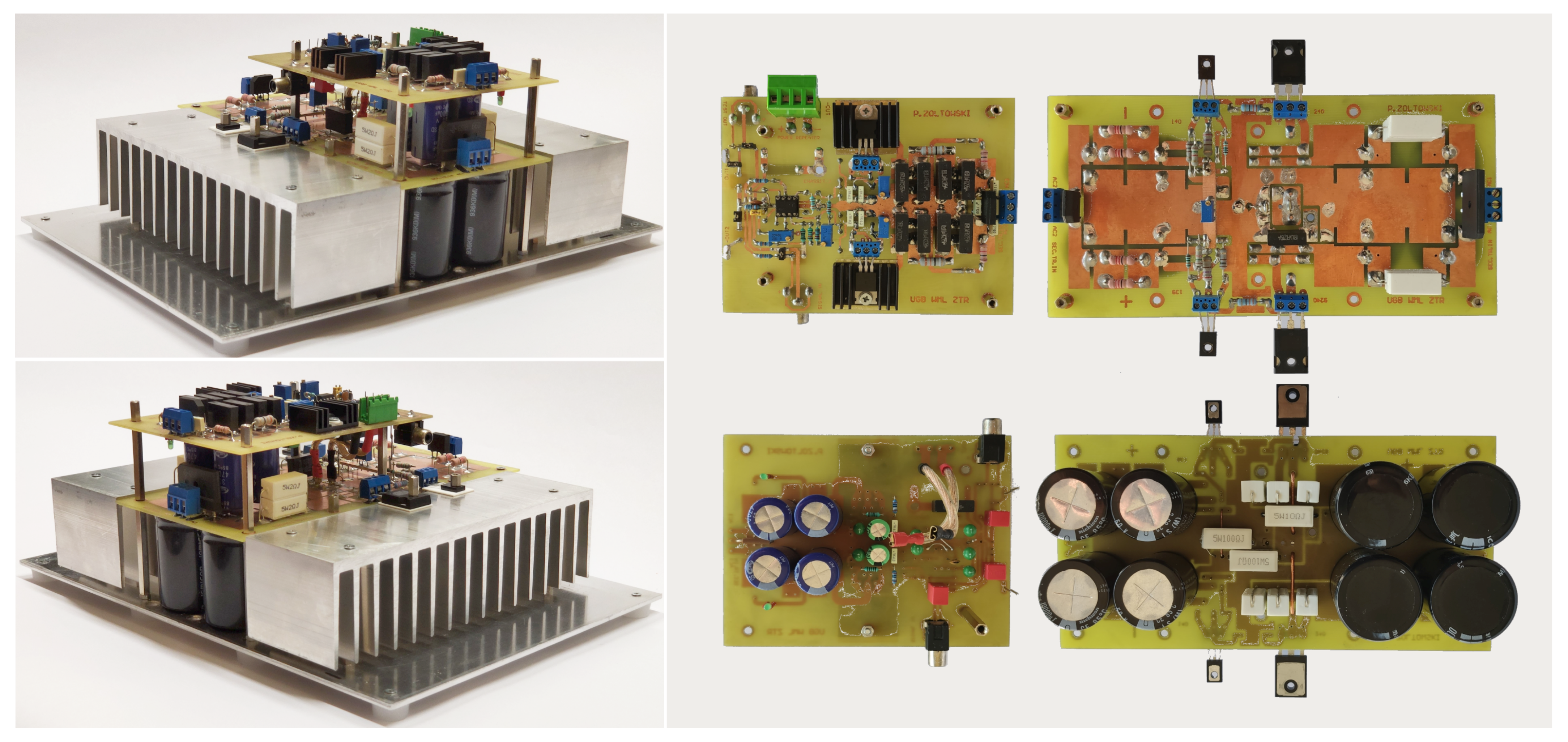
Due to electro-mechanical functionality, the hardware implementation of this LF amplifier is characterized by modularity and structural symmetry. We paid particular attention to ensuring convenient access to electronic components and to the appropriate assembly of semiconductor elements that are responsible for dissipating excess heat. The device was intentionally built using industrial nonlinear, active components—i.e., components that are not used in commercial, specialized solutions for LF power signal processing. The complete amplifier module (including mounting platform and heat sinks) measures 115 × 210 × 300 mm and weighs just under 2.5 kg (Figure 4). The power consumption of the device is less than 30 W for 10 W of output power at the load resistance.
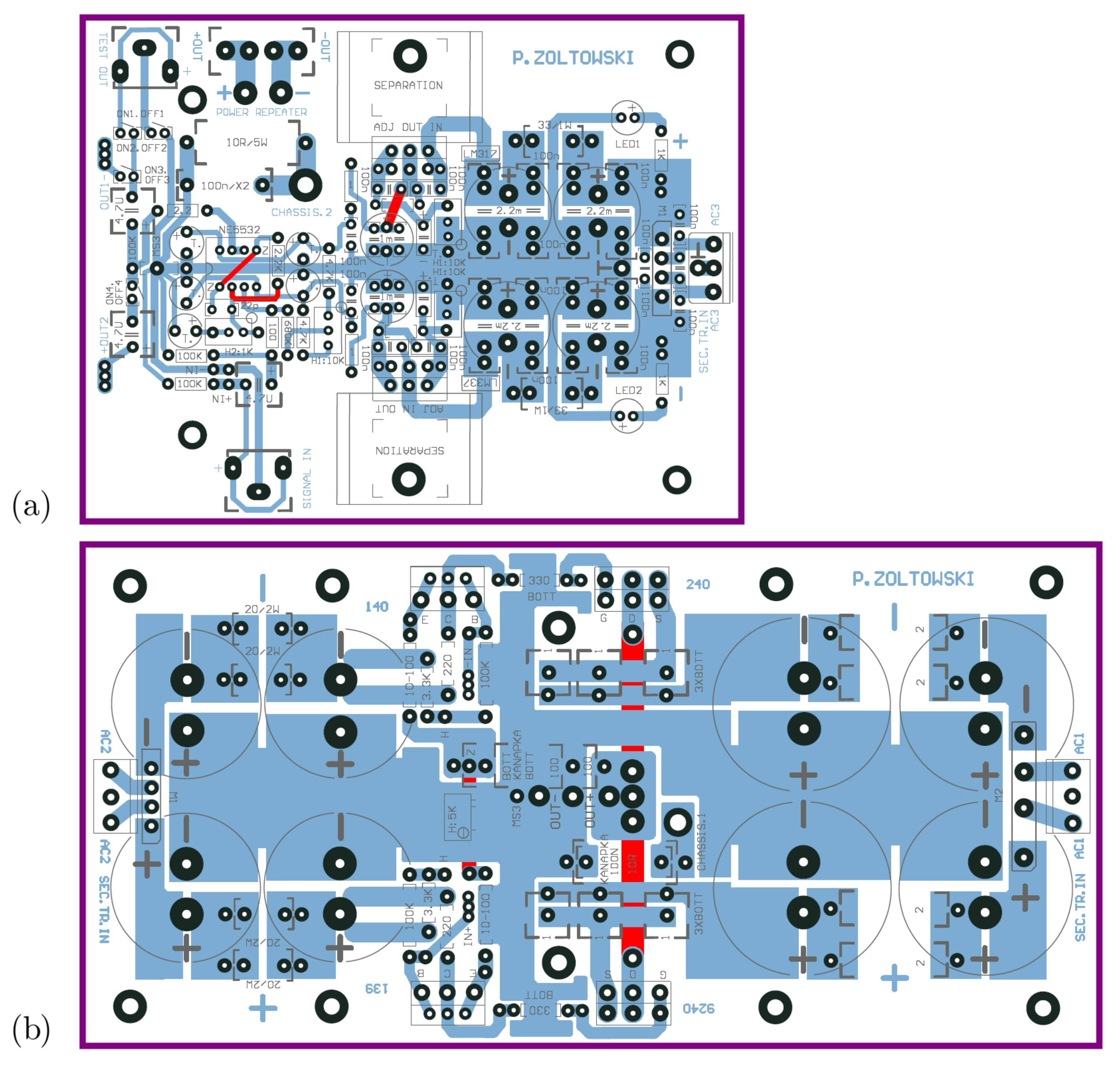
The PCB of the 1/2 D ˙ input signal system with a two-channel operational amplifier NE5532AP measures 130 × 102 mm (cf. Figure 5a). It is not integrated with the device’s motherboard. It is fixed over a part of the power follower using metal mounting pins. The board has a classic ±15 V power supply based on voltage stabilizers LM317 and LM337. To ensure a high level of stability of the OP1 supply voltage, LM-type voltage stabilizers were used, which were equipped with local heat sinks to remove excess heat from their surfaces. Electronic elements have been arranged to ensure (a) the possibly shortest signal paths for the 1/2 D ˙ signal to the operational amplifier input and output; and (b) routing a processed signal to a subsequent amplifier voltage follower stage, i.e., bases of bipolar transistors T1 and T2 located on the motherboard. At the same time, convenient access to the quiescent current adjustment potentiometer of the MOSFET transformer pair (T3 and T4) was ensured.
The device’s motherboard (Figure 5b) measures 130 × 211 mm. The motherboard covers the voltage follower system, power follower system, and supply voltage filtering elements of these stages. It is fixed using metal assembly pins to a chassis between radiators that dissipate heat from active elements. The motherboard path mosaic has been designed so the 1/2 D ˙ signal ground of the preamplifier stage is connected at one point with the ground of the motherboard power supply system and the grounds of the power supplies for the operational amplifier, voltage follower, and power follower. A common ground point is connected to the mechanical structure chassis.

3. Results and Discussion

This section presents the results of simulation (Section 3.1) and real-world (Section 3.2) tests of the LF amplifier circuit as designed. In addition, these sections include observations and comments relating directly to the results of the tests.

3.1. Numerical Simulation Issues: Simulation Results

As a result of formal limitations, an analytical solution to nonlinear state equations is not generally possible, so system operation was analyzed using numerical methods. Conservative elements making up the system were replaced with associated models, which enabled transforming dynamic systems in corresponding DC systems for a single sampling step. Equations formulated using a modified balance nodal method, given in general form
GV = I
where G R n × n is the system conductance matrix, V R n × 1 is the sought nodal potential vector, and I R n × 1 is the excitation (current) vector, were solved by combining the lower–upper decomposition (LU) method with the sparse matrix technique, which avoided the consideration of trivial cases [23].
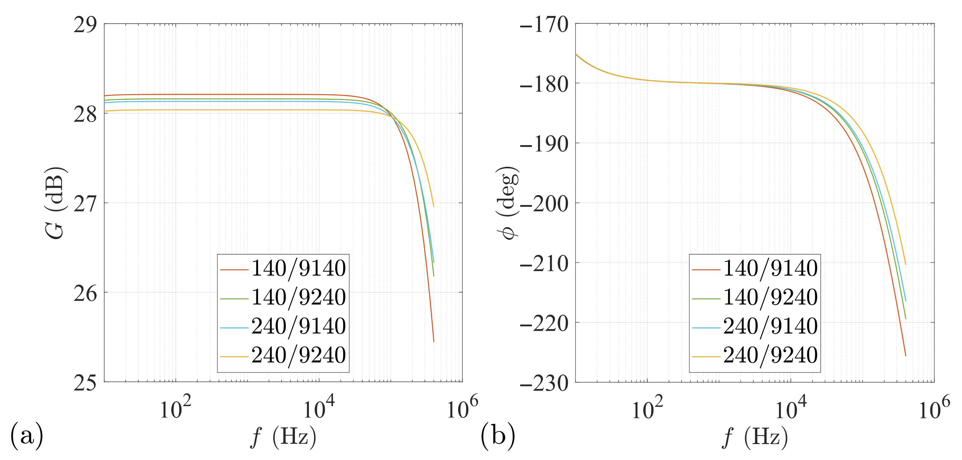
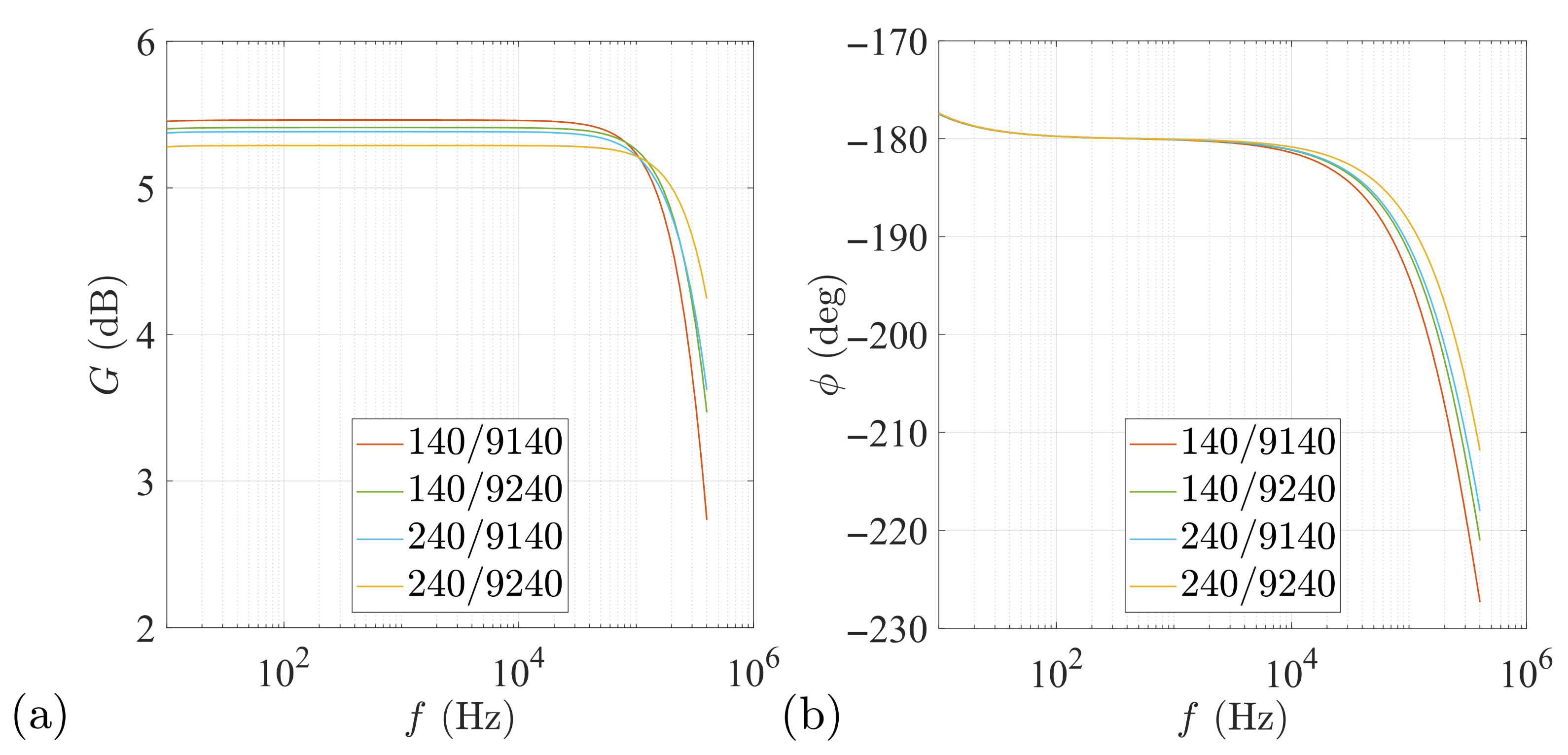
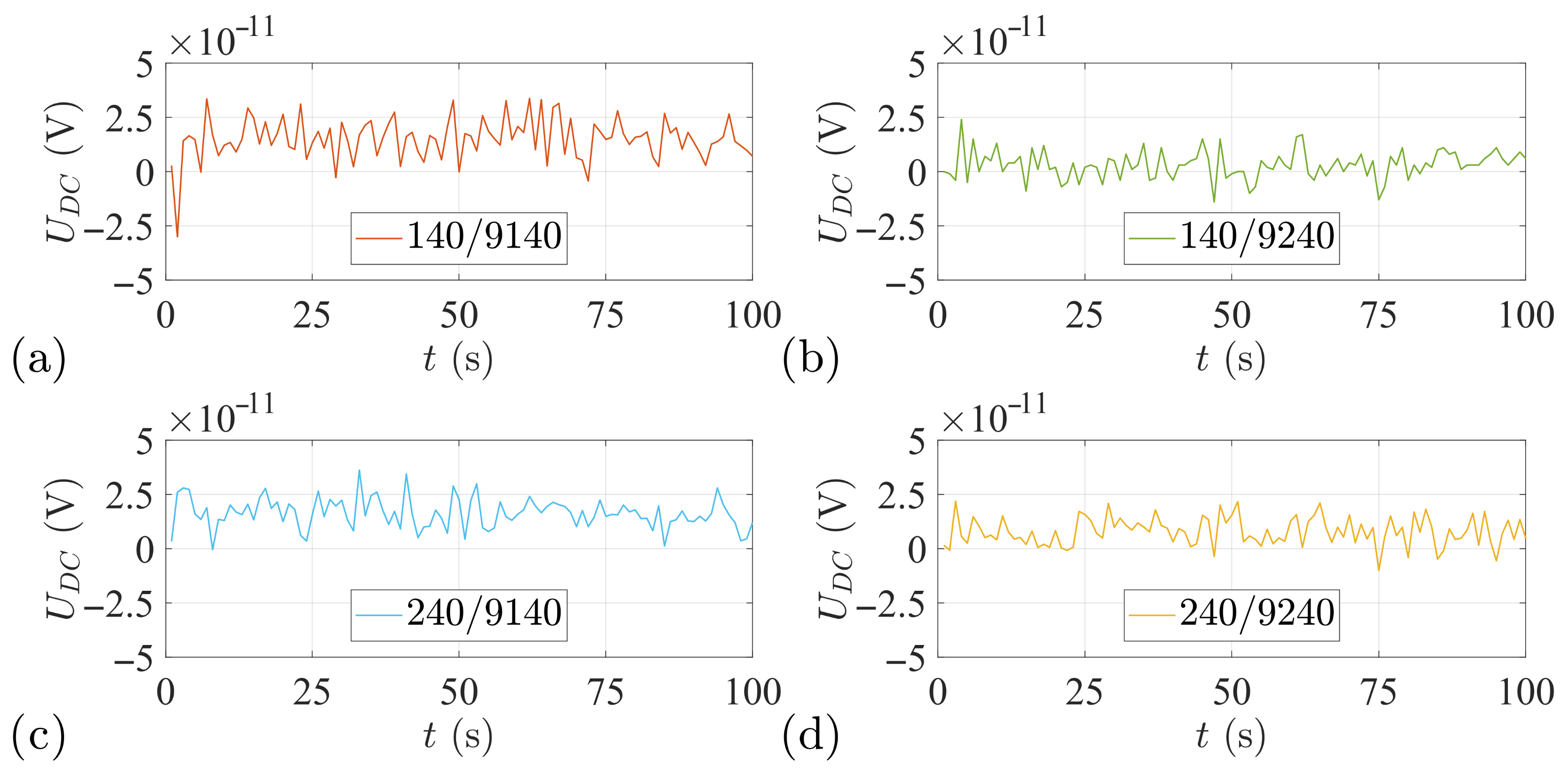
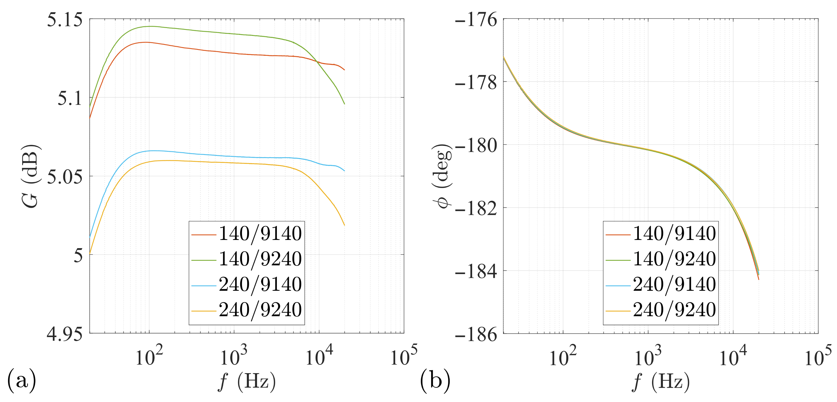
Selected results from the computer simulation are shown in Figure 6, Figure 7 and Figure 8. Figure 6 and Figure 7 show the amplitude-phase characteristics of the amplifier for the four configurations of the transistor pairs used: IRFP140/IRFP9140 and IRFP240/IRFP9240. These four transistor pairs were used to show that the DC level value at output does not depend on used semiconductor active elements. Figure 6 illustrates the results obtained from the simulation for the designed circuit with an OP1A preamplifier attached, while Figure 7 depicts it without the preamplifier. In both cases, the amplifier is designed to have a uniform signal gain in the frequency band in question (up to 10 4 Hz): approximately 28 dB for the system with the pre-processing stage attached (Figure 6a) and approximately 5 dB for the system without the OP1A amplifier (Figure 7a). The circuit inverts the phase of the input signal (Figure 6b and Figure 7b) and has favorable phase characteristics (no undesirable shifts). Since the OP1A preamplifier does not cause any significant changes in the circuit’s operation (apart from the gain value), it was excluded from further considerations. Figure 8 shows the results of the simulation for the DC component voltage U D C on the system load for the tested pairs of transistors, with input capacitors C7 and C8 shorted to ground. The voltage U D C measured at the output of the system was very low (on the order of tens of pV) and did not undergo rapid changes over time. The mean values of these voltages and their standard deviations for each transistor pair are shown in Table 2.

3.2. Real-World Device Tests

The physically constructed LF amplifier was tested under laboratory conditions. The tests were carried out using an AudioPrecision AP x525 multifunctional measuring and testing system, which is designed to assess the operation of signal processing equipment in the LF domain.
Figure 9 and Figure 10 present the measurements of basic device parameters. The results are presented for individual pairs of power transistors, which allows us to demonstrate the universality of the solution and its resistance to changing operating or production conditions.
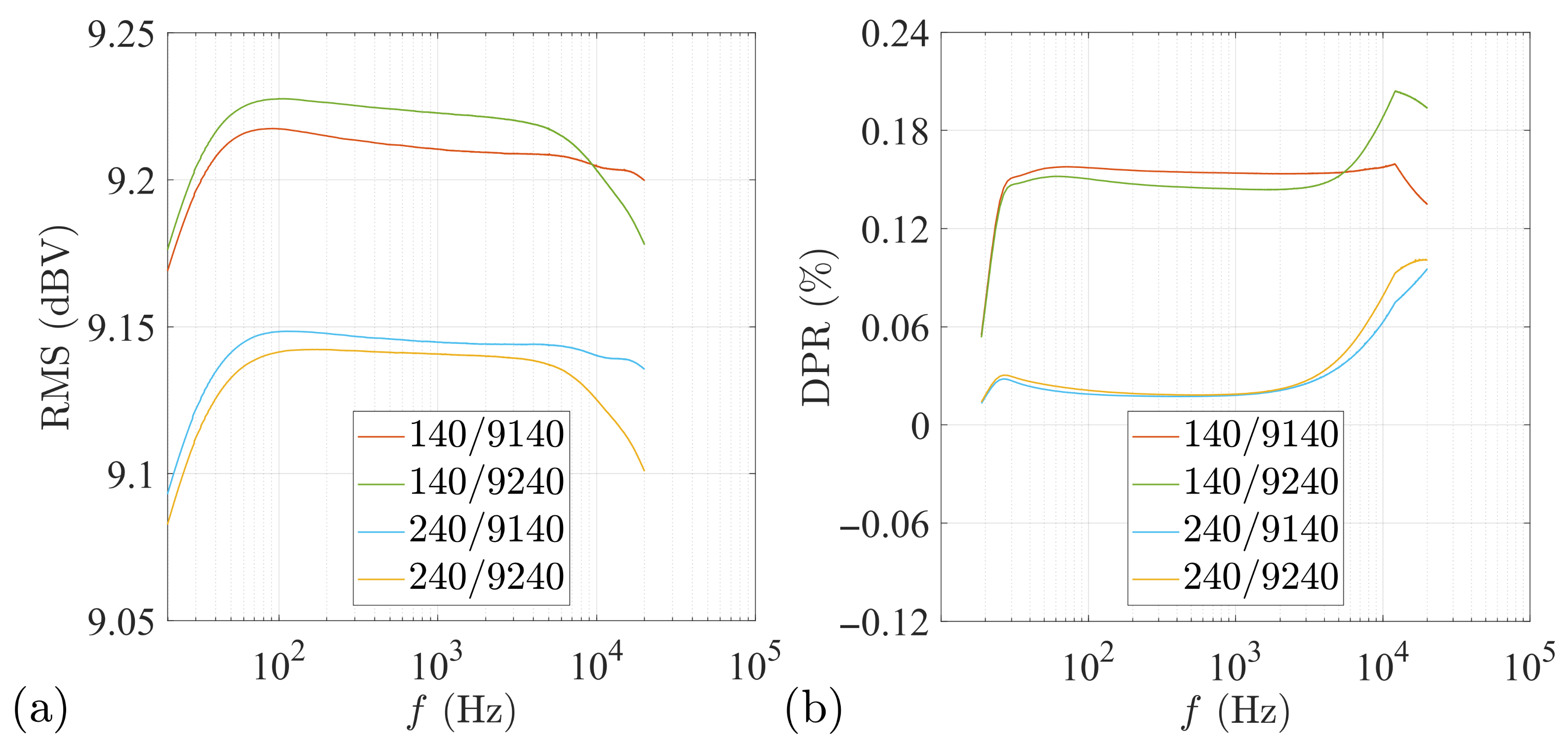
Figure 9 shows the amplitude–phase characteristics of the amplifier for the four configurations of transistor pairs used—IRFP140/IRFP9140 and IRFP240/IRFP9240—for an actual circuit with the preamplifier stage omitted. The circuit shows minimal gain differences (approximately 0.15 dB) for individual pairs of power transistors (Figure 9a). This is due to their non-uniform internal resistances, which translates directly into differences in the resting currents of the MOSFETs (in the case of components from different manufacturers or production batches, the matched pairs may show statistically insignificant gain differences). The circuit inverts the phase of the input signal (Figure 9b) and exhibits favorable phase characteristics, while in the case in question, an influence of internal parasitic capacitances of BJT and MOSFET transistors was observed. This becomes apparent in the faster phase drops for the extreme upper frequencies of the frequency response. Figure 10 shows the following: the frequency response of the amplifier for an output power of 1 W at load resistance R0 (Figure 10a) and the distortion contributed by the amplifier for all harmonic frequencies (Figure 10b). The lowest values of the DPR coefficient (below 0.1% in the whole passband under study) were recorded for the pairs 240/9140 and 240/9240.
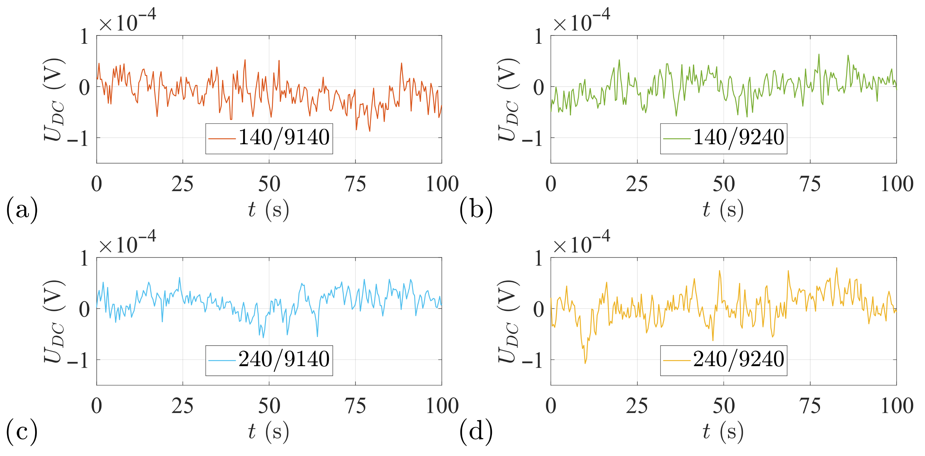
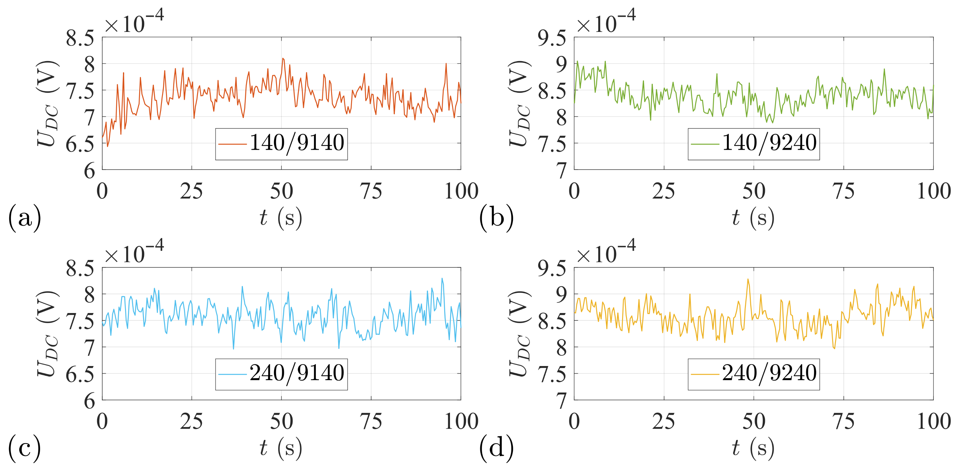
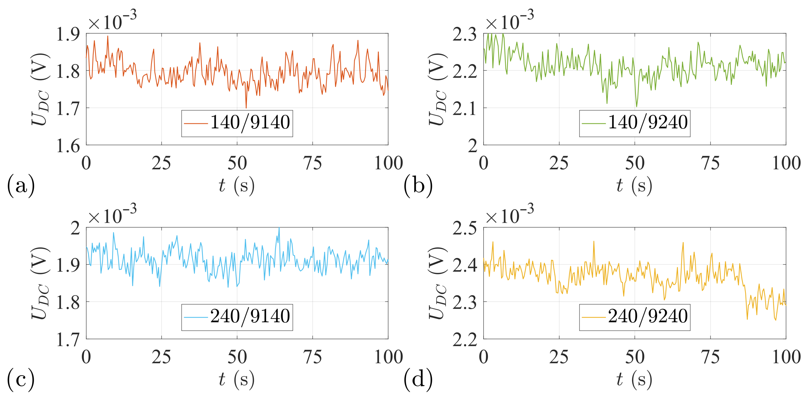
The measurements of voltage U D C on a load resistance of 8 Ω for the tested pairs of IRFP transistors are presented in Figure 11, Figure 12, Figure 13, Figure 14 and Figure 15. To allow these results to be correlated to other publications, we selected a typical value for load resistance R0, which is commonly used in analogue audio applications. It should be noted that for the intended application of the circuit, the value of R0 is different, but for obvious reasons, it will not be disclosed here. The tests were designed to verify (a) the ability of the amplifier to achieve the assumed values of the signal parameters (cf. Table 1) and (b) the amplifier’s self-balancing capability.
The measurement of U D C was first performed with input capacitors C7 and C8 shorted to ground, i.e., with no 1/2 D ˙ signal on the BJT transistors. Figure 11 presents sample 100 s waveforms of the voltage measured at R0—for each pair, its values are within ±100 μ V. The mean values of the voltages and their standard deviations for each transistor pair are shown in Table 3.
Figure 12, Figure 13 and Figure 14 show the measurements of U D C at R0 during active operation of the amplifier for an input signal frequency of 1 kHz—for the output power at an R0 of 1, 10, and 15 W, respectively. The mean values of the voltages and their standard deviations for these cases are shown in Table 4.
The higher values of U D C in comparison with those from the simulation studies can be explained, among other things, by the IRFP transistors not being paired in terms of electrical parameters but only being matched in physical complementary pairs. IRFP transistors are voltage-controlled transistors. The different gate opening voltages of IRFP transistors translate directly into differences in the pair’s resting currents. Consequently, the complementary pair is unable to develop the ideal symmetrical voltage to power itself. In the case in question, the two resistances controlled by the gate-opening voltage cyclically seek to deposit exactly half of the asymmetrical voltage on each other, which is only possible in an ideal scenario. Furthermore, the processing path is affected by interference and component noise, which further increases the value of U D C at R0. However, it should be noted that in none of the cases tested did the modulus of voltage U D C exceed 2.5 mV.
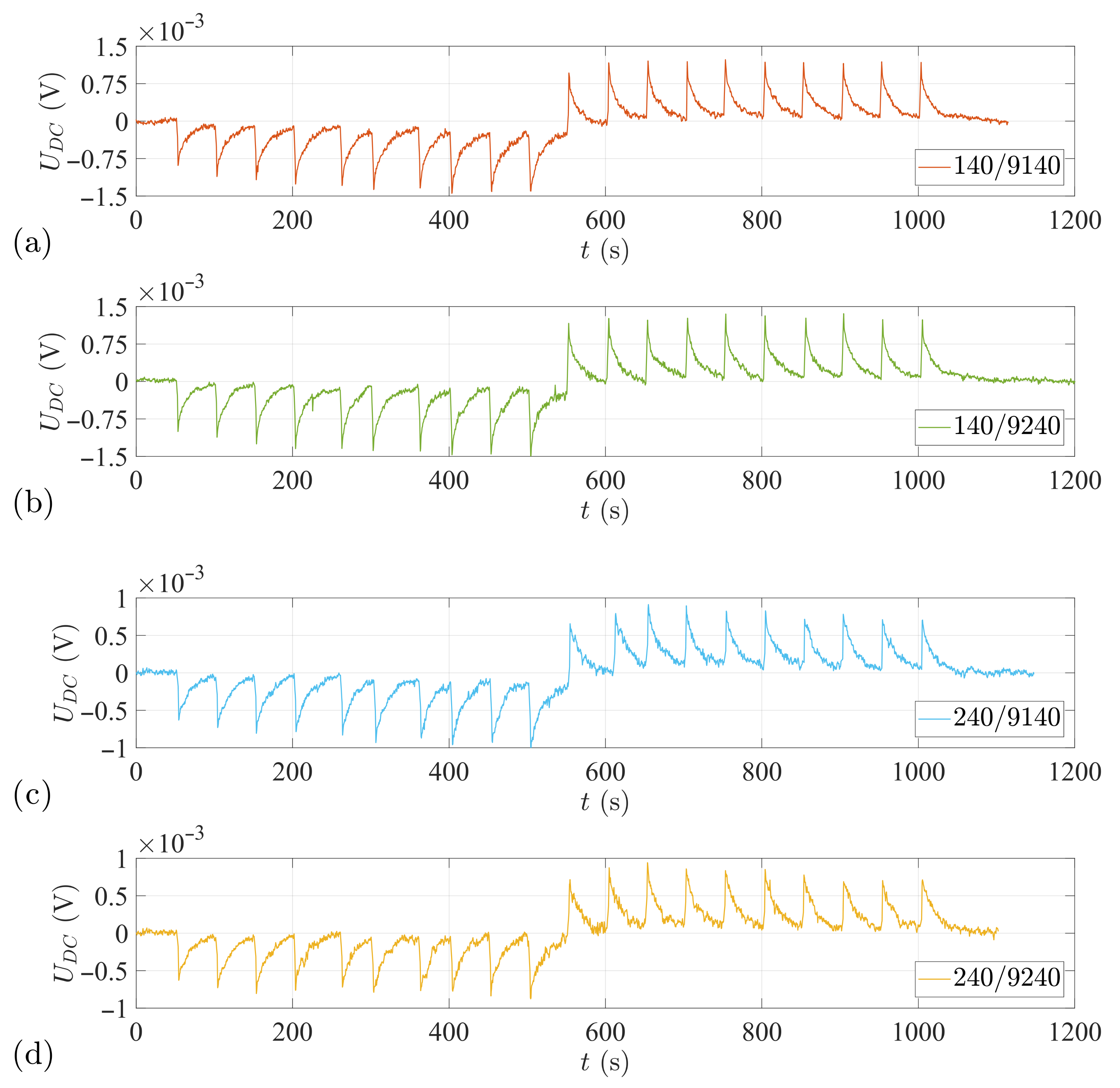
An important assumed property of the LF amplifier being tested is its self-balancing capability, which is defined as the ability to (a) bring the value of U D C at R0 to a minimum and to (b) maintain the minimum value of U D C during changes in the DC operating conditions of the system caused by changes in supply voltage. Sudden changes in supply voltage result in changes in the resting currents of the BJT and MOSFET transistors within the circuit. In turn, shifts in operating points lead to significant temperature gradients within the structures of nonlinear components.
The self-balancing capability of the low-frequency amplifier was verified according to the following procedure. A sinusoidal signal with a frequency of 1 kHz was applied to the input of the system under test loads with a resistance of 8 Ω . At time t = 0, the system was supplied with a nominal voltage of 70 V. The supply voltage was increased in increments of 1 V at 50 s intervals until 80 V was reached, which occurred around 550 s into the test. Then, also at 50 s intervals, the voltage was stepped down by 1 V until a nominal value of 70 V was reached, which occurred at 1000 s. The supply voltage spikes affected both the circuit with BJT transistors and the power follower with MOSFET transistors.
A diagram of the test is shown in Figure 15. The system shows a tendency toward a minimum value of U D C (and therefore, the desirable self-balancing capability) for all IRFP transistor pairs tested. In particular, regardless of the configuration, the system in question maintained U D C as low as possible despite sudden changes in the supply voltage. No undesirable increases in the value of U D C associated with temperature changes in the internal structures of the active elements were observed. Abrupt changes of the supply voltage were accompanied by momentary changes in the value of U D C at load resistances in the range of ±1.4 mV, which is easily noticeable on the waveforms over time presented in Figure 15. However, it should be emphasized that between the successive step changes for all the IRFP transistor pairs tested, in the range of supply voltage changes from 70 to 80 V (and consequently for resting current changes ranging from 0.33 to 1 A) and with an increase in operating temperature in the range of 38 to 65 C, the circuit spontaneously brought the value of U D C to within ±200 μ V. After the cessation of the step changes of supply voltage (at around 1100 s into the test), the value of U D C reached that recorded at the beginning of the test—for all pairs of IRFP transistors tested and at an operating temperature of approximately 38 C.

4. Conclusions

This paper presented a design of a new self-balancing AC component power amplifier with a minimum output DC component level (during operation both under and without load), which was intended for application in the launcher automation control circuit of a surface-to-air missile system. The amplifier has been designed using semiconductor technology based on a complementary MOSFET transistor pair. The system has been constructed and tested under laboratory conditions.
The device operates steadily and continuously throughout the entire range of the assumed signal processing band, with a sufficiently broad reserve of the frequency bandwidth. The topology of the system ensures very good phase characteristics of the amplifier over a broad band of processed LF signals and low DPRs at a high signal-to-noise ratio.
The proposed amplifier correctly maintains a minimum DC component output level regardless of (a) temporal and temperature-related load resistance changes; (b) changes in the load resistance character in terms of process LF signals; (c) changes to the LF control signal; and (d) idle current fluctuations resulting from supply voltage changes over time.
The system’s design does not include any additional modules interfering with the LF circuit of the amplifier, such as, e.g., external comparators correcting the output offset voltage level. Moreover, unlike typical design solutions, system fine-tuning takes place without the need to determine the minimum offset voltage level using an additional compensating potentiometer. DC operating conditions for nonlinear output elements are determined by setting the required DC biasing voltage value for the base of the transistors controlling the voltage stage.
The advantages of the proposed system include the following:
  • Eliminating tube technology, which is subject to relatively rapid aging;
  • Reduced power consumption owing to a significant reduction in supply voltage;
  • Eliminating power supply filter chokes and thus simplifying the power supply system;
  • Improved stability of electrical parameters by eliminating transformers that adapt the tube system to load or the next stage of the analog signal processing channel;
  • Reducing heat emission, thus limiting the impact of high temperatures on the operation of other electronic components and adjacent function blocks;
  • Significant simplification of system topology through improved operational indicators; and
  • Significant reduction of the geometric and mass parameters of the device relative to the original tube system.
In the longer term, the development of the proposed device into a dedicated integrated ASIC module is being considered. In civilian solutions, the application of such an amplifier would be possible, e.g., in robotic and automated systems in Manufacture 4.0, where due to higher system requirements and the use of increasingly complex communication protocols, stringent signal processing conditions are required [24,25].
It is worth noting that preliminary tests of the LF amplifier circuit presented herein coupled with other types of transistors indicated a possibility to further reduce the voltage of the output DC component while increasing the power in new versions of devices based on the application scheme. These considerations will be the subject of a subsequent publication.

Author Contributions

Conceptualization, P.Ż. and W.B.; methodology, W.B.; software, P.Ż.; validation, P.Ż. and W.B.; formal analysis, P.Ż.; investigation, P.Ż.; resources, P.Ż.; data curation, P.Ż.; writing—original draft preparation, P.Ż. and W.B.; writing—review and editing, W.B.; visualization, W.B.; supervision, W.B.; project administration, W.B.; funding acquisition, W.B. All authors have read and agreed to the published version of the manuscript.

Funding

This work was financed by Military University of Technology under research project UGB 22-894/2021.

Institutional Review Board Statement

Not applicable.

Informed Consent Statement

Not applicable.

Data Availability Statement

Not applicable.

Conflicts of Interest

The authors declare no conflict of interest.

Appendix A

Table A1. Component list of a proposed LF semiconductor amplifier.
No.LabelDescriptionParameters
1.R0loadn/a (8 Ω for test purposes)
2.R1metallized resistor10 Ω /3 W/5%
3.R2metallized resistor10 Ω /3 W/5%
4.R3metallized resistor100 k Ω /0.6 W/1%
5.R4metallized resistor100 k Ω /0.6 W/1%
6.R5metallized resistor100 Ω /0.6 W/1%
7.R6metallized resistor3.3 k Ω /0.6 W/1%
8.R7metallized resistor260 Ω /0.6 W/1%
9.R8metallized resistor100 k Ω /0.6 W/1%
10.R9metallized resistor510 k Ω /0.6 W/1%
11.R10metallized resistor5 k Ω /0.6 W/1%
12.R11metallized resistor5 k Ω /0.6 W/1%
13.R12metallized resistor1.5 k Ω /1 W/5%
14.R13metallized resistor1.5 k Ω /1 W/5%
15.R14metallized resistor100 k Ω /0.6 W/1%
16.R15metallized resistor100 k Ω /0.6 W/1%
17.R16metallized resistor270 Ω /1 W/5%
18.R17metallized resistor100 Ω /0.6 W/1%
19.R18metallized resistor100 Ω /0.6 W/1%
20.R19metallized resistor270 Ω /1 W/5%
21.R20ceramic resistor100 Ω /5 W/5%
22.R21ceramic resistor100 Ω /5 W/5%
23.R22metallized resistor330 Ω /1 W/5%
24.R23metallized resistor330 Ω /1 W/5%
25.R24ceramic resistor330 m Ω /5 W/5%
26.R25ceramic resistor330 m Ω /5 W/5%
27.R26ceramic resistor1 Ω /10 W/5%
28.R27ceramic resistor1 Ω /10 W/5%
29.POT1multi-turn assembly potentiometer10 k Ω /0.5 W/10%
30.POT2multi-turn assembly potentiometer5 k Ω /0.5 W/10%
31.C1electrolytic capacitor10,000 μ F/50 V
32.C2electrolytic capacitor10,000 μ F/50 V
33.C3electrolytic capacitor10,000 μ F/50 V
34.C4electrolytic capacitor10,000 μ F/50 V
35.C5polypropylene capacitor4.7 μ F/63 V/10%
36.C6ceramic capacitor33 pF/100 V/10%
37.C7polypropylene capacitor4.7 μ F/63 V/10%
38.C8polypropylene capacitor4.7 μ F/63 V/10%
39.C9electrolytic capacitor22,000 μ F/50 V
40.C10electrolytic capacitor22,000 μ F/50 V
41.C11electrolytic capacitor22,000 μ F/50 V
42.C12electrolytic capacitor22,000 μ F/50 V
43.OP1two-channel operational amplifierNE5532AP
44.T1bipolar NPN transistorBD139-16
45.T2bipolar PNP transistorBD140-16
46.T3P-MOSFET transistorIRFP9240 or IRFP9140
47.T4N-MOSFET transistorIRFP240 or IRFP140
Table A2. Component list of a LF tube amplifier.
No.LabelDescriptionParameters
1.R14OMLT resistor750 k Ω (750–820)/0.5 W/5%
2.R15OMLT resistor470 k Ω /0.5 W/5%
3.R16OMLT resistor1.3 k Ω /0.5 W/5%
4.R17OMLT resistor30 k Ω /0.5 W/5%
5.R18linear potentiometer470 k Ω /A/30%
6.R19OMLT resistor120 k Ω /0.5 W/5%
7.R20OMLT resistor120 k Ω /0.5 W/5%
8.R21OMLT resistor620 Ω /0.5 W/5%
9.R22OMLT resistor15 k Ω (12–20)/0.5 W/5%
10.R23OMLT resistor430 k Ω /0.5 W/5%
11.R24OMLT resistor220 k Ω /0.5 W/5%
12.R25OMLT resistor470 k Ω /0.5 W/5%
13.R26OMLT resistor200 Ω/2 W/5%
14.R32MMT thermal resistor3 k Ω /20%
15.C4MGBT capacitor47 nF/200 V/10%
16.C5MGBT capacitor47 nF/200 V/10%
17.C6MGBT capacitor47 nF/200 V/10%
18.C7MGBT capacitor47 nF/200 V/10%
19.C8MGBT capacitor2 μ F/160 V/10%
20.C13MGBT capacitor4 μ F/160 V/10%
21.C16KCOT capacitor360 pF (300–430)/250 V/5%
22.L2electron lamp6N2P-EW
23.L3electron lamp6N2P-EW
24.L4electron lamp6P1P-EW
25.L5electron lamp6P1P-EW
26.TR1transformern/a

References

  1. Pietrasieński, J.; Rodzik, D.; Bużantowicz, W. The Tactical and Technical Functioning Conditions of the S-200C Vega Missile System on the Modern Battlefield. Saf. Def. 2021, 7, 80–89. [Google Scholar] [CrossRef]
  2. Koruba, Z.; Szmidt, P. The Remote Control of the Artillery Rocket Set as a Strongly Nonlinear System Subject to Random Loads. Electronics 2021, 10, 1507. [Google Scholar] [CrossRef]
  3. Pang, C.; Shan, G.; Ma, W.; Xu, G. Sensor radiation interception risk control in target tracking. Def. Technol. 2019, 16, 695–704. [Google Scholar] [CrossRef]
  4. Bużantowicz, W. Tuning of a Linear-Quadratic Stabilization System for an Anti-Aircraft Missile. Aerospace 2021, 8, 48. [Google Scholar] [CrossRef]
  5. Turinskyi, O.; Skoryk, A. Design method of surface-to-air missiles using the object-oriented approach and electronic launch technology. Sci. Technol. Air Force Ukr. 2019, 2, 133–142. [Google Scholar] [CrossRef]
  6. Pomohaiev, I.; Tarshyn, V.; Skoryk, A. Improved method of semi-active homing of surface-to-air missiles with measuring target-missile range. Sci. Technol. Air Force Ukr. 2020, 4, 95–101. [Google Scholar] [CrossRef]
  7. Gapiński, D.; Koruba, Z. Control of Optoelectronic Scanning and Tracking Seeker by Means the LQR Modified Method with the Input Signal Estimated Using of the Extended Kalman Filter. Energies 2021, 14, 3109. [Google Scholar] [CrossRef]
  8. Sinclair, I. Electronics Simplified, 3rd ed.; Elsevier: Kidlington, Oxford, UK, 2011. [Google Scholar] [CrossRef]
  9. Karapenev, B.D. Studies of Low-Frequency Power Amplifier Class D with Operational Amplifiers and Transistors. J. Electr. Electron. Eng. 2017, 5, 170–179. [Google Scholar] [CrossRef] [Green Version]
  10. Baliga, B.J. Silicon RF Power MOSFETs, 1st ed.; World Scientific: Singapore, 2005. [Google Scholar] [CrossRef]
  11. Ramella, C.; Piacibello, A.; Quaglia, R.; Camarchia, V.; Pirola, M. High Efficiency Power Amplifiers for Modern Mobile Communications: The Load-Modulation Approach. Electronics 2017, 6, 96. [Google Scholar] [CrossRef] [Green Version]
  12. Camarchia, V.; Quaglia, R.; Piacibello, A.; Nguyen, D.P.; Wang, H.; Pham, A.V. A Review of Technologies and Design Techniques of Millimeter-Wave Power Amplifiers. IEEE Trans. Microw. Theory Tech. 2020, 68, 2957–2983. [Google Scholar] [CrossRef]
  13. De Forest, L. The Audion: A New Receiver for Wireless Telegraphy. Trans. Am. Inst. Electr. Eng. 1906, 25, 735–763. [Google Scholar] [CrossRef]
  14. Kahng, D. Electric Field Controlled Semiconductor Device. US Patent No. 3,102,230, 27 August 1963. [Google Scholar]
  15. Atala, M.M. Semiconductor Devices Having Dielectric Coatings. US Patent No. 3,206,670, 14 September 1965. [Google Scholar]
  16. Ye, P.D.; Yang, B.; Ng, K.K.; Bude, J.; Wilk, G.D.; Halder, S.; Hwang, J.C.M. GaN MOS-HEMT using atomic layer deposition Al2O3 as gate dielectric and surface passivation. Int. J. High Speed Electron. Syst. 2004, 14, 791–796. [Google Scholar] [CrossRef]
  17. Mimura, T. Development of High Electron Mobility Transistor. Jpn. J. Appl. Phys. 2005, 44, 8263–8268. [Google Scholar] [CrossRef]
  18. Lee, S.H.; Lim, J.W.; Kang, D.M.; Baek, Y.S. Technical Trends in Next-Generation GaN RF Power Devices and Integrated Circuits. Electron. Telecommun. Trends 2019, 34, 71–80. [Google Scholar] [CrossRef]
  19. Pearton, S.J.; Ren, F.; Tadjer, M.; Kim, J. Perspective: Ga2O3 for ultra-high power rectifiers and MOSFETS. J. Appl. Phys. 2018, 124, 220901. [Google Scholar] [CrossRef] [Green Version]
  20. Fujiwara, S.; Yamamoto, K.; Miyashita, M.; Yamabe, S.; Kabayashi, D. Power Amplifier. US Patent No. US 9,041,473 B2, 26 May 2015. [Google Scholar]
  21. Grebennikov, A. RF and Microwave Power Amplifier Design, 2nd ed.; McGraw Hill: New York, NY, USA, 2015. [Google Scholar]
  22. Lewis, G.K.; Olbricht, W.L. Development of a portable therapeutic and high intensity ultrasound system for military, medical, and research use. Rev. Sci. Instrum. 2008, 79, 114302. [Google Scholar] [CrossRef] [PubMed]
  23. Golub, G.H.; Van Loan, C.F. Matrix Computations, 3rd ed.; Johns Hopkins: Baltimore, MD, USA, 1996. [Google Scholar]
  24. Mulya, M.A.J.; Alam, B.R. Design of Low Noise Amplifier of a Broadband RF IC Transponder for RF Link in Manufacture 4.0. In Proceedings of the 2019 International Symposium on Electronics and Smart Devices (ISESD), Bali, Indonesia, 8–9 October 2019; pp. 1–4. [Google Scholar] [CrossRef]
  25. Borys, S.; Kaczmarek, W.; Laskowski, D. Selection and Optimization of the Parameters of the Robotized Packaging Process of One Type of Product. Sensors 2020, 20, 5378. [Google Scholar] [CrossRef] [PubMed]
Figure 1. Diagram of the LF tube amplifier.
Applsci 12 03532 g001
Figure 2. Side view of an anti-aircraft missile launcher.
Applsci 12 03532 g002
Figure 3. (a) Block scheme and (b) diagram of the designed LF semiconductor amplifier.
Applsci 12 03532 g003
Figure 4. Sample views of the LF power amplifier module.
Applsci 12 03532 g004
Figure 5. PCB layout design: (a) board with a preliminary amplifier system; and (b) LF amplifier motherboard.
Applsci 12 03532 g005
Figure 6. Numerically simulated: (a) amplitude; and (b) phase characteristic of the LF amplifier (including the pre-processing stage).
Applsci 12 03532 g006
Figure 7. Numerically simulated: (a) amplitude; and (b) phase characteristic of the LF amplifier (without the pre-processing stage).
Applsci 12 03532 g007
Figure 8. Voltage U D C determined by simulation at load R0 with input capacitors C7 and C8 shorted to ground for: (a) 140/9140; (b) 140/9240; (c) 240/9140; and (d) 240/9240 transistor pair.
Applsci 12 03532 g008
Figure 9. Measured: (a) amplitude and (b) phase characteristic of the LF amplifier.
Applsci 12 03532 g009
Figure 10. Measured: (a) RMS and (b) DPR of the LF amplifier.
Applsci 12 03532 g010
Figure 11. Voltage U D C measured at load R0 with input capacitors C7 and C8 shorted to ground for: (a) 140/9140; (b) 140/9240; (c) 240/9140; and (d) 240/9240 transistor pairs.
Applsci 12 03532 g011
Figure 12. Voltage U D C measured for 1 W of output power at load R0: (a) 140/9140; (b) 140/9240; (c) 240/9140; and (d) 240/9240 transistor pair.
Applsci 12 03532 g012
Figure 13. Voltage U D C measured for 10 W of output power at load R0: (a) 140/9140; (b) 140/9240; (c) 240/9140; and (d) 240/9240 transistor pair.
Applsci 12 03532 g013
Figure 14. Voltage U D C measured for 15 W of output power at load R0: (a) 140/9140; (b) 140/9240; (c) 240/9140; and (d) 240/9240 transistor pair.
Applsci 12 03532 g014
Figure 15. System response to supply voltage spikes for: (a) 140/9140; (b) 140/9240; (c) 240/9140; and (d) 240/9240 transistor pair.
Applsci 12 03532 g015
Table 1. Assumed parameter values for the LF amplifier under design.
ParameterValue
amplifier bandwidthfrom 20 Hz to 20 kHz
output signal power≥10 W
distortion product ratio<1%
DC level of output signal<2.5 mV
height × length × width (incl. mounting platform)120 × 210 × 300 mm
mass of the amplifier module (incl. frames and covers)<5 kg
Table 2. Numerical data for Figure 8.
Parameter of U DC 140/9140140/9240240/9140240/9240
mean value (V) 1.50 × 10 11 3.06 × 10 12 1.62 × 10 11 7.80 × 10 12
standard deviation (V) 9.74 × 10 12 6.55 × 10 12 6.98 × 10 12 6.57 × 10 12
Table 3. Numerical data for Figure 11.
Parameter of U D C 140/9140140/9240240/9140240/9240
mean value (V) 9.04 × 10 6 6.15 × 10 8 9.04 × 10 6 8.68 × 10 6
standard deviation (V) 2.64 × 10 5 2.33 × 10 5 2.26 × 10 5 3.21 × 10 5
Table 4. Numerical data for Figure 12, Figure 13 and Figure 14.
Working ConditionsParameter of U DC 140/9140140/9240240/9140240/9240
1.6 V/1 kHz/1 Wmean value (V) 2.14 × 10 4 1.92 × 10 4 2.05 × 10 4 2.66 × 10 4
standard deviation (V) 2.26 × 10 5 2.59 × 10 5 2.67 × 10 5 2.47 × 10 5
5.0 V/1 kHz/10 Wmean value (V) 7.33 × 10 4 8.60 × 10 4 7.55 × 10 4 8.62 × 10 4
standard deviation (V) 2.76 × 10 5 5.78 × 10 5 2.61 × 10 5 2.61 × 10 5
6.3 V/1 kHz/15 Wmean value (V) 1.79 × 10 3 2.23 × 10 3 1.91 × 10 3 2.36 × 10 3
standard deviation (V) 3.21 × 10 5 5.07 × 10 5 2.97 × 10 5 3.63 × 10 5
Publisher’s Note: MDPI stays neutral with regard to jurisdictional claims in published maps and institutional affiliations.