

Plasma Surface Modification of PDMS-Glass Microfluidic Chips for Oil Recovery Studies

 , ,
, ,
Abstract
:1. Introduction
2. Materials and Methods
2.1. Materials
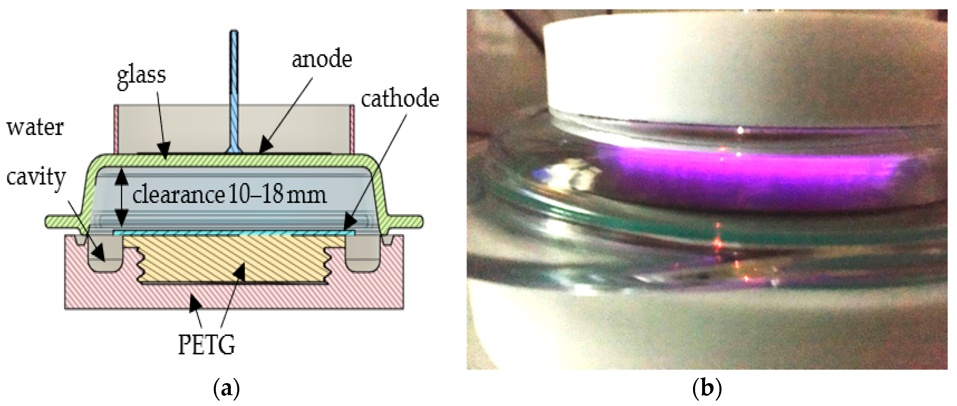
2.2. Plasma Laboratory Instrument and Chip Plasmaization
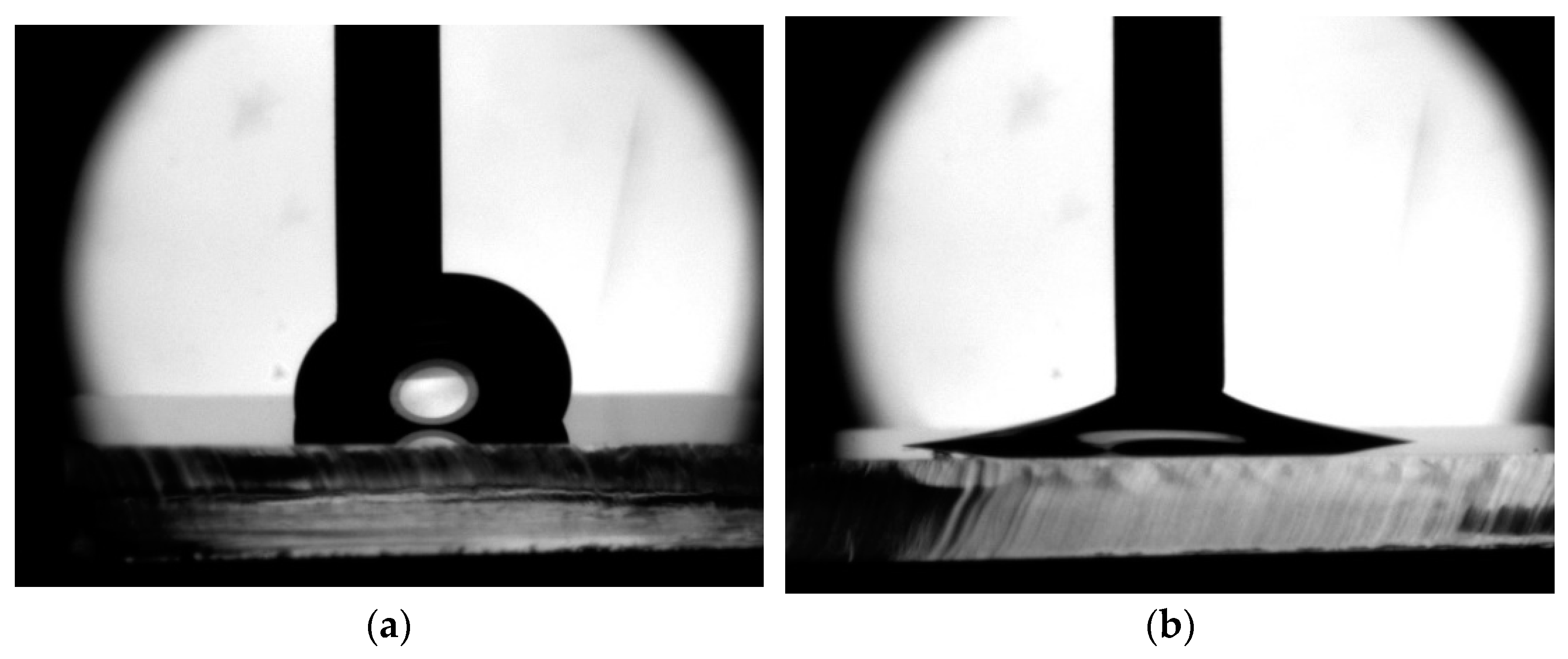
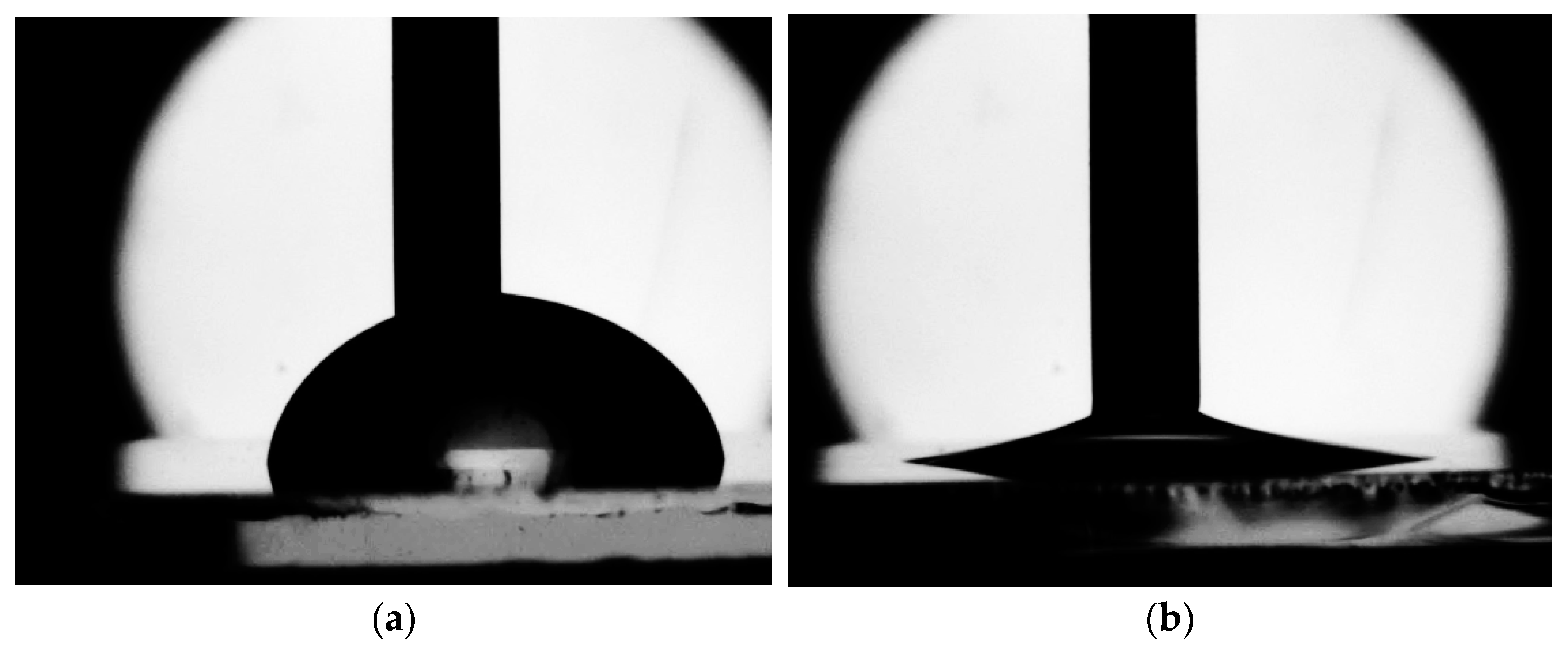
2.3. Measuring the Contact Angle of Advancing and Receiding
2.4. Problems and Solutions
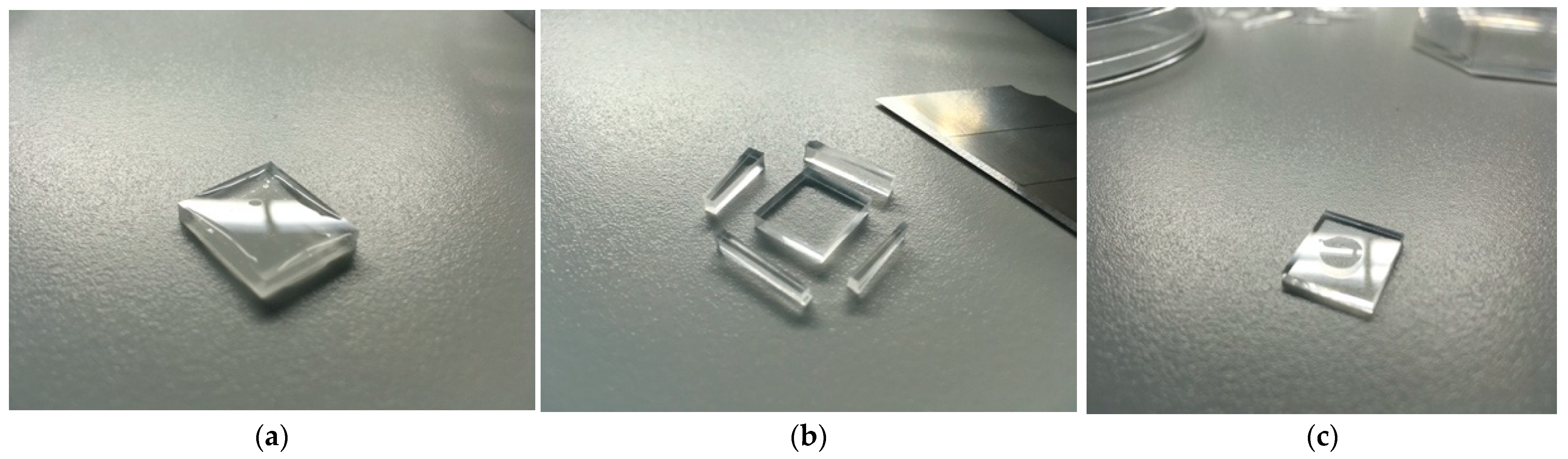
2.5. Topology and Chip Fabrication
2.6. Chip Surface Modification
2.7. Oil Displacement
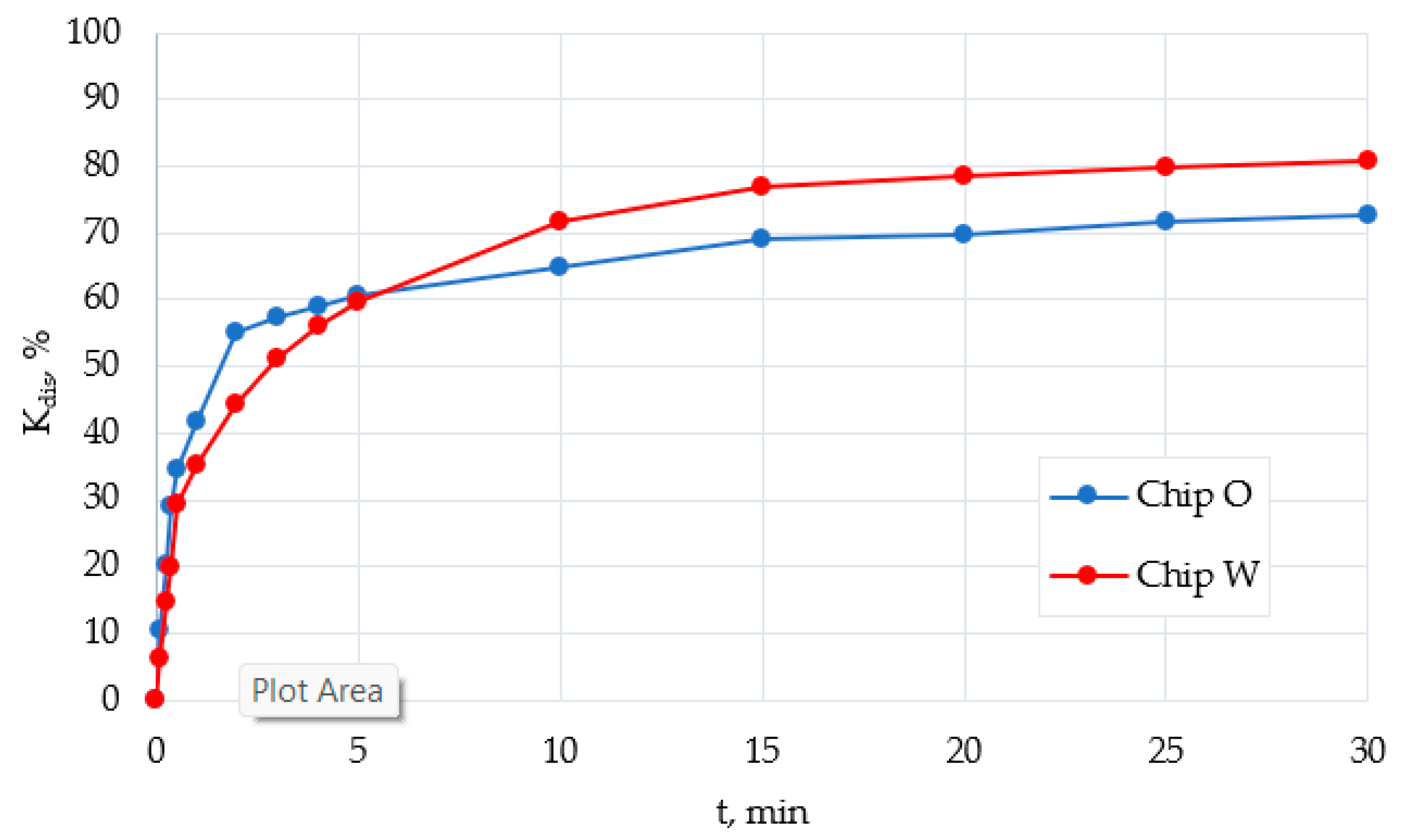
2.8. Photometric Estimation of Oil Displacement Efficiency (Kdis)
3. Results and Discussions
3.1. Surface Modification
3.1.1. PDMS
3.1.2. Glass
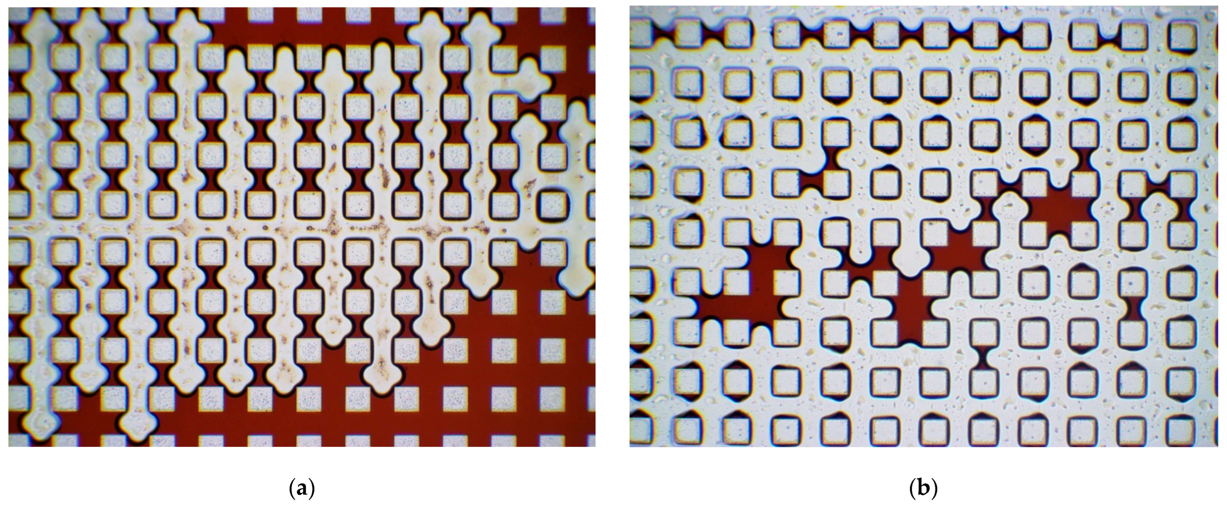
3.2. Modification of Chip Capillaries
4. Conclusions
- It is shown that with the help of plasma treatment it is possible to change the wetting angles of the walls of microfluidic chips in a very wide range, thereby simulating the conditions of both hydrophobic and hydrophilic rocks;
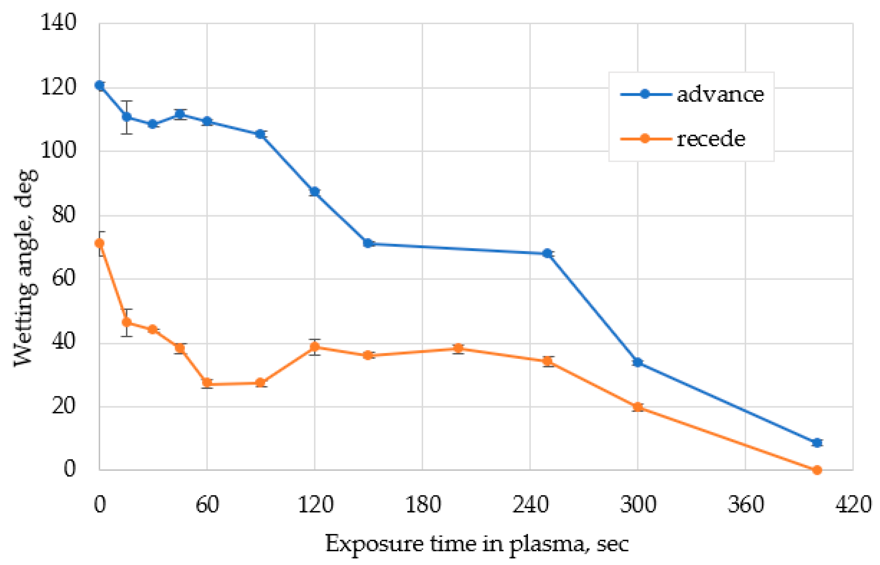
- PDMS has a very wide contact angle range from hydrophobic to super-hydrophilic: the contact angle decreases from 120° to 10°; receding angle—from 70° to 0° during plasma treatment;
- Glass in its original state is a hydrophilic material. It is shown that even short-term plasma treatment makes it possible to achieve superhydrophilicity of the glass surface. For 1 min of treatment, the contact angle decreases by more than 50º. This material is recommended for use at high pressures and relatively high temperatures due to its high strength, chemical resistance and the possibility of plasma-chemical surface modification;
- The study of the processes of oil displacement from hydrophilized chips showed that the patterns of water-oil flow in the treated and untreated chip differ significantly on the macro- and microscales. Despite the fact that the overall surface of the chips remains hydrophobic. It was shown that plasma treatment of a PDMS microfluidic chip leads to a significant change in the wetting characteristics of its surface. This in total leads to an increase in the oil displacement efficiency from the chip by about 10%.
Author Contributions
Funding
Institutional Review Board Statement
Informed Consent Statement
Data Availability Statement
Acknowledgments
Conflicts of Interest
References
- Choi, K.; Ng, A.H.; Fobel, R.; Wheeler, A.R. Digital microfluidics. Annu. Rev. Anal. Chem. 2012, 5, 413–440. [Google Scholar] [CrossRef] [PubMed]
- Barbulovic-Nad, I.; Yang, H.; Park, P.S.; Wheeler, A.R. Digital microfluidics for cell-based assays. Lab Chip 2008, 8, 519–526. [Google Scholar] [CrossRef]
- Uddin, M.J.; Bhuiyan, N.H.; Shim, J.S. Fully integrated rapid microfluidic device translated from conventional 96-well ELISA kit. Sci. Rep. 2021, 11, 1986. [Google Scholar] [CrossRef] [PubMed]
- Folch, A. Introduction to bioMEMS; CRC Press: Boca Raton, FL, USA, 2013. [Google Scholar]
- Ren, K.; Zhou, J.; Wu, H. Materials for microfluidic chip fabrication. Acc. Chem. Res. 2013, 46, 2396–2406. [Google Scholar] [CrossRef] [PubMed]
- Becker, H.; Locascio, L.E. Polymer microfluidic devices. Talanta 2002, 56, 267–287. [Google Scholar] [CrossRef] [PubMed]
- McDonald, J.C.; Whitesides, G.M. Poly (dimethylsiloxane) as a material for fabricating microfluidic devices. Acc. Chem. Res. 2002, 35, 491–499. [Google Scholar] [CrossRef] [PubMed]
- Xia, Y.; Whitesides, G.M. Soft lithography. Annu. Rev. Mater. Sci. 1998, 28, 153–184. [Google Scholar] [CrossRef]
- Cheng, J.Y.; Yen, M.H.; Wei, C.W.; Chuang, Y.C.; Young, T.H. Crack-free direct-writing on glass using a low-power UV laser in the manufacture of a microfluidic chip. J. Micromechanics Microengineering 2005, 15, 1147. [Google Scholar] [CrossRef]
- Guckenberger, D.J.; De Groot, T.E.; Wan, A.M.; Beebe, D.J.; Young, E.W. Micromilling: A method for ultra-rapid prototyping of plastic microfluidic devices. Lab Chip 2015, 15, 2364–2378. [Google Scholar] [CrossRef]
- Wang, T.; Chen, J.; Zhou, T.; Song, L. Fabricating microstructures on glass for microfluidic chips by glass molding process. Micromachines 2018, 9, 269. [Google Scholar] [CrossRef]
- Qin, D.; Xia, Y.; Whitesides, G.M. Soft lithography for micro-and nanoscale patterning. Nat. Protoc. 2010, 5, 491. [Google Scholar] [CrossRef] [PubMed]
- Ou, J.; Glawdel, T.; Ren, C.L.; Pawliszyn, J. Fabrication of a hybrid PDMS/SU-8/quartz microfluidic chip for enhancing UV absorption whole-channel imaging detection sensitivity and application for isoelectric focusing of proteins. Lab Chip 2009, 9, 1926–1932. [Google Scholar] [CrossRef] [PubMed]
- Arscott, S. SU-8 as a material for lab-on-a-chip-based mass spectrometry. Lab Chip 2014, 14, 3668–3689. [Google Scholar] [CrossRef] [PubMed]
- Pan, Y.J.; Yang, R.J. A glass microfluidic chip adhesive bonding method at room temperature. J. Micromechanics Microengineering 2006, 16, 2666. [Google Scholar] [CrossRef]
- Bamshad, A.; Nikfarjam, A.; Khaleghi, H. A new simple and fast thermally-solvent assisted method to bond PMMA–PMMA in micro-fluidics devices. J. Micromechanics Microengineering 2016, 26, 065017. [Google Scholar] [CrossRef]
- Abgrall, P.; Low, L.N.; Nguyen, N.T. Fabrication of planar nanofluidic channels in a thermoplastic by hot-embossing and thermal bonding. Lab Chip 2007, 7, 520–522. [Google Scholar] [CrossRef] [PubMed]
- Jia, Z.J.; Fang, Q.; Fang, Z.L. Bonding of glass microfluidic chips at room temperatures. Anal. Chem. 2004, 76, 5597–5602. [Google Scholar] [CrossRef]
- Allen, P.B.; Chiu, D.T. Calcium-assisted glass-to-glass bonding for fabrication of glass microfluidic devices. Anal. Chem. 2008, 80, 7153–7157. [Google Scholar] [CrossRef]
- Trinh, K.T.L.; Thai, D.A.; Chae, W.R.; Lee, N.Y. Rapid fabrication of poly (methyl methacrylate) devices for lab-on-a-chip applications using acetic acid and UV treatment. ACS Omega 2020, 5, 17396–17404. [Google Scholar] [CrossRef]
- Trinh, K.T.L.; Chae, W.R.; Lee, N.Y. Pressure-free assembling of poly (methyl methacrylate) microdevices via microwave-assisted solvent bonding and its biomedical applications. Biosensors 2021, 11, 526. [Google Scholar] [CrossRef]
- Bhattacharyya, A.; Klapperich, C.M. Mechanical and chemical analysis of plasma and ultraviolet–ozone surface treatments for thermal bonding of polymeric microfluidic devices. Lab Chip 2007, 7, 876–882. [Google Scholar] [CrossRef] [PubMed]
- Jiang, B.; Guo, H.; Chen, D.; Zhou, M. Microscale investigation on the wettability and bonding mechanism of oxygen plasma-treated PDMS microfluidic chip. Appl. Surf. Sci. 2022, 574, 151704. [Google Scholar] [CrossRef]
- Abdel–Fattah, E. Surface activation of poly (methyl methacrylate) with atmospheric pressure Ar+H2O plasma. Coatings 2019, 9, 228. [Google Scholar] [CrossRef]
- Abate, M.F.; Ahmed, M.G.; Li, X.; Yang, C.; Zhu, Z. Distance-based paper/PMMA integrated ELISA-chip for quantitative detection of immunoglobulin G. Lab Chip 2020, 20, 3625–3632. [Google Scholar] [CrossRef] [PubMed]
- Khayrullin, M.M.; Zakirov, T.R.; Grishin, P.A.; Shilov, E.D.; Bukatin, A.S. Methods for Studying Two-Phase Flows in Porous Media: Numerical Simulation and Experiments on Microfluidics Chips. In Proceedings of the SPE Russian Petroleum Technology Conference, Virtual, 26–29 October 2020. [Google Scholar]
- Xizhnyak, G.P.; Amirov, A.M.; Mosheva, A.M.; Melexin, S.V.; Chizhov, D.B. Influence of wettability on oil displacement efficiency. Bull. Perm Natl. Res. Polytech. Univ. Geol. Oil Gas Eng. Min. 2013, 12, 54–63. [Google Scholar] [CrossRef]
- Yakimov, A.S.; Pryazhnikov, A.I.; Pryazhnikov, M.I.; Minakov, A.V. Production of microfluidic chips from polydimethylsiloxane with a milled channeled surface for modeling oil recovery during porous rock waterflooding. J. Min. Inst. 2022, 253, 105–114. [Google Scholar] [CrossRef]
- Berdichevsky, Y.; Khandurina, J.; Guttman, A.; Lo, Y.H. UV/ozone modification of poly (dimethylsiloxane) microfluidic channels. Sens. Actuators B Chem. 2004, 97, 402–408. [Google Scholar] [CrossRef]
- Denisov, I.A.; Lukyanenko, K.A.; Yakimov, A.S.; Kukhtevich, I.V.; Esimbekova, E.N.; Belobrov, P.I. Disposable luciferase-based microfluidic chip for rapid assay of water pollution. Luminescence 2018, 33, 1054–1061. [Google Scholar] [CrossRef]
- Li, S.; Hu, J.; Liu, B. Use of chemically modified PMMA microspheres for enzyme immobilization. Biosystems 2004, 77, 25–32. [Google Scholar] [CrossRef]
- Velazco-Medel, M.A.; Camacho-Cruz, L.A.; Bucio, E. Modification of PDMS with acrylic acid and acrylic acid/ethylene glycol dimethacrylate by simultaneous polymerization assisted by gamma radiation. Radiat. Phys. Chem. 2020, 171, 108754. [Google Scholar] [CrossRef]
- Trantidou, T.; Elani, Y.; Parsons, E.; Ces, O. Hydrophilic surface modification of PDMS for droplet microfluidics using a simple, quick, and robust method via PVA deposition. Microsyst. Nanoeng. 2017, 3, 16091. [Google Scholar] [CrossRef] [PubMed]
- Jahangiri, F.; Hakala, T.; Jokinen, V. Long-term hydrophilization of polydimethylsiloxane (PDMS) for capillary filling microfluidic chips. Microfluid. Nanofluidics 2020, 24, 2. [Google Scholar] [CrossRef]
- Bodas, D.; Khan-Malek, C. Hydrophilization and hydrophobic recovery of PDMS by oxygen plasma and chemical treatment—An SEM investigation. Sens. Actuators B Chem. 2007, 123, 368–373. [Google Scholar] [CrossRef]
- Li, D.; Xiong, M.; Wang, S.; Chen, X.; Wang, S.; Zeng, Q. Effects of low-temperature plasma treatment on wettability of glass surface: Molecular dynamic simulation and experimental study. Appl. Surf. Sci. 2020, 503, 144257. [Google Scholar] [CrossRef]


| Time, min | Chip Primary Extracted in oil (O) * | Chip Primary Extracted in Water after Plasma Treatment (W) * |
|---|---|---|
| 1 |  |  |
| 5 |  |  |
| 10 | 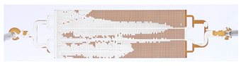 |  |
| 20 | 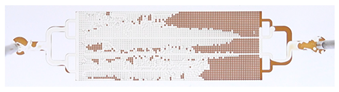 | 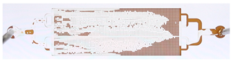 |
| 30 |  | 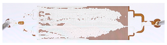 |
Disclaimer/Publisher’s Note: The statements, opinions and data contained in all publications are solely those of the individual author(s) and contributor(s) and not of MDPI and/or the editor(s). MDPI and/or the editor(s) disclaim responsibility for any injury to people or property resulting from any ideas, methods, instructions or products referred to in the content. |
© 2023 by the authors. Licensee MDPI, Basel, Switzerland. This article is an open access article distributed under the terms and conditions of the Creative Commons Attribution (CC BY) license (https://creativecommons.org/licenses/by/4.0/).
Share and Cite
Yakimov, A.S.; Pryazhnikov, A.I.; Pryazhnikov, M.I.; Skorobogatova, A.D.; Minakov, A.V. Plasma Surface Modification of PDMS-Glass Microfluidic Chips for Oil Recovery Studies. Appl. Sci. 2023, 13, 6365. https://doi.org/10.3390/app13116365
Yakimov AS, Pryazhnikov AI, Pryazhnikov MI, Skorobogatova AD, Minakov AV. Plasma Surface Modification of PDMS-Glass Microfluidic Chips for Oil Recovery Studies. Applied Sciences. 2023; 13(11):6365. https://doi.org/10.3390/app13116365
Chicago/Turabian StyleYakimov, Anton S., Andrey I. Pryazhnikov, Maxim I. Pryazhnikov, Angelica D. Skorobogatova, and Andrey V. Minakov. 2023. "Plasma Surface Modification of PDMS-Glass Microfluidic Chips for Oil Recovery Studies" Applied Sciences 13, no. 11: 6365. https://doi.org/10.3390/app13116365