Article

Current-Sensing Topology with Multi Resistors in Parallel and Its Protection Circuit

1
School of Automation Engineering, University of Electronic Science and Technology of China, Chengdu 611731, China
2
Forty-Fourth Research Institute, China Electronics Technology Group Corporation, Chongqing 401332, China
*
Authors to whom correspondence should be addressed.
Appl. Sci. 2023, 13(14), 8382; https://doi.org/10.3390/app13148382
Submission received: 16 June 2023 / Revised: 13 July 2023 / Accepted: 17 July 2023 / Published: 20 July 2023
(This article belongs to the Special Issue Progress in Electrical Energy Storage System)

Abstract

:
Current-sensing topology with multi resistors in series has limitations in improving the dynamic range of current acquisition, so a sensing topology with multi resistors in parallel is proposed. The overcurrent state of a parallel shunt circuit cannot be latched, resulting in protection hiccups. A dual threshold-detection circuit is designed to achieve protection state latching and self-recovery. The rectified mean circuit is applied for overcurrent magnitude detection and its validity is proved. But the delay and ripple of the output waveform of the rectified mean circuit may also cause protection hiccups. Combining Fourier series representation, Fourier transform and inverse transform, the time domain expressions of the output of the rectified mean circuit for three common waveforms are obtained. Furthermore, the estimation formulas for the residual ripple amplitude of the three waveforms are derived. In an experiment, the protection hiccup issue in parallel sensing topology was eliminated, while the time constants and hysteresis ratios of the protection circuits were properly set according to theoretical calculation results. With five parallel sensing resistors, the ratio of the maximum to minimum range of the single current channel reaches 1.28 × 10 4 , which is higher than counterparts with multiple series sensing resistors. The advantages of parallel sensing topology in improving dynamic range are confirmed.

1. Introduction

Measurement of the electric current is a key element in electrical systems. Current measurement can be achieved with various principles, including contacting type, sensing resistor and non-contacting type, Rogowski coil [1], Hall effect [2] and magnetoresistivity [3]. Due to the isolated design of the power analyzer at the digital signal transmission, the current-sensing stage does not need to be galvanic isolated. The advantages of non-contacting sensors cannot be utilized. The carefully designed sensing resistor has advantages such as high accuracy [4], good electromagnetic immunity [5] and high bandwidth [6,7]. Therefore, it is widely used in the current direct input channel of power analyzers. The sensing resistor and its overcurrent protection circuit are the focus of this study.
The power analyzer is commonly utilized for testing electrical equipment’s power performance, encompassing various aspects such as standby power consumption, startup inrush behavior, operational efficiency, power factor, harmonic interference and load regulation [8,9,10,11]. The standby power consumption of household appliances ranges from 0.2 W to 10 W [12,13], while their rated power consumption can vary from a few watts to several kilowatts. In cases of CNC machine tools, the power consumption during initial startup is usually several hundred watts, with inrush power peaking at 5.5 kW [14]. Considering a 220 V single-phase power supply, when measuring the aforementioned power parameters, the recorded currents fall within the range of hundreds of microamps to tens of amps.
In order to meet the large dynamic range requirement in current measurement, multiple sensing resistors were used in current channel design [15,16] or multiple current modules were designed [17,18] to achieve multiple ranges. As far as we know, the multiple sensing resistors in existing studies in the literature were connected in series [15,16,19,20]. The current flows through each resistor or its bypass circuit, so one of them must be capable of conducting the maximum allowed current in the maximum range. The increase in number of current sense resistors will lead to a tremendous increase in layout space and heat consumption. When the number of current sense resistors exceeds two, parallel connection would be a better choice. But the design of an overcurrent protection circuit is far more complicated than that of a series circuit.
The input stage of most electrical equipment items is an AC-DC rectifier [21]. If a power factor correction (PFC) circuit is not applied in the rectifier, the current shape will be significantly different from a sine wave, but with narrow pulses [22]. In cases of power supply testing, there are also various non-sinusoidal current waveforms existing, such as triangular, pulse and rectangular waves [23]. These waveforms have various crest factors. In order to meet the requirement of common waveform measurement, a high peak factor, such as 3, was selected for channel circuit design [16,17,18]. Magnitude detection is a necessary part of overcurrent protection circuit design. If peak detection is adopted, the actual protection threshold of waveforms with a low peak factor, such as square and DC wave, is three times the rated effective measurement range. This would damage current sense resistors due to overheating. An RMS-to-DC converter chip can measure the accurate effective value of the input waveform, but its cost is high and the working principle is complex. The dynamic response properties are not easy to be described via mathematical models and it is hard to estimate the response time and the residual ripple of the output waveform [24,25]. By contrast, the rectified mean circuit could be used to estimate the effective value roughly [24] and the circuit is pretty simple. It is more appropriate for magnitude detection in an overcurrent protection circuit.
In order to improve the dynamic range of current measurement, a current-sensing topology with multi resistors in parallel and the design method for its overcurrent protection circuit are proposed. No similar research has been found in the publicly available literature. In order to solve the hiccup issue in protection circuits of parallel sensing topology, a dual threshold-detection circuit is designed. Its working flow and the threshold calculation method are described in detail. For waveforms with various crest factors, the validities of the peak value and rectified mean value detection in the protection circuit are compared. A protection scheme combining these two magnitude-detection methods is proposed. The dynamic characteristics of the rectifier mean-detection circuit are simply determined by the first-order R-C low pass filter. To analyze the dynamic characteristics, Fourier series expressions are given for the absolute value of sinusoidal, triangular and periodic pulse waves. Then Fourier transform and inverse transform are used to obtain the time domain expressions of rectified mean output waveforms. With further transformation and calculation, the estimation formulas for output waveform ripples are obtained. They provide a basis for determining the hysteresis ratio of the comparison circuits. Finally, the advantages of the parallel sensing circuit in improving the dynamic range are verified in the experimental circuit. The conditions for eliminating protection hiccups are given.
Notation: R R denotes the ratio of maximum to minimum current range covered by a single resistor. I I N means the input current flowing through all sensing paths. I R j represents the current sensed by resistor R j and I T j represents the threshold of current sensed by R j while the involved protection circuit is triggered. I T j represents the threshold of the input current while the involved protection circuit is triggered. C F and W F denote the crest factor and waveform factor of waveforms, respectively. P F denotes the peak factor of the measurement circuit for a specified range. X P K , X R M S and X R M are the peak value, effective value and rectified mean value of waveforms, respectively. V R A and V R A represent the ripple amplitude evaluated by complete calculation and estimation formulas respectively, for output waveforms of the rectified mean circuit. K R A denotes the ratio of V R A to V R A . γ denotes the relative error of V R A to V R A . R R P means the ratio of V R A to X R M . δ H means the ratio of half the comparator hysteresis voltage to initial threshold voltage. For all above notations, the subscript j can be replaced by 1 or 2.

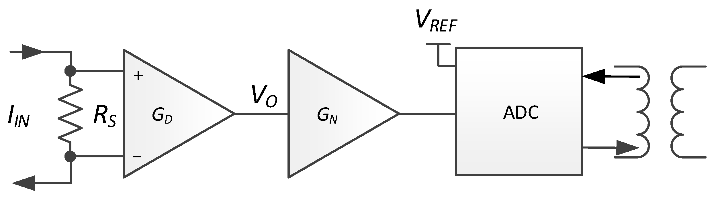
2. Materials and Methods

2.1. Parallel or Series Multi Resistor Current-Sensing Topology

In order to meet the requirements of accurate power measurement from no load to full load of various equipment items, the current channel of the power analyzer needs to be designed with multiple measuring ranges from a few milliamps to tens of amps. The typical circuit of the current channel is shown in Figure 1. A resistor R S is used to convert input current I I N into voltage. The voltage is amplified by the differential amplifier G D and the post-amplifier G N and then fed into ADC for digital quantization. After galvanic isolation, the digital output of ADC is sent to a digital process unit. Pins and solders usually have much higher temperature drift relative to the resistance body. In order to improve measurement accuracy, when the resistance of R S is low, a four-wire resistor should be used. That is why the first stage may be a differential amplification circuit.
To reduce load effect and temperature rise, the resistance of the current sense resistor is expected to be as low as possible. For an input current of tens of amps, the resistance is only a few milliohms. With a single current sense resistor (e.g., 2 m Ω ) and a milliampere level input current (e.g., 10 mA), it requires amplifying the sensed voltage (20 μ V) several hundred thousand times ( G N × G N = 10 5 ) to several volts (e.g., 2 V) to meet the ADC input range (as determined by the reference voltage V R E F ). This puts forward ultra-high requirements to parameters such as power supply noise, amplifier input noise and temperature drift, to guarantee the measurement accuracy. To solve this contradiction, the current channel of the power analyzer usually adopts multiple current sense resistors. Each resistor only covers a section of measurement ranges. Define the range ratio R R as:
R R = R M A X / R M I N
R M A X is the maximum range covered by one current sense resistor, while R M I N is the minimum range covered by the same resistor.
The lower value of R R induces lower requirements for the amplification circuit. In power analyzer design, R R = 2 ∼10 is usually taken.

2.1.1. Current-Sensing Topology with Multi Resistors in Series

Several current sense resistors were in series connection in the known power analyzer [15,16]. A current-sensing circuit with two resistors is shown in Figure 2, while the overcurrent protection circuit is included.
In Figure 2, R 2 has a higher resistance value, covering lower ranges, while R 1 has a lower value, covering higher ranges. C T R 2 is the switch control signal from the module controller. When the user selects lower ranges, C T R 2 is low level and switch S 2 is open. The input current flows through R 2 . Voltage V O 2 is selected and sent to the latter circuit. When switching to higher ranges, the switch S 2 is closed. Most current is bypassed through S 2 and voltage V O 1 is selected. Whether the switch S 2 is open or closed, all current flows through R 1 . Therefore V O 1 can be monitored via the magnitude-detection circuit and overcurrent protection can be performed by comparing the magnitude with threshold voltage V T 2 .
Let the maximum allowed sensing current of resistor R 2 be I T 2 . When the monitoring voltage V O 1 meets (2), P T 2 switches to a high level. The switch S 2 is forced to close to protect R 2 from overheating.
V O 1 > I T 2 × R 1
D 1 and D 2 are bi-direction freewheeling diodes. Let the forward voltage of diodes be V F . When the input current exceeds the threshold current I T 2 and the protection circuit has not yet activated, D 1 and D 2 limit the current I R 2 flowing through R 2 as follows:
I R 2 V F / R 2
Through the above protection circuit, when the input current is high and the user chooses a lower range, bypassing of the current is forced. This prevents the current sense resistor R 2 from being damaged by overheating.
The series sensing circuit in Figure 2 can be extended to have more sensing resistors R 3 , R 4 , …, more bypass switches K 3 , K 4 , … and more freewheeling diodes D 3 / D 4 , D 5 / D 6 , … No matter how many sensing resistors there are, R 1 can always detect the threshold current I T 3 , I T 4 , … The corresponding sensing resistors can be overcurrent protected by the combination of magnitude detection and comparison circuits similar to Figure 2.
For the series sensing method, the protection circuit is easy to design. But there are two drawbacks: Each high side sensing resistor needs a bypass switch and two freewheeling diodes. On the other hand, all these switches and diodes need to conduct the maximum input current (usually tens of amperes) continuously or transitorily, respectively, when the highest range is selected. That is, these switches and diodes would have considerable size and need heat dissipation design. As the number of sensing resistors increases, the layout space and power dissipation of these switches and diodes will be far beyond the sensing resistors.
Therefore, current sensing with multi resistors in series is generally only used in the case of 2∼3 sensing resistors [15,16]. For further expansion of the dynamic range of current measurement, this article proposes a current-sensing prototype with multi resistors in parallel. When the number of sensing resistors increases, the layout space and power consumption of switches and diodes can be significantly reduced compared with the series counterpart.

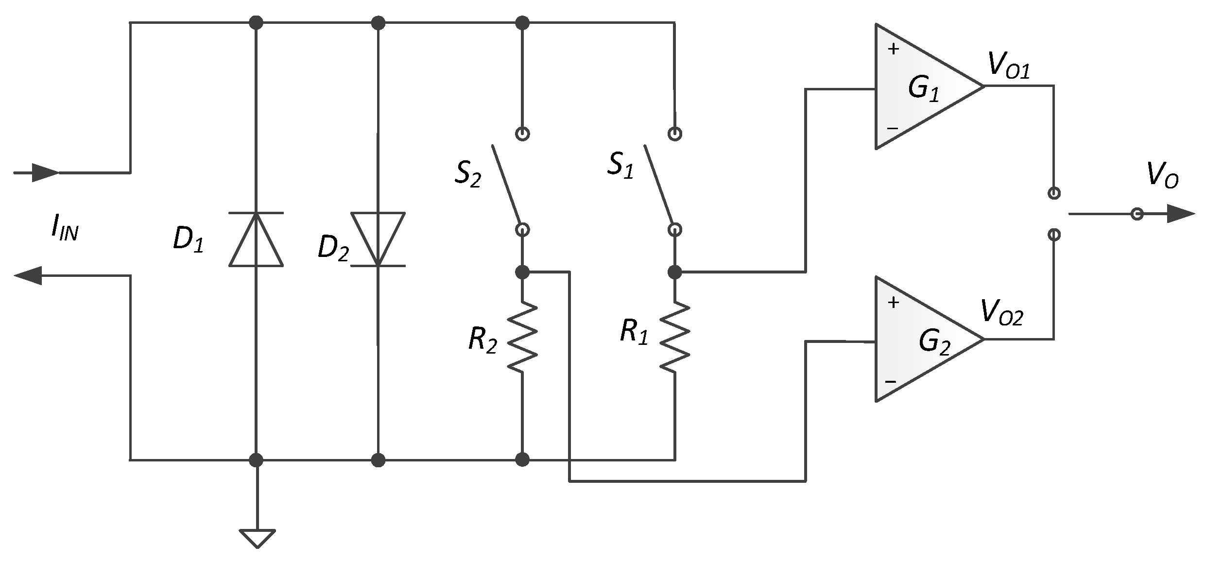
2.1.2. Current-Sensing Topology with Multi Resistors in Parallel

When multi sensing resistors are connected in parallel, the current flows only through the selected switch and sensing resistor. Figure 3 shows the case with two resistors.
In Figure 3, if the value of the sensing resistor is low, a four-wire resistor should still be used. The corresponding gain circuit G 1 or G 2 needs to be a differential amplification circuit. R 2 has higher resistance value, covering lower ranges, while R 1 has lower value, covering higher ranges. When a user selects lower ranges, the switch S 2 is closed and S 1 is open. The input current flows through S 2 and R 2 . Voltage V O 2 is selected. When switching to higher ranges, the switch S 1 is closed and S 2 is open. Voltage V O 1 is selected. D 1 and D 2 are bi-direction freewheeling diodes. They provide current paths for moments when both S 1 and S 2 are open.
In the parallel sensing circuit, the freewheeling diodes are shared by all sensing resistors, so there is a lower component count compared to the series counterpart. On the other hand, when there are more sensing resistors R 3 , R 4 , … and more switches K 3 , K 4 , …, each switch only needs to be capable of conducting a current within the corresponding ranges. Only S 1 is conducting when the highest range is selected. Compared with all switches conducting in a series circuit in this case, the parallel sensing circuit has significant advantages in terms of layout space and heat dissipation.
In Figure 3, the sensing resistor is connected in series with the switch. If the selected switch is switched off for overcurrent protection, the current would flow through diodes D 1 and D 2 . The forward voltage of diodes is considerably higher than the voltage drop of the original sensing path. For high input current, the power consumption of diodes would be too high to be dissipated. Therefore, the higher range’s sensing path should be switched on for overcurrent protection. This works as in following steps:
  • The initial condition: A lower range is selected and S 2 is closed. Let the maximum allowed current of sensing resistor R 2 be I T 2 . When the sensed current I R 2 > I T 2 , the switch S 1 is forced to close.
  • Then, the current is divided into both resistors R 1 and R 2 . The current values are calculated by Equations (4) and (5) respectively, where R S 1 and R S 2 are the conduction resistance of S 1 and S 2 . Since R S 1 + R 1 is generally 1/10∼1/4 times R S 2 + R 2 , most of the current is diverted to the sensing path of S 1 and R 1 to prevent the damage of S 2 and R 2 due to overheating.
I R 1 = I I N × ( R S 2 + R 2 ) / ( R S 2 + R 2 + R S 1 + R 1 )
I R 2 = I I N × ( R S 1 + R 1 ) / ( R S 2 + R 2 + R S 1 + R 1 )
When the above protection mechanism is adopted, the protection hiccup would occur as follows:
  • While S 1 is closed, the current sensed by R 2 is decreased to I R 2 = (1/11∼1/5) × I I N . In most cases, I R 2 is now lower than I T 2 . The overcurrent condition is not met any more. The switch S 1 returns to open.
  • After S 1 is open, I R 2 = I I N > I T 2 . The protection will be triggered again to make S 1 closed.
  • The above two steps occur alternately. This is called protection hiccup.
A protection hiccup appears because the overcurrent state could not be latched. To improve this, a protection circuit with dual threshold detection is designed, as shown in Figure 4.
In Figure 4, S 1 is closed at a high level of control input and vice versa. C T R 1 is the switch control signal from the module controller. V O 1 and V O 2 are sent to magnitude-detection circuits and then compared with voltage threshold V T 1 and V T 2 , respectively. These two overcurrent indication signals P T 1 and P T 2 are used to carry out an OR operation with C T R 1 and then to control S 1 . Switch S 1 is closed while any one of these three signals is high level. The working principle in detail is as follows:
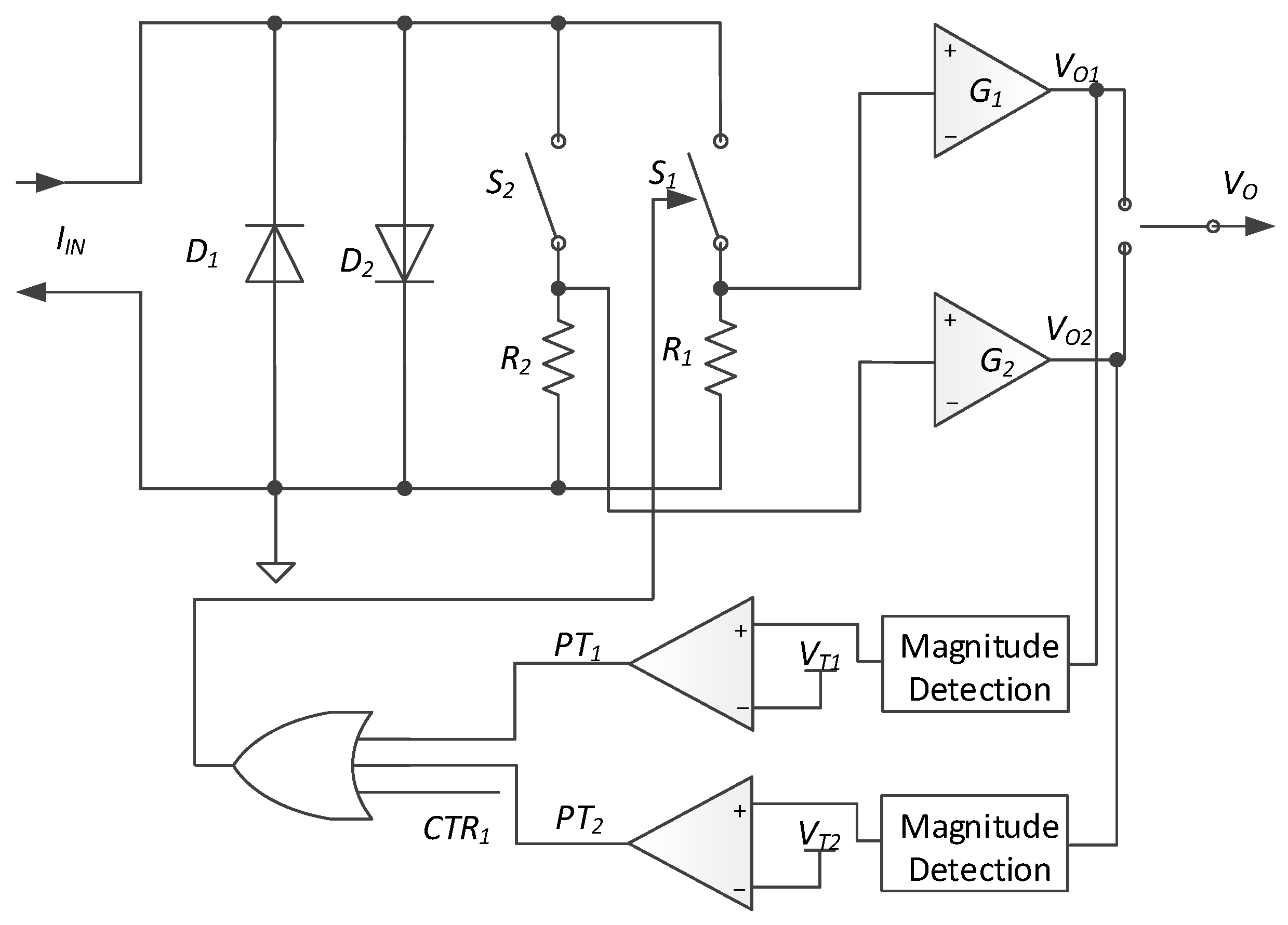
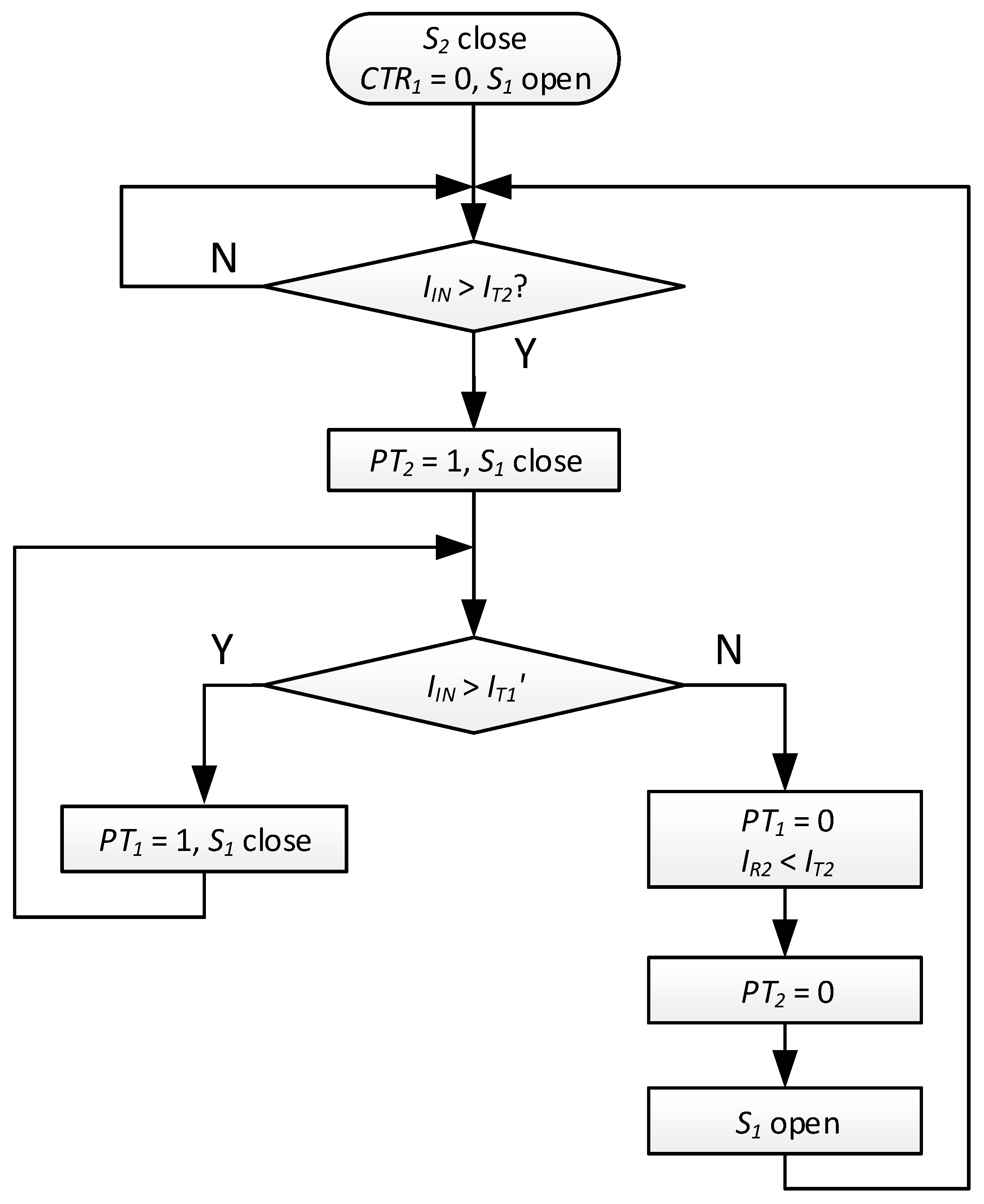
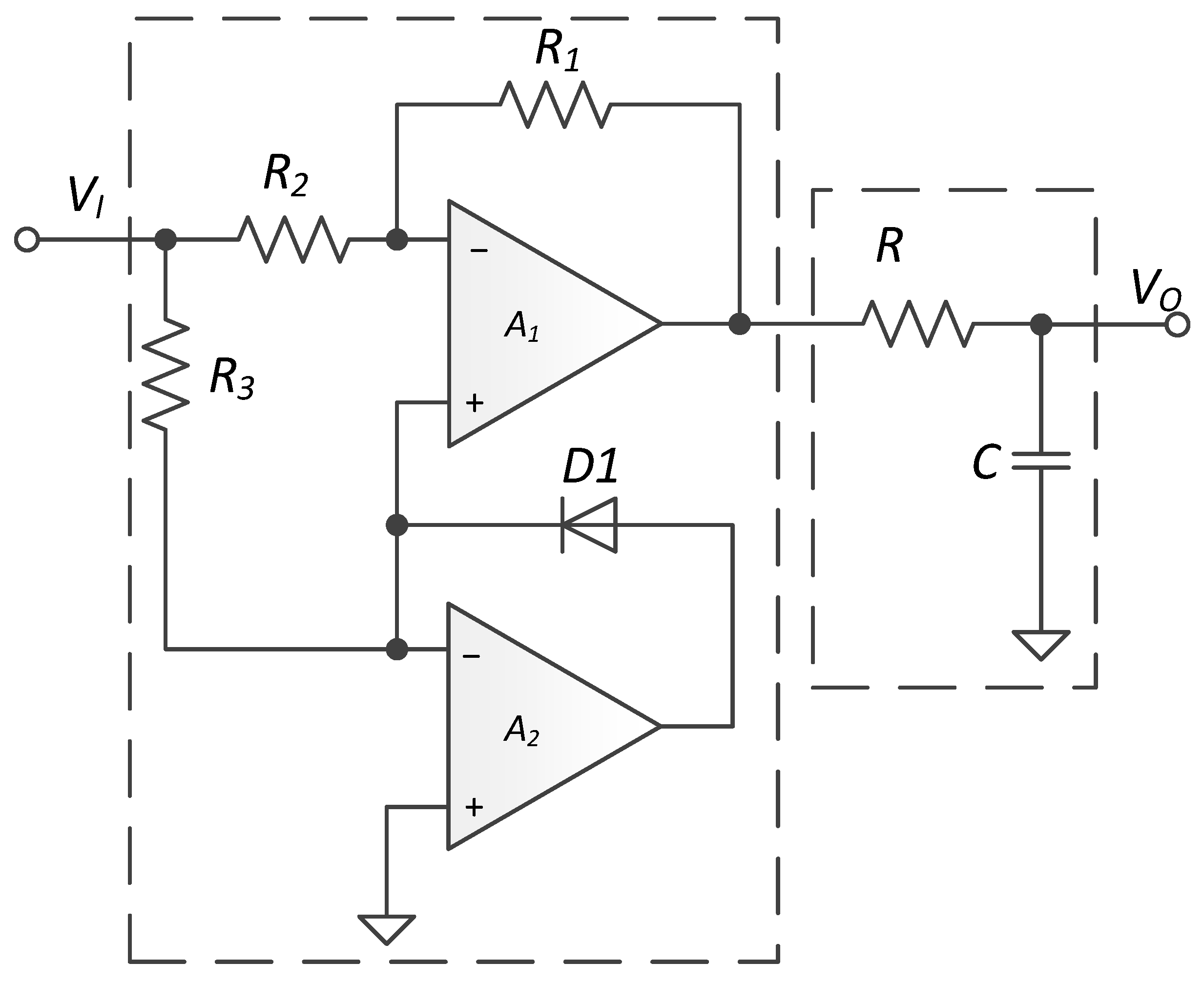
  • The initial condition: A lower current range is selected. C T R 1 is low level. S 2 is closed and S 1 is open.
  • When I R 2 = I I N > I T 2 , the overcurrent indication signal P T 2 changes from low to high level. The relation between I I N and I R 1 is given by:
    I I N = I R 1 × ( R S 2 + R 2 + R S 1 + R 1 ) / ( R S 2 + R 2 )
    When protection occurs, define the input threshold current I T 1 for P T 1 transformation as:
    I T 1 = I T 1 × ( R S 2 + R 2 + R S 1 + R 1 ) / ( R S 2 + R 2 )
  • Let I T 1 be slightly lower than I T 2 . Figure 5 shows the working flow of overcurrent protection.
As shown in Figure 5, the protection state is maintained while I I N > I T 2 and exits automatically whenever I I N < I T 1 . The protection hiccup mentioned before is eliminated. The amplifier gains G 1 and G 2 and compare thresholds V T 1 and V T 2 should be carefully designed to ensure I T 1 < I T 2 .
The work flow in Figure 5 is based on the condition that the delay of the magnitude-detection circuit and the residual ripple of the detection output are not considered. They may also cause protection hiccups. So the magnitude-detection circuit and its dynamic response to various waveforms are further studied in the next subsection. The complete condition for eliminating protection hiccups is shown in the results section.
To sum up, if the number of sensing resistors is higher than 2, the parallel sensing circuit requires a smaller layout space and lower heat dissipation than the series counterpart. But the protection circuit is much more complicated and needs to be carefully considered in design.

2.2. Rectified Mean Magnitude Detection

The crest factor C F is defined as the ratio of the waveform peak value X P K to the effective value X R M S :
C F = X P K / X R M S
Peak factor P F is defined as the ratio of measurement peak value to effective value for a specified range:
P F = I P K / I R M S
I P K is the maximum instantaneous current covered by this range, indicating the measurement span of I P K I P K . The waveform exceeding the span would be distorted. I R M S is the maximum heat equivalent current covered by this range. It depends on the heat dissipation property of the sensing resistors and conduction switches. If I R M S is significantly exceeded for a long time, the components in the sensing path may be damaged.
The rectified mean circuit could be adopted as the magnitude-detection circuit in Figure 2 and Figure 4. It is a rough method for effective value measurement, as shown in Figure 6.
The circuit in Figure 6 is divided into two stages, each located in a dotted box. The first stage is a precision rectifier circuit constructed with two operational amps, where R 1 and R 2 have equal resistance value. It is also called the absolute value circuit. The second stage is a first-order low-pass filter composed of a resistor R and a capacitor C and is called the average value circuit.

2.2.1. Protection Validity of Rectified Mean Detection

Both the input and output of the rectified mean-detection circuit are voltages. Let the input voltage V I be x ( t ) and the output voltage V O be y ( t ) .
Common waveforms under test include sine, triangular and periodic pulse waves. The expressions are (10)–(12), respectively:
x ( t ) = A sin ω 0 t
x ( t ) = 4 A ( t N T ) / T , N T t < N T + T / 4 2 A 4 A ( t N T ) / T , N T + T / 4 t < N T + 3 T / 4 4 A + 4 ( A t N T ) / T , N T + 3 T / 4 t < N T + T
x ( t ) = A , N T t < N T + D T / 2 A , N T + T / 2 t < N T + T / 2 + D T / 2 0 , o t h e r s
where N is an integer, T is the waveform period, ω 0 = 2 π / T , and D is the duty cycle of periodic pulse wave.
Take A = 1 , T = 0.1 s, D = 0.5 (the same values in Figures 8 and 9). The three waveforms are shown as Figure 7.
The effective and rectified mean values of waveforms can be calculated with Equations (13) and (14), respectively.
X R M S = 0 T x 2 ( t ) T
X R M = 0 T x ( t ) T
Form factor W F is defined as the ratio of effective value to rectified mean value of waveforms:
W F = X R M S / X R M
The three waveforms are calculated through Equations (13)–(15) and the results are shown in Table 1.
If the rectified mean circuit in Figure 6 is applied for rough measurement of the effective value and the form factor of the sine wave is used as the conversion coefficient from the rectified mean value to the effective value, the relative errors e R of other waveforms are as in Table 1.
e R = 1.111 X R M X R M S X R M S
If the rectified mean circuit is applied for measurement of the effective value and all waveforms with the same effective value are set as the input, the DC or periodic pulse waveform with D = 1 (that is the square wave) would result in the highest output. Therefore, To avoid protection lag, the protection thresholds in Figure 2 and Figure 4 should be calculated based on DC or square wave. The actual protection threshold of various waveforms with the same effective value V 0 is shown in Table 2:
In Table 2, e R M represents the relative error between the actual protection point and the threshold. It was calculated as follows:
e R M = V 0 X R M 1
The crest factor of the periodic pulse at D = 1 / 9 is just 3. e P K represents the relative error between the actual protection point and the threshold, when the peak-detection circuit is applied for magnitude detection and the protection threshold is set based on periodic pulse at D = 1 / 9 . It was calculated as follows:
e P K = 3 V 0 X P K 1
e R M and e P K can be used to indicate the protection validity of these two magnitude-detection methods. The higher the value, the worse the validity. As concluded from the data in Table 2, when the rectified mean circuit is used for magnitude detection, it has better protection validity for most waveforms, such as DC, sine, triangular and periodic pulse with D > 1 / 3 . For the periodic pulse with D < 1 / 3 , peak detection results in better protection validity. When D = 1 / 3 , these two magnitude-detection methods have the same validity and the actual protection point is 3 times the threshold.
Therefore, the overcurrent protection method combing rectified mean and peak detection should be used. Peak detection does not need to be performed through a hardware circuit as in Figure 2 and Figure 4. It can be executed by monitoring the real-time sample value of ADC. While the full scale sampling value is met, the protection can be executed by changing the signal level of C T R N (N is 1 or 2). It has similar timeliness to the hardware circuit because neither storage nor a computing module is required to process the sample value.
In summary, with the combination of rectified mean-detection circuit and peak detection via ADC sample value, overcurrent protection for common current waveforms can be realized. The thermal design of sensing resistors and switches shall ensure that they can conduct a current at 3 times the rated value continuously without damage, in response to periodic pulse at a specific duty cycle.

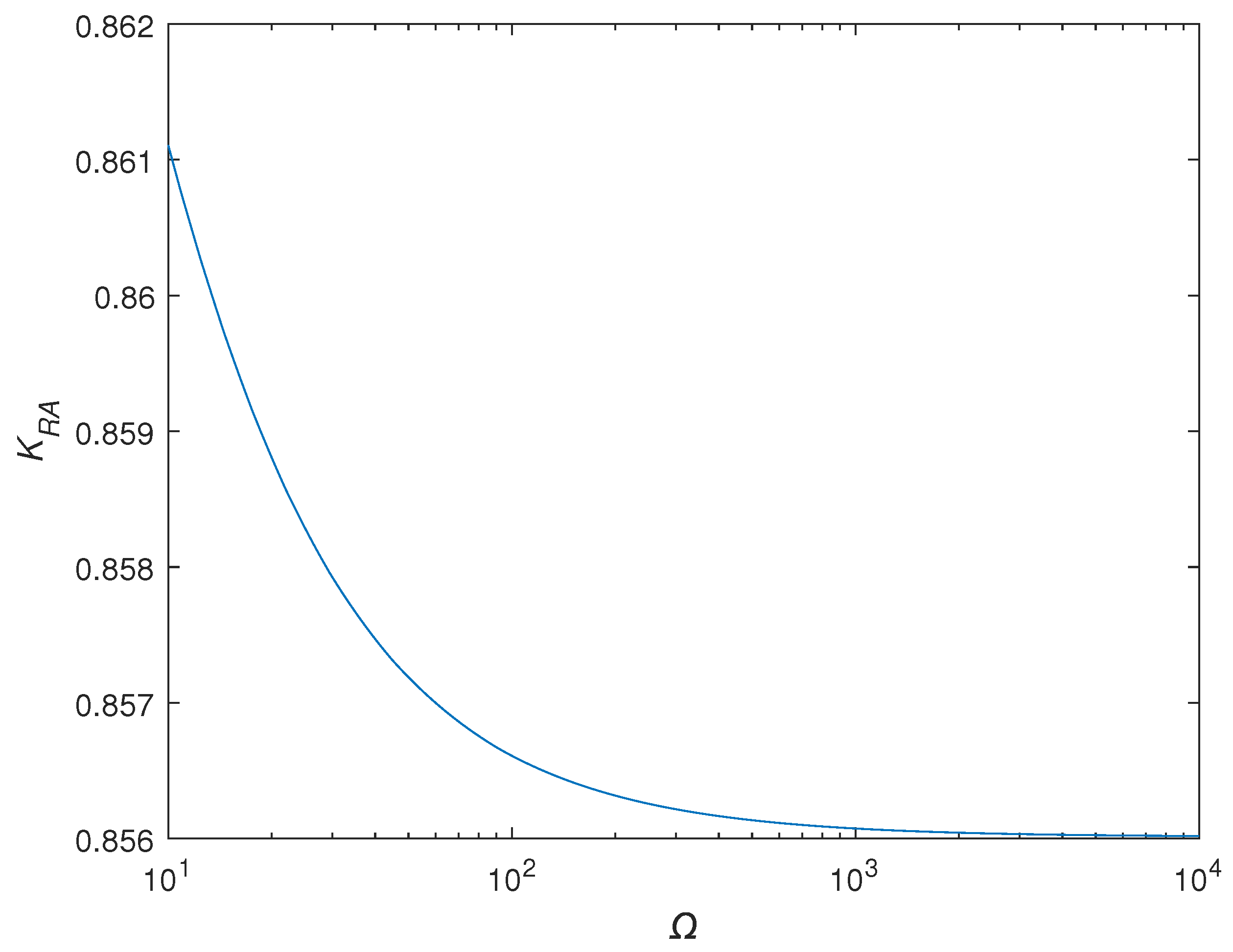
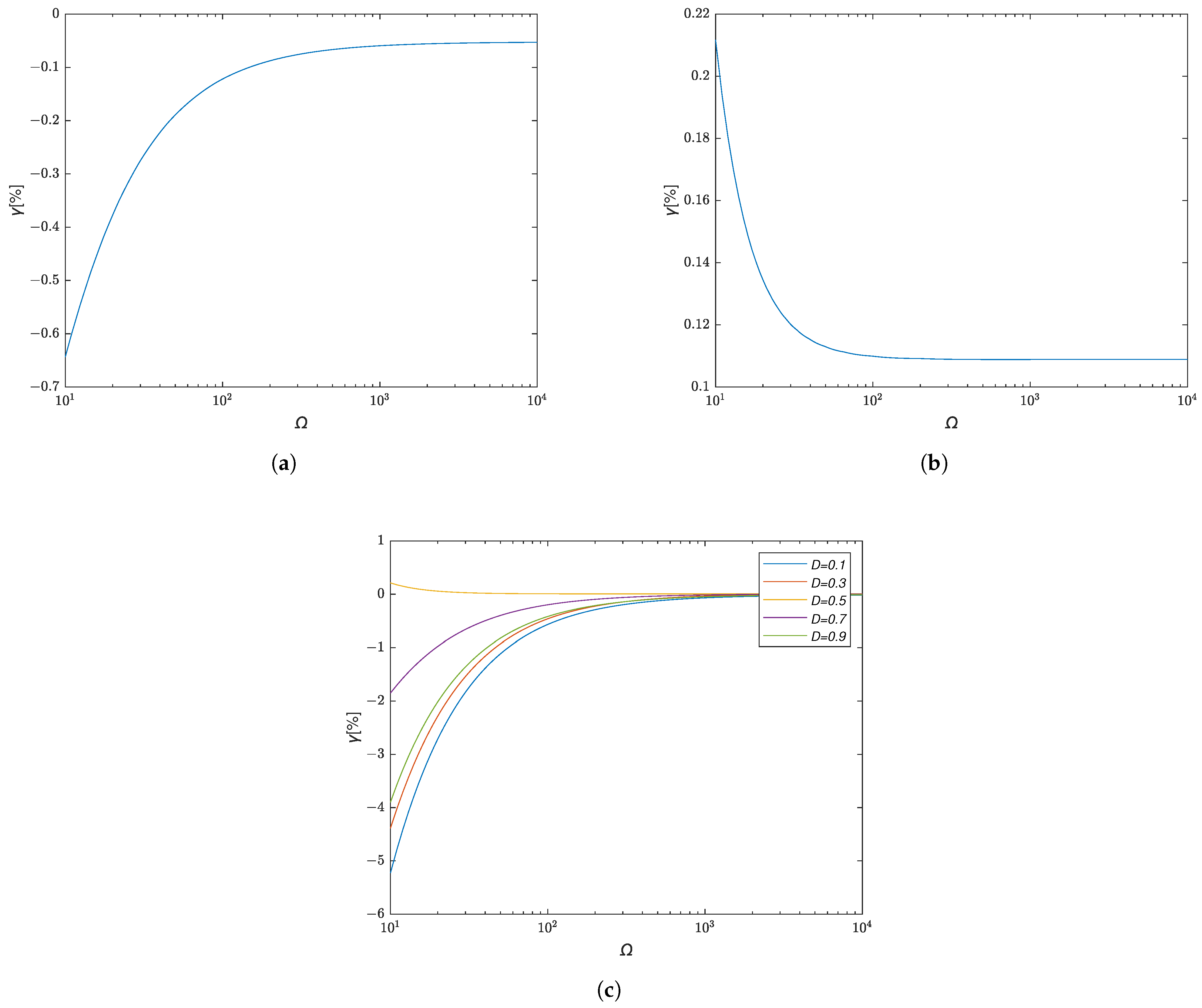
2.2.2. Dynamic Characteristics of Rectified Mean Detection

The rectifier mean-detection circuit in Figure 6 is composed of an absolute value circuit and an average circuit. Its transfer function is simple. The absolutes of the periodic waveforms described in Equations (10)–(12) meet the Dirichlet condition and can be expressed in a time domain via Fourier series [26].
After passing through the absolute value circuit, the sine wave becomes:
x t = A sin ω 0 t
The period of x t is T / 2 and angular frequency is 2 ω 0 . Its Fourier series coefficient is:
a k = 2 T 0 T 2 x ( t ) e j 2 k ω 0 t d t = 2 A 4 π k 2 + π
Thus, its Fourier series is as follows:
x t = k = + a k e j 2 k ω 0 t = k = + 2 A 4 π k 2 + π e j 2 k ω 0 t
To analyze its dynamic characteristics, assume that the input signal is applied from t = 0 . That is x ( t ) = 0 while t < 0 . The complex exponential expression for the absolute of the sine wave is:
x t u t = k = + 2 A 4 π k 2 + π e j 2 k ω 0 t u t
Through Euler’s formula, the trigonometric function expression can be obtained as:
x t u t = 2 A π + k = 1 + 4 A 4 π k 2 + π cos 2 k ω 0 t u t
The complex exponential expression for the absolute of the triangular and periodic pulse wave can also be obtained via by the same transformations as in (20)–(22). For the triangular wave, this is:
x t u t = A 2 + k = + A e j 2 k 1 π 1 π 2 2 k 1 2 e j 2 2 k 1 ω 0 t u t
For periodic pulse wave, it is:
x t u t = A D + k = 1 A sin k D π k π e j k D π e j 2 k ω 0 t + k = 1 + A sin k D π k π e j k D π e j 2 k ω 0 t u t
The trigonometric function expression for the absolute of the triangular wave is further obtained as follows:
x t u t = A 2 + k = 1 + 4 A π 2 2 k 1 2 cos 2 2 k 1 ω 0 t u t
For the periodic pulse wave, it is:
x t u t = A D + k = 1 + 2 A sin k D π k π cos 2 k ω 0 t k D π u t
A finite order of expression is taken; this is Equation (21) changing to x ( t ) = k = N + N a k e j 2 k ω 0 t . The three waveforms are depicted in Equations (23), (26) and (27), as shown in Figure 8.
According to Figure 8, the higher the order of series, the closer its waveform is to the ideal one. While N = 100 , the Fourier series expressions are usually acceptable for representing the original waveforms. For periodic pulse wave, the oscillations occurring at the rising and falling edges are inevitable, which is called the Gibbs phenomenon.
By performing Fourier transform on Equation (22), the frequency domain expression for the absolute of the sine wave can be obtained as:
X j ω = k = + 2 A 4 π k 2 + π 1 j ω 2 k ω 0 + π δ ω 2 k ω 0
The frequency domain expression of the average circuit in Figure 6 is:
H j ω = 1 1 + j ω R C
Thus, the frequency domain expression of the output signal for the sine input is as follows:
Y j ω = X j ω H j ω = 1 1 + j ω R C k = + 2 A 4 π k 2 + π 1 j ω 2 k ω 0 + π δ ω 2 k ω 0
The time domain expression of y ( t ) can be obtained via inverse Fourier transform as:
y t = 2 A π 1 e t R C + k = 1 + 4 A 4 π k 2 + π 1 + 2 R C k ω 0 2 cos 2 k ω 0 t + 2 R C k ω 0 sin 2 k ω 0 t e t R C u t
Similarly, the time-domain expression of y ( t ) for the triangular wave input can be obtained as:
y t = A 2 1 e t R C + k = 1 + 4 A π 2 2 k 1 2 1 1 + 2 R C 2 k 1 ω 0 2 cos 2 2 k 1 ω 0 t + 2 R C 2 k 1 ω 0 sin 2 2 k 1 ω 0 t e t R C u t
The time-domain expression of y ( t ) for periodic pulse input is:
y t = A D 1 e t R C + k = 1 + A sin k D π k π 1 + 2 R C k ω 0 2 4 R C k ω 0 sin k D π 2 cos k D π e t R C cos 2 k ω 0 t + k = 1 + A sin k D π k π 1 + 2 R C k ω 0 2 4 R C k ω 0 cos k D π + 2 sin k D π sin 2 k ω 0 t u t
Take a finite series N = 100 and set the cutoff frequency of the average circuit as f C = 1 / ( 2 π R C ) = 1 Hz. The three output waveforms are depicted through Equations (31)–(33), as shown in Figure 9.
All three Equations (31)–(33) are composed of two parts. One is the first-order step response with a time constant of R C and with amplitude of the rectified mean value. Another is the ripple composed of multi-toned signals. Figure 9 coincides with the above description. In order to ensure that the comparison circuits in Figure 2 and Figure 4 do not repeatedly switch due to a ripple around the comparison threshold, a hysteresis comparison circuit must be used. When the peak to peak value of the ripple V R P P is less than the hysteresis voltage, the repeated switching issue caused by the ripple can be eliminated.
Let the ripple amplitude be V R A = 0.5 V R P P . In order to evaluate the ripple amplitude, Equation (31) can be transformed into:
y ( t ) = 2 A π + k = + 2 A e t R C 4 π k 2 + π 1 + 2 R C k ω 0 2 + k = 1 + 4 A 4 π k 2 + π 1 + 2 R C k ω 0 2 sin 2 k ω 0 t + φ k u t
while φ k = arctan 1 2 R C k ω 0 .
The output waveform is divided into three parts in Equation (34). The first one is DC signal 2 π A , which does not change with time. The second part contains the exponential decay function e t R C , which approaches 0 as time goes on. The third part is composed of multi-toned sine waves, which is the stable contributor of ripple. So the estimation of ripple amplitude is based on the third part. The cutoff angular frequency of the first-order filter is:
ω c = 1 R C
Define the normalized frequency Ω as:
Ω = ω 0 ω c
The third part of Equation (34) can be transformed into:
V R A = max k = 1 + 4 A 4 π k 2 + π 1 + 2 k Ω 2 sin 2 k ω 0 t + φ k 2 A Ω π k = 1 + 1 4 k 2 + 1 k = 2 A Ω π ln 4 1
The estimated value of the ripple amplitude is:
V R A = 2 A Ω π ln 4 1
The estimated value V R A in Equation (38) is simply the sum of amplitudes of all sinusoidal components. It cannot be met while considering the influence of phase values φ k = arctan 1 2 k Ω . The actual ripple amplitude will be smaller. The ratio of ripple amplitude to its estimated value is defined as:
K R A = V R A V R A
Figure 10 shows the relationship between K R A and Ω :
As shown in Figure 10, when Ω continues to increase, K R A approaches a constant 0.856. The minimum value of Ω is set to 10; that is, only the condition when the signal frequency is greater than 10 times the cutoff frequency of the first-order low-pass filter is considered. Other subsequent waveform analyses will also be carried out according to this condition. With the correction constant of 0.856, the ripple amplitude estimation Equation (38) can be rewritten as:
V R A = 0.21 A Ω
For the triangular wave, transformations similar to Equations (34)–(37) are performed on Equation (32) to obtain:
V R A = max k = 1 + 4 A π 2 2 k 1 2 1 + 2 2 k 1 Ω 2 sin 2 2 k 1 ω 0 t + φ k 2 A Ω π 2 k = 1 + 1 2 k 1 3 2 A Ω π 2 × 1.052
while φ k = arctan 1 2 R C 2 k 1 ω 0 .
For the periodic pulse wave, the following can be obtained:
V R A = max k = 1 + 2 A sin k D π k π 1 + 2 k Ω 2 sin 2 k ω 0 t + φ k A Ω π k = 1 + sin k D π k 2 < A Ω π k = 1 + 1 k 2 = π A 6 Ω
while tan φ k = 2 cos k D π 4 R C k ω 0 sin k D π 4 R C k ω 0 cos k D π + 2 sin k D π .
The ripple amplitudes estimated via Equations (41) and (42) are also based on the assumption that all sinusoidal components are maximized at the same time and the influence of phase is ignored. For periodic pulse input, the final approximation of Equation (42) also ignores the effect of duty cycle D. In actual calculation, different values of D have a great impact on ripple estimation. According to the simulation, when Ω is extra high, K R A only depends on D. Figure 11b shows the relationship between K R A and D, while Ω = 10 4 .
From Figure 11a, a correction constant for triangular wave input is obtained as 0.9228. The ripple estimation equation is rewritten as:
V R A = 0.197 A Ω
For periodic pulse wave, the correction value of ripple estimation can be fitted as a quadratic function related to duty cycle: 2.985 D 2 + 2.985 D + 0.00075 . The estimation equation can be rewritten as:
V R A = 0.524 A Ω 2.985 D 2 + 2.985 D + 0.00075
In order to evaluate the accuracy of ripple estimation Equations (40), (43) and (44), the relative error of ripple estimation is defined as:
γ = V R A V R A V R A × 100 %
Figure 12 shows the relative estimation errors for the three waveforms.
As shown in Figure 12, for both sine and triangular waves, the maximum relative errors of estimated ripple amplitude are less than 1%. For periodic pulse waves, the maximum relative errors depend on duty cycle and all are less than 6%. The estimated ripple amplitude would be used for determination of the hysteresis ratio in a comparison circuit. As shown in the results section, the hysteresis ratios must be higher than the ripple ratio to eliminate protection hiccups. The hysteresis ratios could be set as 1.06 times the calculated value to ignore the ripple estimation error. In Equations (40), (43) and (44), the ripple amplitudes are all inversely proportional to the normalized frequency. That means the ripple amplitude is at a maximum while Ω = 10 .
It should be mentioned that the parameter A in Equations (40), (43) and (44) means the peak value of input waveforms, but the hysteresis voltage is calculated based on the rectified mean value of these waveforms. So the transformation between the peak value and the rectified mean value according to Table 1 is necessary. Define ripple ratio R R P as the ratio of estimated ripple amplitude V R A to rectified mean value X R M S . The ripple ratio can be calculated with Equation (46) for sine, triangular and periodic pulse waveforms, respectively, from top to bottom.
R R P = 0.33 Ω 0.394 Ω 0.524 D Ω 2.985 D 2 + 2.985 D + 0.00075
Define hysteresis ratio δ H as the ratio of half the comparator hysteresis voltage to the initial threshold voltage. For these waveforms, if the hysteresis ratio of the comparison circuit is set higher than any ripple ratio calculated via Equation (46) at Ω = 10 , the repeated switching issue could be eliminated.

3. Results

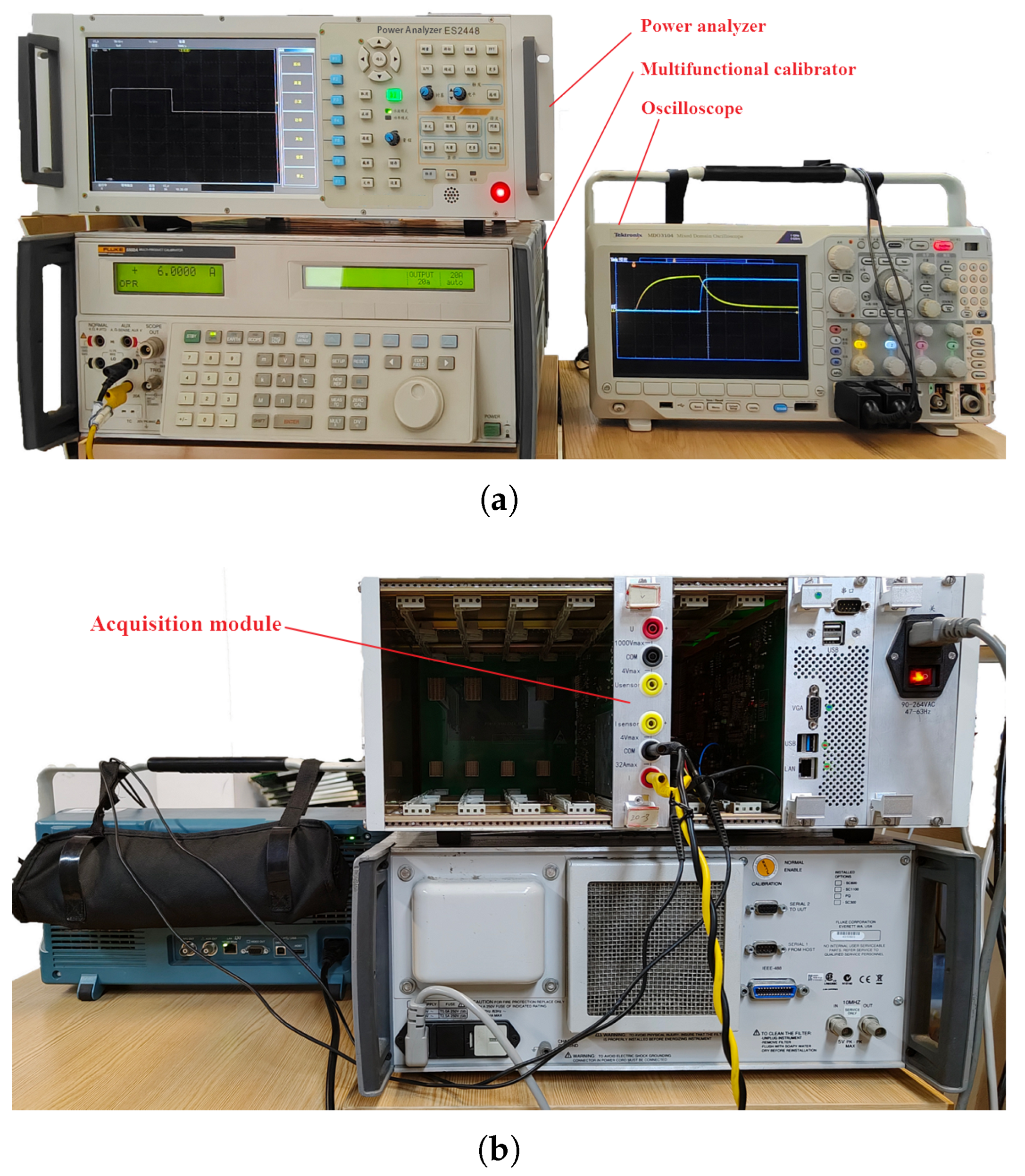
3.1. Experimental Circuit

In order to verify the parallel current-sensing method and its protection circuit, a sensing circuit with five resistors was designed, as shown in Figure 13.
There are two rectified mean-detection circuits and two comparison circuits in Figure 13. Define them as #1 and #2 for the circuits from top to bottom. The resistance values of the five sensing resistors and the current ranges covered are shown in Table 3.
Three current ranges were covered by each sensing resistor. All I R values were effective values. I P K was the peak current covered by each sensing resistor. P R is the rated power consumption for each resistor at the maximum covered current range. The design adopted a unified peak factor of 3. According to the value of the peak current, the maximum range covered by R 1 can be extended to 40 A. Due to the limitation of heat dissipation conditions for the sensing resistor, the maximum range is reduced to 32 A.
In Table 3, the total range (ratio of maximum to minimum range for all resistors) is 1.28 × 10 4 . Similar products that adopted multi sensing resistors in series have total range ratios of 333 and 4000, respectively [15,16]. In contrast, the parallel sensing method has advantages in expanding the dynamic range of current measurement. Through five parallel sensing resistors, the maximum range ratio R R of a single resistor is only 4.167. The large dynamic range requirement of the power analyzer was divided by these sensing resistors. The performance requirements for amplification circuits were decreased. The hardware circuit is shown in Figure 14.
In the hardware circuit, the whole acquisition module is shown and an enlarged image of the current-sensing board is included. Switches S 1 S 5 were achieved through N-channel MOSFETs connected back to back, which have fast switching speed and low power consumption. Three wing-shaped heat sinks had been installed on the circuit board to improve the cooling capacity of the sensing resistors and switches. Two silicon carbide Schottky diodes D 1 and D 2 packaged in TO-247 were applied as the freewheeling diodes. They were installed on an aluminum heat sink on the back side.

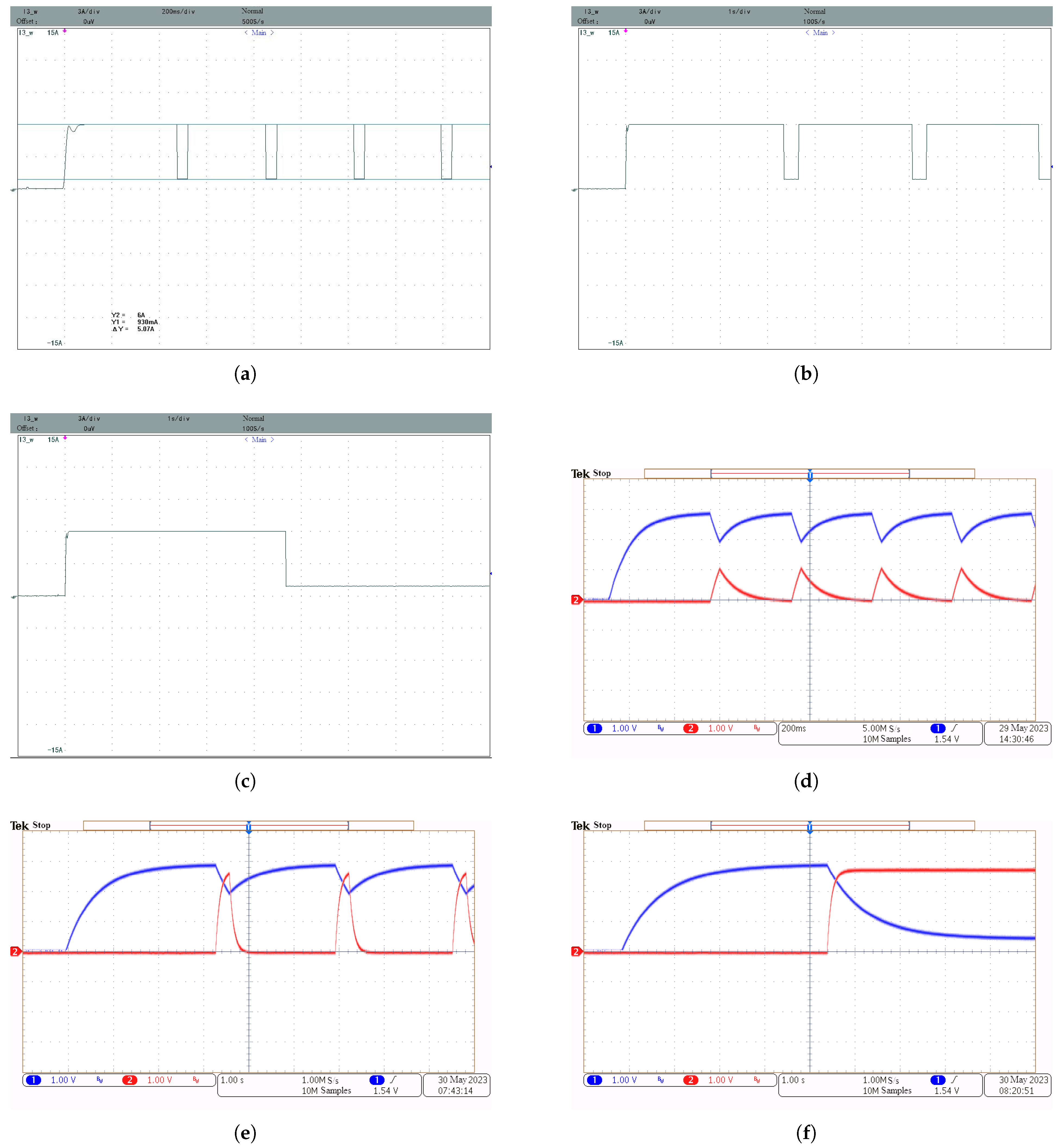
3.2. Time Delay Property of Protection Circuit
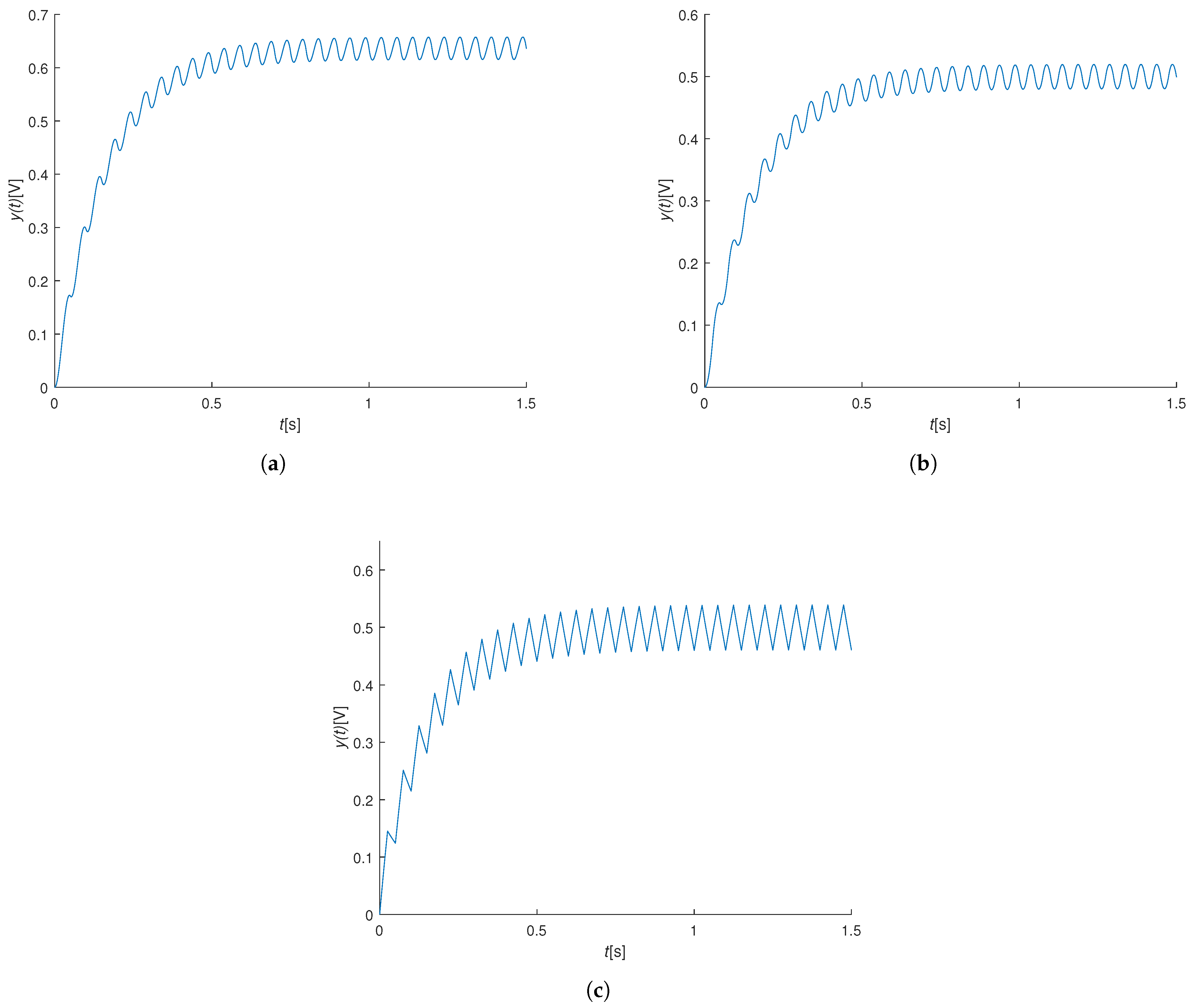
In order to verify the performance of the protection circuit, an experimental platform was built as shown in Figure 15.
The acquisition module was installed in the self-made power analyzer, as shown in Figure 15b. The current waveforms can be displayed on the screen of the power analyzer. A multifunctional calibrator model 5502A provided current input for the current-measurement channel. The output waveforms of rectified mean-detection circuits were captured through the oscilloscope model MDO3104.
The delays of rectified mean-detection circuits in the flow chart of Figure 5 were not considered. When the input current has a step change from a value below the protection threshold I T 2 to a value above, overcurrent protection is generated by closing S 1 . Due to the time delay property of rectified mean-detection circuits, the overcurrent state could not be latched if the time constants or hysteresis ratios were not properly designed.
In order to prevent repetitive switching caused by AC ripple, hysteresis comparison circuits were used in Figure 13. The single supply voltage of the comparators was 4.8 V and the thresholds were set to half the supply voltage V T 1 = V T 2 = 2.4 V. Hence, the hysteresis ratios in both directions of each comparison circuit were the same:
δ H 1 = V T 1 + V T 1 V T 1 = V T 1 V T 1 V T 1 = R I 1 R F 1
where δ H 1 is the hysteresis ratio of the comparison circuit #1; V T 1 + is the positive threshold voltage; V T 1 is the negative threshold voltage.
Similarly, the hysteresis ratio of comparison circuit #2 is:
δ H 2 = R I 2 R F 2
Since all circuits from current sensing to comparator input are linear ones, the hysteresis ratios of current thresholds are the same as the voltage hysteresis ratios mentioned above. One can obtain the following:
I T 1 + = ( 1 + δ H 1 ) I T 1
I T 2 + = ( 1 + δ H 2 ) I T 2
I T 1 = ( 1 δ H 1 ) I T 1
I T 2 = ( 1 δ H 2 ) I T 2
I T 1 + and I T 2 + are the current thresholds flowing through two sensing resistors, while protections are triggered and the outputs of comparators switch from low level to high level.
According to Equation (7), the input current threshold while protection circuit 1 is triggered is:
I T 1 + = I T 1 + ( R S 2 + R 2 + R S 1 + R 1 ) / ( R S 2 + R 2 )
When hysteresis was considered, the hiccup-free condition of the protection process in Figure 5 becomes I T 1 + < I T 2 + . Even if this condition is met, delay of the rectified mean circuit may still cause hiccups.
Let time constants of the first-order filters for two rectified mean circuits be τ 1 and τ 2 , respectively. If both comparator hysteresis and filter delay are considered and the input current I I N is DC, the workflow of the two protection circuits in Figure 13 is as follows:
  • Before the switch S 1 is closed, the currents flowing through the sensing resistor R 1 and R 2 are 0 and I I N , respectively.
  • After the switch is closed, the currents rapidly change to I R 1 and I R 2 , determined by Equations (4) and (5), respectively. Due to a delay of the first-order filter, the changes of output voltages of rectified mean circuits take times. Let the back-calculated currents corresponding to the output voltages be I R 1 and I R 2 , respectively. They are determined by:
    I R 1 ( t ) = I R 1 ( 1 e t τ 1 )
    I R 2 ( t ) = ( I I N I R 2 ) e t τ 2 + I R 2
  • I R 1 gradually increases from 0 to I R 1 and I R 2 gradually decreases from I I N to I R 2 . Make I R 1 ( t 1 ) = I T 1 + and I R 2 ( t 2 ) = I T 2 : At time t 1 , protection circuit 1 enters protection state; At time t 2 , protection circuit 2 exits protection state. To eliminate the hiccup issue in protection circuits, it is necessary to make t 1 < t 2 .
In the experimental circuit, the gains were G 1 = 800 / 3 and G 2 = 24 . It can be calculated that I T 1 = 4.5 A and I T 2 = 5 A. The hysteresis ratios of comparison circuits 1 and 2 were 11% and 19.6%, respectively. One can calculate that I T 1 = 4.005 A, I T 1 + = 4.995 A, I T 2 = 4.02 A, I T 2 + = 5.98 A. When I I N = 6 A, it could be measured via the cursor function of the power analyzer that I R 2 = 0.93 A and I R 1 = 5.07 A, as shown in Figure 16a. In protection circuit 1, let the resistance and capacitance of the first-order low-pass filter be 100 k Ω and 1 μ F, respectively. That is, τ 1 = 100 ms. By setting t 1 = t 2 , the critical point for eliminating hiccups can be calculated as τ 2 = 850 ms, according to Equations (54) and (55). To meet t 1 < t 2 , one should make τ 2 > 850 ms.
The test waveforms are shown in Figure 16.
In Figure 16a, the current acquired via the power analyzer repeatedly switches between 6 A and 0.93 A, indicating the occurrence of protection hiccups. From Figure 16d–f, the red and blue waveforms were rectified mean output V R M 1 and V R M 2 for circuit 1 and 2, respectively. In Figure 16d, during the process of V R M 2 decreasing from the positive comparison threshold of 2.88 V to the negative threshold of 1.92 V, there was no time for V R M 1 to rise to the positive comparison threshold of 2.664 V, resulting in protection hiccups. In Figure 16e, as τ 2 increased, V R M 1 rose higher, but was still lower than 2.664 V. The hiccup still existed, as shown in Figure 16b. In Figure 16f, τ 2 = 880 ms > 850 ms, the protection hiccup was eliminated, as shown in Figure 16c. It should be mentioned that two different time scales are used in Figure 16: In Figure 16a,d, the time scale is 200 ms/div; in Figure 16b,c,e,f, the time scale is 1 s/div.
From the above analysis and tests, it can be concluded that the following conditions should be met to eliminate the protection hiccup:
  • The protection thresholds were set as I T 1 + < I T 2 + ;
  • τ 2 was significantly higher than τ 1 ;
  • Comparison circuit 2 had a high hysteresis ratio.
The above test is based on DC input current. What is the difference if the input is an AC waveform? According to Equations (31)–(33), all outputs of the rectified mean circuits for these three waveforms can be expressed as the combination of first-order step response of rectified mean value and AC ripple. When Ω 10 , the ripple amplitude is much lower than the rectified mean value. The delay issue caused by first-order filters is similar to that of the DC input, with time constants of τ 1 and τ 2 . The conditions for eliminating protection hiccups are the same as for DC input. AC ripple may cause further protection hiccup issues. The hysteresis ratios of comparison circuits need to be considered according to it.
According to Equation (46), while Ω 10 , the ripple ratio is at a maximum at Ω = 10 . The ripple ratios for various waveforms are shown in Table 4.
From Table 4, it can be concluded that as the duty cycle decreases, the ripple ratio for periodic pulse input increases. According to Table 2, the parallel overcurrent protection based on rectified mean detection is more effective while D 1 / 3 . When D < 1 / 3 , peak detection based on ADC sample values takes over the role. In summary, for a protection circuit based on rectified mean detection, the highest ripple ratio is 10.4%, while the input is periodic pulse wave and D = 1 / 3 . In the above tests, the hysteresis ratios of comparison circuits 1 and 2 were set as 11% and 19.6%, respectively, both higher than the maximum ripple ratio 10.4%. Thus the repetitive switching issue caused by the AC ripple was eliminated in comparison circuits. Due to the inability of the calibrator in Figure 15 to output periodic pulse current waveforms, the protection hiccup issue caused by the AC ripple cannot be verified in experiments.

4. Discussion

A new current-sensing method—multi resistors in parallel—was proposed in this article. The new method solved the problem of high heat consumption and large layout space occupation with bypass switches and freewheeling diodes in the series sensing method. The limit on the number of sensing resistors was broken through. Thereby, the dynamic range of a single current-measurement channel is improved. The overcurrent state cannot be latched in the parallel shunt protection circuit, resulting in protection hiccups. A dual threshold-detection circuit was proposed to solve the hiccup issue.
In the protection circuit, rectified mean detection was used to roughly measure the effective value of the input current. Through analysis, it was found that the protection circuit based on rectified mean detection has good protection validity for sine, triangular and periodic pulse wave with duty cycle D 1 / 3 . For periodic pulse wave with duty cycle D < 1 / 3 , the validity is lower than the peak detection. Therefore, a protection scheme combining rectified mean-detection circuit and peak detection based on ADC sample values was proposed.
Due to a delay in the rectified mean-detection circuit, if the time constant of the first-order filter and the hysteresis ratio of the comparison circuit are not properly set, protection hiccups may still appear. In order to obtain the dynamic response characteristics of the rectified mean-detection circuit for common waveforms, such as sine, triangular and periodic pulse waves, the following actions were taken: the absolutes of three waveforms were represented via Fourier series; their frequency domain expressions were then obtained through Fourier transform; after multiplying with the transfer function of the first-order filter, the time-domain expressions of three waveforms passed through the rectified mean circuit were obtained through inverse Fourier transform. All three waveforms can be expressed as the sum of the first-order step response and AC ripple. The first-order step response is similar to that of the DC input and the consideration on the time constant for eliminating the protection hiccup is the same; the AC ripple determines the hysteresis ratio of the comparison circuit. The calculation formulas for estimating the ripple ratio of three waveforms are provided in Equation (46).
In the experimental circuit, 5 sensing resistors were used, covering 15 current ranges from 2.5 mA to 32 A. A total range ratio of 1.28 × 10 4 was achieved. This verified the superiority of multi resistors in the parallel sensing method in improving the measurement dynamic range. The correlation between parameters such as protection threshold, time constant of filter and hysteresis ratio and also the conditions for eliminating hiccups are given in Equations (54) and (55). The test results coincide with theoretical calculations.
In addition to the power analyzer involved in this article, the current-sensing topology with multi resistors in parallel and the overcurrent protection method can be used in any current-sensing application with a large dynamic range requirement. The response characteristics of three common current waveforms as input were analyzed. However, the analysis method is universal and other waveforms can be analyzed through the process provided in the article.

5. Conclusions

The small size and contacting properties of sensing resistors make it simple to expand the measurement dynamic range through multiple sensing components. A current-sensing topology with multi resistors in parallel and its protection circuit were proposed. With the new topology, there is no limit to the number of sensing resistors and that number reached 5 in the experimental circuit. Compared to the counterpart with 2∼3 resistors in series, the advantages of the new topology in expanding the measurement dynamic range are shown. A protection circuit based on dual threshold detection was proposed. By combining appropriate filter time constants and comparing circuit hysteresis ratios, protection hiccups were eliminated. The research content of this article has strong engineering significance and can be applied to any current acquisition application with high dynamic range requirement.

Author Contributions

Conceptualization, X.G. and Z.T.; methodology, X.G.; validation, Z.T. and Y.G.; investigation, Y.G.; writing—original draft preparation, X.G.; writing—review and editing, K.C.; supervision, H.W. All authors have read and agreed to the published version of the manuscript.

Funding

This research was funded by the National Key Research and Development Program of China (Grant No. 2020YFB1711000).

Institutional Review Board Statement

Not applicable.

Informed Consent Statement

Not applicable.

Data Availability Statement

The data presented in this study are available on request from the corresponding authors.

Conflicts of Interest

The authors declare no conflict of interest.

Abbreviations

The following abbreviations are used in this manuscript:
CNCComputerized Numerical Control
DCDirect Current
ACAlternative Current
RMSRoot Mean Square

References

  1. Niakan, H.; Sirat, A.P.; Parkhideh, B. A Novel Reset-Less Rogowski Switch-Current Sensor. IEEE Trans. Power Electron. 2023, 38, 4203–4206. [Google Scholar] [CrossRef]
  2. Constantin, G.; Maroșan, I.A.; Crenganiș, M.; Botez, C.; Gîrjob, C.E.; Biriș, C.M.; Chicea, A.L.; Bârsan, A. Monitoring the Current Provided by a Hall Sensor Integrated in a Drive Wheel Module of a Mobile Robot. Machines 2023, 11, 385. [Google Scholar] [CrossRef]
  3. Mușuroi, C.; Volmer, M.; Oproiu, M.; Neamtu, J.; Helerea, E. Designing a Spintronic Based Magnetoresistive Bridge Sensor for Current Measurement and Low Field Sensing. Electronics 2022, 11, 3888. [Google Scholar] [CrossRef]
  4. Patel, A.; Ferdowsi, M. Current sensing for automotive electronics—A survey. IEEE Trans. Veh. Technol. 2009, 58, 4108–4119. [Google Scholar] [CrossRef]
  5. Aiello, O. Hall-effect current sensors susceptibility to emi: Experimental study. Electronics 2019, 8, 1310. [Google Scholar] [CrossRef] [Green Version]
  6. Rydler, K.E.; Bergsten, T.; Tarasso, V. Determination of phase angle errors of current shunts for wideband power measurement. In Proceedings of the 2012 Conference on Precision Electromagnetic Measurements, Washington, DC, USA, 1–6 July 2012; pp. 284–285. [Google Scholar]
  7. Pogliano, U.; Trinchera, B.; Serazio, D. Wideband digital phase comparator for high current shunts. Metrologia 2012, 49, 349. [Google Scholar] [CrossRef] [Green Version]
  8. Wang, Y.; Chen, K.; Gou, X.; He, R.; Qiu, G. A High-Precision and Wideband Fundamental Frequency Measurement Method for Synchronous Sampling Used in the Power Analyzer. Front. Energy Res. 2021, 9, 652386. [Google Scholar] [CrossRef]
  9. Viciana, E.; Arrabal-Campos, F.M.; Alcayde, A.; Baños, R.; Montoya, F.G. All-in-one three-phase smart meter and power quality analyzer with extended IoT capabilities. Measurement 2023, 206, 112309. [Google Scholar] [CrossRef]
  10. Gao, X.; Zhou, Q. A low consumption DSP based power analyzer. In Proceedings of the the 2014 2nd International Conference on Systems and Informatics (ICSAI 2014), Shanghai, China, 15–17 November 2014; pp. 164–168. [Google Scholar]
  11. Badar, J.; Ali, S.; Munir, H.M.; Bhan, V.; Bukhari, S.S.H.; Ro, J.S. Reconfigurable power quality analyzer applied to hardware-in-loop test bench. Energies 2021, 14, 5134. [Google Scholar] [CrossRef]
  12. Meier, A.K. New standby power targets. Energy Effic. 2019, 12, 175–186. [Google Scholar] [CrossRef] [Green Version]
  13. Gerber, D.L.; Meier, A.; Liou, R.; Hosbach, R. Emerging zero-standby solutions for miscellaneous electric loads and the internet of things. Electronics 2019, 8, 570. [Google Scholar] [CrossRef] [Green Version]
  14. Zhou, L.; Li, F.; Wang, Y.; Wang, L.; Wang, G. A new empirical standby power and auxiliary power model of CNC machine tools. Int. J. Adv. Manuf. Technol. 2022, 120, 3995–4010. [Google Scholar] [CrossRef]
  15. Fluke Corporation. Fluke Norma 4000/5000 High Precision Power Analyzers. 2008. Available online: https://dam-assets.fluke.com/s3fs-public/11259-eng-04-A.pdf?vx.Y6RA6T7Z47QNaNoM5JOpfGAlDXkiV (accessed on 14 June 2023).
  16. Yokogawa Test & Measurement Corporation. WT300E Series Digital Power Meter. 2019. Available online: https://cdn.tmi.yokogawa.com/1/2562/files/BUWT300E-01EN.pdf (accessed on 14 June 2023).
  17. Yokogawa Test & Measurement Corporation. WT1800E Series High Performance Power Analyzers. 2022. Available online: https://cdn.tmi.yokogawa.com/1/2678/files/BUWT1800E-01EN.pdf (accessed on 14 June 2023).
  18. ZHIYUAN Electronics. PA Series Power Analyzer. 2021. Available online: https://www.zlg.cn/data/upload/software/Pa/PA%20Serials%20Power%20Analyzer%20VOL.001.pdf (accessed on 14 June 2023).
  19. Bosco, G.C.; Garcocz, M.; Lind, K.; Pogliano, U.; Rietveld, G.; Tarasso, V.; Voljc, B.; Zachovalová, V.N. Phase comparison of high-current shunts up to 100 kHz. IEEE Trans. Instrum. Meas. 2011, 60, 2359–2365. [Google Scholar] [CrossRef]
  20. Schönecker-Baußmann, M. Reference Load For Power Analyzer Phase Adjustment and Calibration up to 150 Khz. IEEE Trans. Instrum. Meas. 2019, 69, 5058–5063. [Google Scholar] [CrossRef]
  21. Gonçalves, J.T.; Valtchev, S.; Melicio, R.; Gonçalves, A.; Blaabjerg, F. Hybrid three-phase rectifiers with active power factor correction: A systematic review. Electronics 2021, 10, 1520. [Google Scholar] [CrossRef]
  22. Power Integrations. Application Note AN-52 HiperPFS Family Design Guide. 2017. Available online: https://www.powerint.cn/sites/default/files/documents/an52.pdf?download=1 (accessed on 7 July 2023).
  23. Huang, P.Y.; Nagasaki, H.; Shimizu, T. Capacitor characteristics measurement setup by using B–H analyzer in power converters. IEEE Trans. Ind. Appl. 2017, 54, 1602–1613. [Google Scholar] [CrossRef]
  24. Charles, K.; Lew, C. RMS to DC Conversion Application Guide. 1986. Available online: https://www.analog.com/media/en/training-seminars/design-handbooks/RMStoDC_Cover-Section-I.pdf?doc=AD8436.pdf (accessed on 14 June 2023).
  25. Muciek, A.K. A method for precise RMS measurements of periodic signals by reconstruction technique with correction. IEEE Trans. Instrum. Meas. 2007, 56, 513–516. [Google Scholar] [CrossRef]
  26. Oppenheim, A.V.; Willsky, A.S. Signals and Systems. In Discrete Signals and Inverse Problems: An Introduction for Engineers and Scientists; John Wiley & Sons: Hoboken, NJ, USA, 2006. [Google Scholar]
Figure 1. Current channel of power analyzer.
Applsci 13 08382 g001
Figure 2. Two resistors in series current-sensing topology with protection circuit.
Applsci 13 08382 g002
Figure 3. Two resistors in parallel current-sensing topology.
Applsci 13 08382 g003
Figure 4. Protection circuit with dual threshold detection for parallel current-sensing topology.
Applsci 13 08382 g004
Figure 5. Work flow of double threshold-detection protection circuit.
Applsci 13 08382 g005
Figure 6. Rectified mean circuit.
Applsci 13 08382 g006
Figure 7. Three common waveform: (a) Sine. (b) Triangular. (c) Periodic pulse.
Applsci 13 08382 g007
Figure 8. Three waveforms depicted via Fourier series expressions: (a) Sine. (b) Triangular. (c) Periodic pulse.
Applsci 13 08382 g008
Figure 9. The output waveforms for input as: (a) Sine. (b) Triangular. (c) Periodic pulse.
Applsci 13 08382 g009
Figure 10. Ripple estimation accuracy for sine wave.
Applsci 13 08382 g010
Figure 11. Ripple estimation accuracy for: (a) Triangular (depends on Ω ). (b) Periodic pulse (depends on D, while Ω = 10 4 ).
Applsci 13 08382 g011
Figure 12. The relative error of ripple estimation equations for input as: (a) Sine. (b) Triangular. (c) Periodic pulse.
Applsci 13 08382 g012
Figure 13. Experiment circuit with 5 parallel sensing resistors.
Applsci 13 08382 g013
Figure 14. Hardware circuit.
Applsci 13 08382 g014
Figure 15. Experimental platform: (a) Front view. (b) Rear view.
Applsci 13 08382 g015
Figure 16. Measured waveforms: Current waveforms while (a) τ 2 = 100 ms; (b) τ 2 = 680 ms; (c) τ 2 = 880 ms. Output waveforms of rectified mean circuits while (d) τ 2 = 100 ms; (e) τ 2 = 680 ms; (f) τ 2 = 880 ms.
Applsci 13 08382 g016
Table 1. The magnitude of various waveforms.
WaveformD X RMS X RM C F W F e R *
Sine/ A / 2 2 A / π 2 1.1110%
Triangular/ A / 3 A / 2 3 1.155−3.81%
DC/AA1111.1%
PulseD A D A D 1 / D 1 / D 1.111 D 1
1AA1111.1%
0.5 A / 2 A / 2 2 2 −21.4%
0.1 A / 1 0 A / 10 10 10 −64.9%
* Defined in Equation (16).
Table 2. The actual protection threshold of various waveforms.
WaveformD X RMS X PK X RM e PK * e RM *
Sine/ V 0 2 V 0 0.9 V 0 112%11.1%
Triangular/ V 0 3 V 0 0.866 V 0 73.2%15.5%
DC/ V 0 V 0 V 0 200%0%
PulseD V 0 V 0 / D D V 0 3 D 1 1 / D 1
1 V 0 V 0 V 0 200%0%
0.5 V 0 2 V 0 V 0 / 2 112%41.4%
1/3 V 0 3 V 0 V 0 / 3 73.2%73.2%
1/9 V 0 3 V 0 V 0 / 3 0%200%
0.1 V 0 10 V 0 V 0 / 10 −5%216%
* Defined in Equations (17) and (18).
Table 3. The sensing resistors and current ranges.
ResistorValue ( Ω ) I R (A) R R I PK (A) P R (W)
R 1 0.00210/20/323.21202.048
R 2 0.021.2/2.5/54.167150.5
R 3 0.10.15/0.3/0.641.80.036
R 4 0.50.02/0.04/0.0840.240.0032
R 5 20.0025/0.005/0.0140.030.0002
Table 4. Ripple ratios of waveforms.
WaveformDuty CycleRipple Ratio
Sine/3.3%
Triangular/3.94%
Pulse0.91.57%
0.74.7%
0.57.83%
1/310.4%
0.311.0%
0.114.1%
Disclaimer/Publisher’s Note: The statements, opinions and data contained in all publications are solely those of the individual author(s) and contributor(s) and not of MDPI and/or the editor(s). MDPI and/or the editor(s) disclaim responsibility for any injury to people or property resulting from any ideas, methods, instructions or products referred to in the content.

