Article

Design of Dual-Notch-Filter-Based Controllers for Enhancing the Dynamic Response of Universal Single-Phase Grid-Connected Power Converters

Applied Energy Laboratory, School of Electrical and Computer Engineering, Ben-Gurion University of the Negev, Beer-Sheva 8410501, Israel
*
Author to whom correspondence should be addressed.
Appl. Sci. 2023, 13(18), 10144; https://doi.org/10.3390/app131810144
Submission received: 8 August 2023 / Revised: 3 September 2023 / Accepted: 7 September 2023 / Published: 8 September 2023
(This article belongs to the Special Issue Innovative Technologies in Power Electronics Converters)

Abstract

:
Trade-off between transient response and grid-side current quality is a well-known issue of single-phase mains-connected power converters. A dual-loop control structure (usually based on PI or type-II controllers) is typically employed in such systems to regulate the DC link voltage to a constant reference (in order to maintain power balance) while forcing the grid-side current to have a specific shape (in order to comply with power quality requirements). Introducing notch term/s (tuned to certain multiple/s of the mains base frequency) into one of the loops allows either for the improvement of the dynamic performance without worsening the total harmonic distortion of grid-side current or for the enhancement of the current quality without impairing the dynamic response. Since the maximum tolerable value of total harmonic distortion is typically imposed by a certain power quality standard, it is desirable to enhance the transient response of the power converter system as much as possible while keeping the total harmonic distortion at the maximum allowed value. However, universal off-grid operating power conversion systems must support both 50 Hz and 60 Hz mains; consequently, tuning the notch term/s to 50 Hz multiple/s would not be sufficient for a 60 Hz mains operation and vice-versa. Consequently, this work examines the possibility of introducing a dual-notch term into the control loop in order to cover both above-mentioned base frequencies. It is demonstrated that under typical base frequency uncertainty values, the performances of dual-notch terms are nearly decoupled so that the term tuned to a 50 Hz frequency (and optionally to its multiples) has nearly no influence at a 60 Hz mains operation and vice-versa. Consequently, the methodology allows for the improvement of the dynamics of universal grid-connected power converters without total harmonic distortion (THD) deterioration. A stability analysis of the proposed control structure is carried out and quantitative design guidelines, allowing for the attainment of an optimized dynamic response for a given maximum tolerable total harmonic distortion, minimum allowed phase margin and a certain base frequency uncertainty, are established. It is shown that a DC link voltage loop bandwidth of 52 Hz may be attained while keeping the grid-side current THD below 5%. Simulations and experimental results support well the proposed design methodology.

1. Introduction

Mains-interfacing power conversion systems are typically obliged by power quality standards to interchange sinusoidal-shaped current with the utility grid [1,2,3]. As a result, alternating instantaneous power is exchanged between the two entities, formed by a DC component and a power component pulsating at twice the mains base frequency [4,5,6]. While the DC component is transferred to/from the load/source in order to carry the energy, the pulsating power constituent should not be allowed to reach the load/source to avoid lifetime reduction and excessive losses [7,8,9]. Consequently, DC link capacitors are typically employed to compensate instantaneous power mismatch between grid-side and load/source-side both in steady state and during transients [10,11,12]. This is accomplished by regulating the average DC link capacitor voltage (reflecting the stored energy) to a constant reference value employing a PI or type-2 compensator [13,14,15,16] without counteracting the pulsating power component. As a result, pulsating current flows through the DC link capacitor, giving rise to an uncontrolled DC link voltage ripple [17,18], which is proportional to the total power processed and inversely proportional to the DC link capacitance value and DC link voltage reference value [19,20]. Upon sensing the DC link voltage and feeding it back to the regulation loop, the ripple distorts the grid-side current magnitude reference signal (created by the loop compensator), leading to an increased total harmonic distortion (THD) of utility-side current [21,22]. In order to limit the THD, the gain of DC link voltage loop compensator should be restricted in the vicinity of double the base utility frequency [23], implying a trade-off between AC-side current THD and DC link voltage dynamics in case compensators with monotonically decreasing frequency response characteristics (e.g., PI or type-2) are employed [24,25,26]. Typically, around 10 Hz DC link voltage loop bandwidth is attained under 5% grid-side current THD restriction. Such a relatively low bandwidth imposes a high value of the required DC link capacitance in order to cope with sharp load-side power variations, since the DC link voltage value should always remain above the maximum of grid-side voltage to retain converter controllability [22,24].
Many solutions aiming to improve the trade-off have been suggested. Utilizing line voltage and/or load current feedforward to compensate against parameter variations does not increase the DC voltage loop bandwidth, yet it requires additional sensors [27,28,29,30]. The ripple estimation and cancellation techniques proposed in [31,32,33,34,35,36] indicated an improved performance, yet requiring a relatively complex circuitry and a significantly increased computational burden. The implementation of approaches based on nonlinear and/or time-varying control proposed in [37,38,39,40] call for a high-performance microcontroller. On the other hand, linear filtering-based methods proposed in [41,42,43,44,45,46,47] seem to be much simpler in terms of analysis and implementation. In particular, compensators combining a PI or type-II term with a notch filter may be easily realized either digitally or by a simple analog network. As mentioned above, the value of DC link voltage loop gain should be restricted in the vicinity of double the base utility frequency in order to limit the THD. A notch filter was combined with the current loop controller in [48] to enhance transient responses at both the DC bus voltage and the output current. Introducing a notch filter tuned to double the mains base frequency allows for local DC-link voltage loop gain minimization without restricting the corresponding PI or type-II controller gain, thus attaining an increased crossover frequency. Disturbance observer-based approaches, employing notch terms, were shown to yield a similar effect [49,50]. Design guidelines for obtaining PI + Notch controller coefficients based on the maximum tolerable grid-side current THD and transient DC link voltage deviation were established in [51].
Nevertheless, neither of the above-mentioned notch-filter-based solutions took into account the fact that a universal grid-connected converter must be capable of supporting both 50 Hz and 60 Hz grid frequencies. Moreover, utilizing transient DC link voltage deviation may yield non-optimal performance in terms of phase margin “overkill”. Recently, a disturbance observer-based approach [50] was extended to employ dual-notch-based action in [52], yet the methodology may only be applied to existing systems with slow PI or type-II controllers and cannot be employed in from-scratch designs. In addition, the control structures of disturbance observer-based methods are quite complex and not easy to implement.
Consequently, the main contributions of this work are as follows:
1.
It is suggested to combine a PI term with two notch filters, tuned to 50 Hz and 60 Hz, respectively, in order to support universal grid interfacing without the need for controller redesign.
2.
The minimum allowed phase margin is used as the second performance merit (along with the maximum tolerable grid-side current THD) rather than the maximum tolerable transient DC link voltage deviation. Such an approach allows the optimization of the latter rather than setting a desired value a priori (which may lead to a non-existing solution, requiring further iterations).
An explicit process of deriving coefficients of the proposed PI + N2 controller employed for regulating the DC-link voltage of single-phase converters interfacing either 50 Hz or 60 Hz mains is proposed in this work. The proposed methodology allows for the optimization of the DC-link voltage transient caused by step-like load changes while attaining prescribed values of grid-side current THD and DC-link voltage loop phase margin under the prescribed mains frequency uncertainty range.
The rest of the paper is organized as follows. The essentials of single-phase grid-connected power conversion system operation are brought forward in Section 2. The steady-state performance of the system in terms of total harmonic distortion and its dynamic response in terms of DC-link voltage deviation upon step-like load variation are revealed analytically in Section 3 and Section 4, respectively. Guidelines for the proposed controller coefficient derivation are established in Section 5. The simulations and experiments of the proposed methodology applied to a 500 W grid-connected converter are demonstrated in Section 6. The paper is then concluded in Section 7.

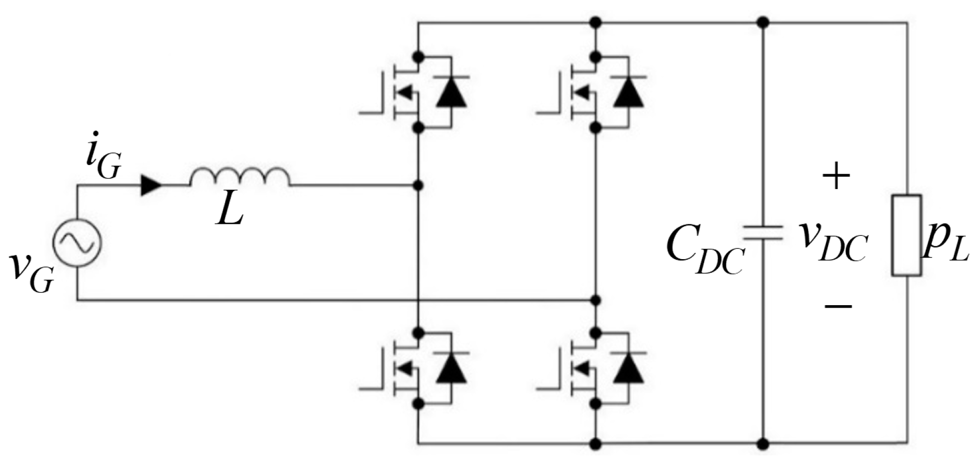
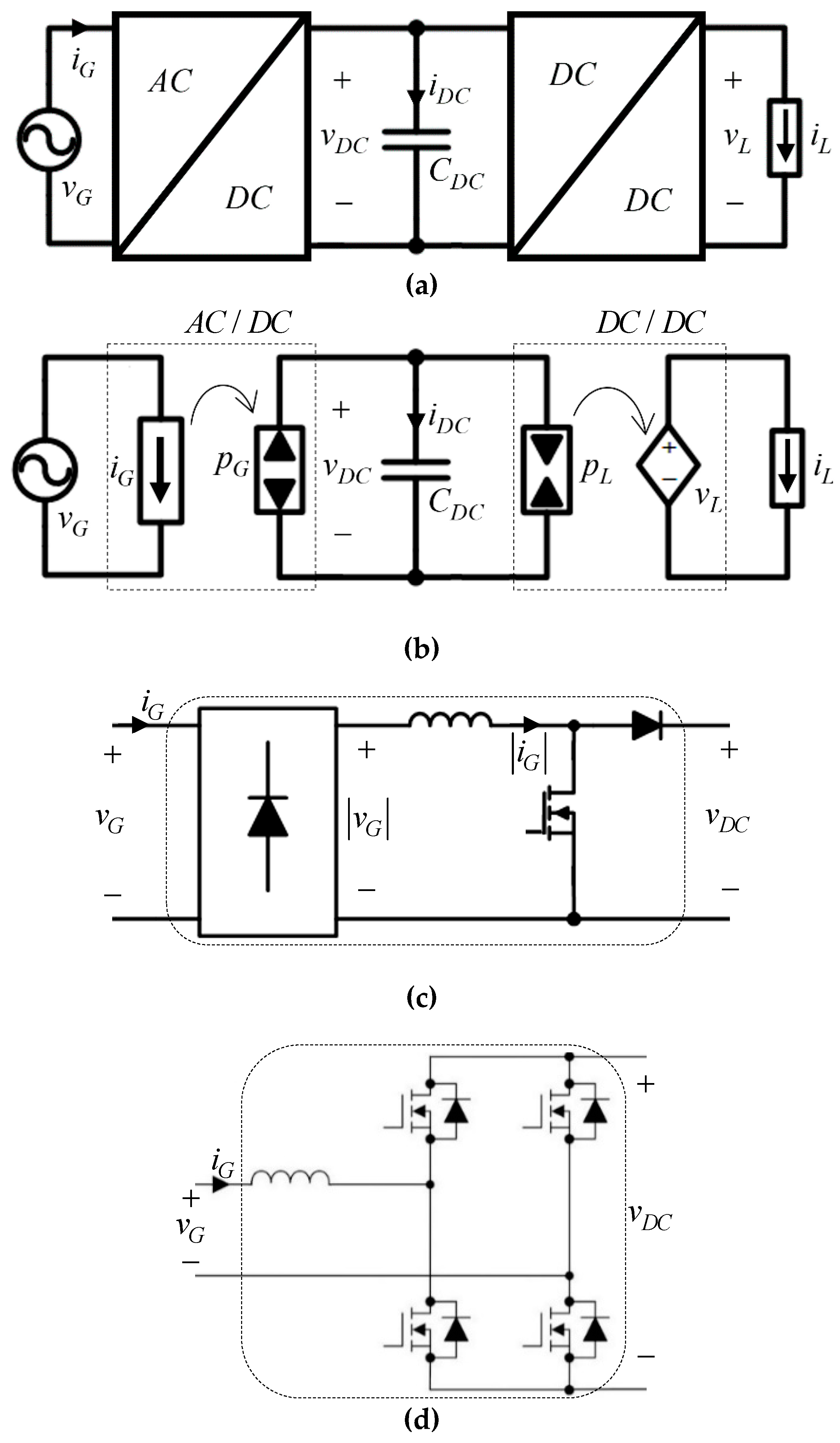
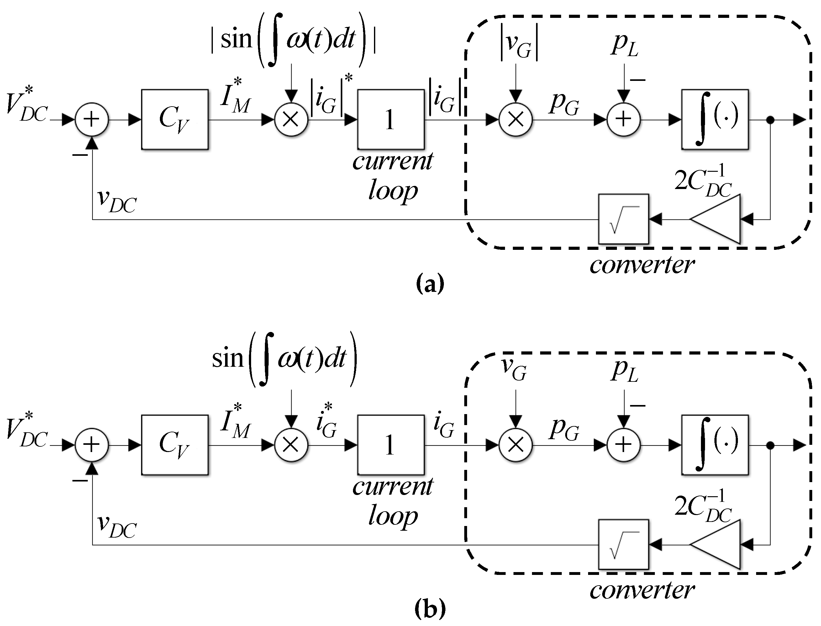
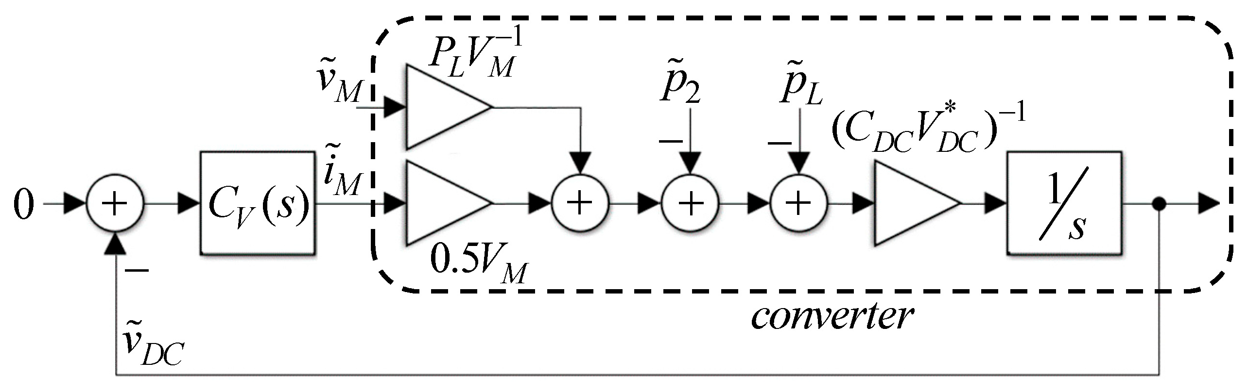
2. Single-Phase Grid-Connected Power Conversion System

Consider a typical dual-stage off-grid operating power conversion system depicted in Figure 1a, formed by a mains-interfacing AC/DC converter and a downstream DC-DC converter, interconnected via a DC link capacitance CDC. The grid is assumed to act as energy source in the subsequent discussion, yet the methodology remains valid in case the energy flows from the DC side to the AC side. Moreover, all the variables below are switching-cycle-average, i.e., free from switching components. Considering harmonic-free mains and unity power factor operation for brevity (yet without loss of generality), the grid-side voltage and current are given by [52]
v G ( t ) = v M ( t ) sin ω ( t ) d t , i G ( t ) = i M ( t ) sin ω ( t ) d t
with ω denoting the instantaneous base frequency of the grid and vM, iM representing the corresponding magnitudes. In steady state, the above quantities are constant so that
v M ( t ) = V M , i M ( t ) = I M , ω ( t ) = ω G .
In steady state, the base frequency of the mains may attain the following values,
ω G = α 100 π , 50 Hz m a i n s 120 π , 60 Hz   m a i n s
with α [αmin < 1, αmax > 1] representing the corresponding deviation from nominal values (i.e., |1 − α| indicates the corresponding uncertainty). On the other hand, DC-side variables are also constant in steady state so that
v L ( t ) = V L , i L ( t ) = I L .
Assuming lossless conversion, a functional diagram of the power conversion system is shown in Figure 1b with
p L ( t ) = v L ( t ) i L ( t ) , p G ( t ) = v G ( t ) i G ( t ) , v D C ( t ) i D C ( t ) = p G ( t ) p L ( t ) ,
where vDC(t) and iDC(t) represent the voltage across the DC link capacitance CDC and the corresponding current, respectively. Combining (1) with (5) yields [10]
v D C ( t ) i D C ( t ) = v D C ( t ) C D C d v D C ( t ) d t i D C ( t ) = 0.5 v M ( t ) i M ( t ) 0.5 v M ( t ) i M ( t ) cos 2 ω ( t ) d t v L ( t ) i L ( t ) ,
reducing in steady state to
C D C v D C s s ( t ) d v D C s s ( t ) d t = 0.5 V M I M 0.5 V M I M cos 2 ω G t V L I L ,
which may be split into
0.5 V M I M = V L I L
and
C D C v D C s s ( t ) d v D C s s ( t ) d t = 0.5 V M I M cos 2 ω G t ,
respectively. Consequently, the steady-state expressions of grid-side current and DC link voltage are given by
I M = 2 P L V M , P L = V L I L
and
v D C s s ( t ) = V D C * 1 P L ω G V D C * 2 C D C sin 2 ω G t ,
respectively, with V D C * denoting the DC link voltage set point value. In practice,
P L ω G V D C * 2 C D C < < 1
typically holds; hence, (11) may be further reduced to [11]
v D C s s ( t ) V D C * Δ v D C ( t ) , Δ v D C ( t ) = Δ V D C sin 2 ω G t , Δ V D C = P L 2 ω G V D C * C D C .
Consequently, steady-state DC link voltage would always be formed by the dominating DC component and the significantly smaller double-base-frequency pulsating ripple component, proportional to the load power and inversely proportional to the DC link capacitance, DC link voltage set point, and base frequency of the mains.
It must be emphasized that two typical realizations of the grid-interfacing AC/DC converter exist in practice. In case of unidirectional AC-to-DC power conversion, a grid-interfacing converter is often realized by a diode bridge rectifier followed by a boost DC-DC converter, as shown in Figure 1c. In case of DC-to-AC energy flow, the grid-interfacing converter operates as an inverter and should be realized in a bridgeless manner, e.g., as shown in Figure 1d. It should be mentioned, however, that unidirectional rectifiers may also be realized by bridgeless topology circuits. The corresponding control structures are depicted in Figure 2. In case a bridge-rectifier-based topology is utilized, all the measurements are taken at the DC side of the converter. The outer (voltage) loop regulates the DC link voltage by feeding the difference between the corresponding set point V D C * and the measured value vDC into the voltage controller CV, which calculates the mains current magnitude value I M * required to maintain the power balance (cf. (10)). On the other hand, the rectified mains voltage v G is sensed and the corresponding unity magnitude template s i n ω ( t ) d t is extracted and multiplied by I M * in order to generate the reference signal for the rectified grid-side current i G * . The inner (current) loop regulates the rectified grid-side current by feeding the difference between the corresponding reference i G * and the measured value i G into the current controller CI, which calculates the required modulating signal. The output of the PWM modulator is then fed to the switch of the boost DC-DC converter (cf. Figure 1c).
In case a bridgeless topology is utilized, grid-side measurements are required. While the outer (voltage) loop is similar to that of the bridge-rectifier-based topology, here the mains voltage vG is sensed and the corresponding unity magnitude template s i n ω ( t ) d t is extracted and multiplied by I M * in order to generate the reference signal for the grid-side current i G * . The inner (current) loop regulates the grid-side current by feeding the difference between the corresponding reference i G * and the measured value iG into the current controller CI, which calculates the required modulating signal. The outputs of the PWM modulator are then fed to the switches of the AC/DC converter (cf. Figure 1d).
It was shown in [53] that the attainable bandwidth ωCI of a typical current loop is given by
ω C I 0.5 π P M I * T d ,
where P M I * is the desired phase margin of the current loop and Td is the total switching and sampling delay, the worst case of which equals 1.5 times the sampling period. Considering the typical values of P M I * = π 4 and switching frequency of 50 kHz, the attainable current loop bandwidth would be 2 π · 4167 rad/s, which is about two decades higher than the attainable voltage loop bandwidth. Consequently, it may be assumed that
i G ( t ) = i G * ( t ) , i G ( t ) = i G ( t ) *
with a high degree of accuracy. Noticing that
v G ( t ) i G ( t ) = v G ( t ) i G ( t ) = p G ( t ) .
holds for (1) and combining (15) with (6) while taking Figure 1b and Figure 2 into account, the corresponding simplified closed-loop system representations are depicted in Figure 3 [51].
In this paper, the controller CV is realized by a cascaded proportional-integral–dual-notch (PI + N2) structure
C V ( s ) = K τ s + 1 s P I ( s ) s 2 + 200 π 2 s 2 + 2 ξ f 200 π s + 200 π 2 N F 1 ( s ) s 2 + 240 π 2 s 2 + 2 ξ f 240 π s + 240 π 2 N F 2 ( s ) N 2 ( s )
with 0 ≤ ξf ≤ 1, proposed by the authors in [54]. There are three parameters to be determined (namely K, τ and ξf) according to the desired phase margin of the voltage loop P M V * , the maximum tolerable total harmonic distortion value THD* and the expected deviation of base frequencies from their nominal values α.

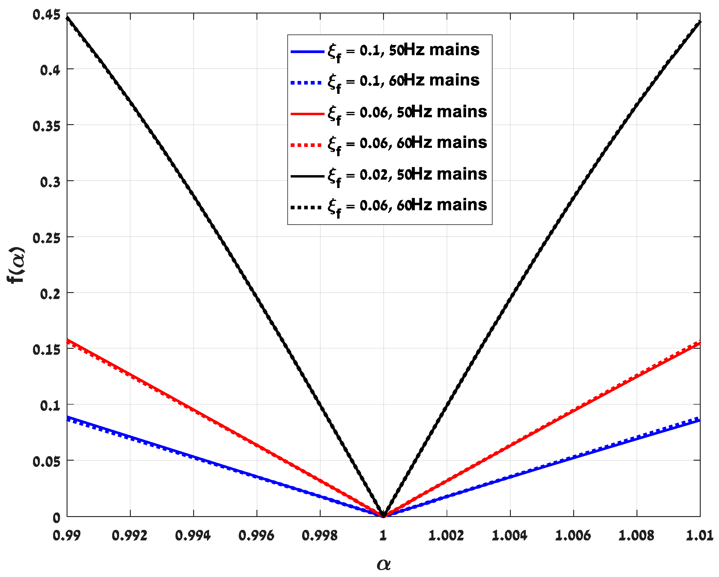
3. Total Harmonic Distortion

According to (10), (13) and Figure 3, there is
I M * = 2 P L V M Δ V D C C V 2 ω G sin 2 ω G t + arg C V 2 ω G
in steady state. Consequently (cf. (15)), there is
i G ( t ) = I M * sin ω G t = 2 P L V M 1 V M Δ V D C 2 P L C V 2 ω G sin 2 ω G t + arg C V 2 ω G sin ω G t
in case of a diode bridge-based rectifier. If
V M Δ V D C 2 P L C V 2 ω G < < 1
then (19) implies grid current [51]
i G ( t ) = 2 P L V M 1 V M Δ V D C 2 P L C V 2 ω G sin 2 ω G t + arg C V 2 ω G sin ω G t = 2 P L V M sin ω G t + V M Δ V D C 4 P L C V 2 ω G cos ω G t + arg C V 2 ω G V M Δ V D C 4 P L C V 2 ω G sin 3 ω G t + arg C V 2 ω G ,
formed by the first and the third harmonic components only. Note that (21) also holds in the case of bridgeless grid-interfacing converter implementation. Consequently, the grid-side current THD is given by (cf. (20))
T H D V M Δ V D C 4 P L C V 2 ω G .
Furthermore, (20) may be reformulated as
2 T H D < < 1 ,
which is typically true since THD values of 5% and below are typically considered. Hence, (20) is justified and (21) is a valid approximation.
It may be concluded from (21) that the pulsating ripple component of the DC link voltage (13) imposes a non-zero grid-side current THD. Denoting the maximum tolerable THD value as THD*, the combination of (13) and (21) yields the following constraint
V M 8 ω G V D C * C D C C V 2 ω G = T H D * C V 2 ω G = 4 2 ω G V D C * C D C V M T H D * ,
which must be satisfied within the region given by the following union (cf. (3))
2 α min 100 π 2 ω G 2 α max 100 π 2 α min 120 π 2 ω G 2 α max 120 π .
Considering (23) with (17) yields
K 2 ω G τ 2 + 1 2 ω G × 200 π 2 2 ω G 2 200 π 2 2 ω G 2 2 + 4 ω G ξ f 200 π 2 240 π 2 2 ω G 2 240 π 2 2 ω G 2 2 + 4 ω G ξ f 240 π 2 = 4 2 ω G V D C * C D C V M T H D * .
Combining (26) with (3) leads to
K 2 ω G τ 2 + 1 2 ω G × 1 1 + 4 ξ f 2 α 2 1 α 2 2 1 1 + 4 ξ f 2 5 6 α 2 1 5 6 α 2 2 = 4 2 ω G V D C * C D C V M T H D * , ω G = α 100 π K 2 ω G τ 2 + 1 2 ω G × 1 1 + 4 ξ f 2 α 2 1 α 2 2 1 1 + 4 ξ f 2 6 5 α 2 1 6 5 α 2 2 = 4 2 ω G V D C * C D C V M T H D * , ω G = α 120 π
unified as
K 2 ω G τ 2 + 1 2 ω G f α = 4 2 ω G V D C * C D C V M T H D *
with
f α = 1 1 + 4 ξ f 2 α 2 1 α 2 2 1 1 + 4 ξ f 2 5 6 α 2 1 5 6 α 2 2 , ω G = α 100 π 1 1 + 4 ξ f 2 6 5 α 2 1 6 5 α 2 2 , ω G = α 120 π
denoting the multiplication of tuned and un-tuned notch term gains, respectively. Plots of f(α) versus 0.99 ≤ α ≤ 1.01 (signifying 1% mains frequency uncertainty) are depicted in Figure 4 for different values of ξf. As expected, the gain of the notch term is zero at nominal frequency (theoretically implying THD = 0), increasing with detuning. Moreover, the highest total f(α) is attained at αmin for 50 Hz mains and at αmax for 60 Hz mains. Nevertheless, since the magnitude response of the PI term in (17) monotonically decreases until the effect zero begins to kick in, the gain at ωG = αmin∙100π may be expected as the worst case one. In addition, it is well-evident that increasing ξf improves robustness to frequency variations. It should be emphasized that if ξf = 0 is selected, the control structure in (17) reduces to the typical PI regulator.

4. Dynamic Response

Reformulating (6) as
C D C v D C ( t ) d v D C ( t ) d t = 0.5 v M ( t ) i M ( t ) p L ( t ) 0.5 v M ( t ) i M ( t ) cos 2 ω ( t ) d t p 2 ( t )
and linearizing around the operating point by substituting
v D C ( t ) = V D C * + v ˜ D C ( t ) , i M ( t ) = 2 P L V M + i ˜ M ( t ) , v M ( t ) = V M + v ˜ M ( t ) , p L ( t ) = P L + p ˜ L ( t ) , p 2 ( t ) = P L cos 2 ω G t + p ˜ 2 ( t ) ,
into (31) and neglecting high-order small-signal terms yields
C D C V D C * d v ˜ D C ( t ) d t = 0.5 V M i ˜ M ( t ) + P L V M v ˜ M ( t ) p ˜ L ( t ) p ˜ 2 ( t ) .
The resultant control structure is depicted in Figure 5 [22].
The corresponding loop gain is obtained as
L ( s ) = 0.5 V M C D C V D C * s C V ( s ) =                               0.5 V M K C D C V D C * τ s + 1 s 2 s 2 + 200 π 2 s 2 + 2 ξ f 200 π s + 200 π 2 s 2 + 240 π 2 s 2 + 2 ξ f 240 π s + 240 π 2 =                               ω n 2 2 ξ n ω n s + 1 s 2 N F 1 ( s ) N F 2 ( s ) ,           ω n = 0.5 K V M C D C V D C * ,             ξ n = ω n τ 2 .
Denoting the crossover frequency of the voltage loop as ωCV, the corresponding phase and gain contributions of the notch terms are given by
arg N F 1 ( ω C V ) = tan 1 2 ξ f 200 π ω C V ω C V 200 π , arg N F 2 ( ω C V ) = tan 1 2 ξ f 240 π ω C V ω C V 240 π , N F 1 ( ω C V ) = 1 1 + 4 ξ f 2 200 π ω C V ω C V 200 π 2 , N F 2 ( ω C V ) = 1 1 + 4 ξ f 2 240 π ω C V ω C V 240 π 2 ,
respectively. The Bode diagram of dual-notch term NF1(s)∙NF2(s) is depicted in Figure 6 for different values of ξf and ω < 200π (since ωCV < 200π in practice). It is well-evident that increasing the value of ξf escalates both the phase and gain contributions of the dual-notch term.
It is well-evident that the gain contribution may be neglected within the whole frequency range considered, thus
L ( ω C V )   ω n 2 ω C V 2 2 ξ n ω C V ω n + 1 = 1
should be satisfied at the crossover frequency ωCV, yielding the crossover frequency
ω C V = ξ n 2 + 2 1 + 1 4 ξ n 4 θ n ω n = θ n ω n .
On the other hand, the phase contribution in (34) must be taken into account, imposing
arg L ( ω C V ) = t g 1 2 ξ n ω C V ω n tan 1 2 ξ f 200 π ω C V ω C V 200 π tan 1 2 ξ f 240 π ω C V ω C V 240 π π = π + P M V *
at the crossover frequency with P M V * indicating the desired voltage loop phase margin. Solving (37) with (36), there is
ξ n = t g P M V * + β 2 2 4 2 t g P M V * + β 2 2 2 + 1 4 1 4 , β = tan 1 2 ξ f 200 π ω C V ω C V 200 π + tan 1 2 ξ f 240 π ω C V ω C V 240 π .
Note that β in (38) may be approximated for simplicity (with some safety margin) as
β 2 tan 1 2 ξ f 200 π ω C V ω C V 200 π ,
hence, in order to minimize it, ξ f should satisfy
ξ f < < 1 2 200 π ω C V ω C V 200 π .
Setting ξ f to
ξ f = 1 2 λ 200 π ω C V ω C V 200 π ,
and substituting into (39), there is
β 2 tan 1 λ 2 λ , λ < < 1 .
In order to bound β by βmax degrees, λ should be set to
λ = 1 2 tan β max
and P M V * increased by βmax degrees to compensate for β. For the value of βmax = 5° recommended in [51], λ = 0.0437 should be selected. In case ξ f is bounded according to (40), ξ n and θ n are presented graphically versus the typical range of the desired voltage loop phase margin values in Figure 7 and Figure 8, respectively. It may be concluded that both parameters increase with the rise in P M V * . In addition, the crossover frequency ωCV is always higher than ωn for the practical values of the desired voltage loop phase margin.
In practice, the variations of grid voltage magnitude and frequency are slower with respect to the voltage loop time constant. Consequently, a critical transient response is the one caused by load power variations. The corresponding transfer function of interest may be derived from Figure 5 (neglecting the influence of the dual notch term) as
v ˜ D C ( s ) p ˜ L ( s ) p 2 ( t ) = 0 G n s s 2 + 2 ξ n ω n s + ω n 2 , G n = 1 C D C V D C * .
Therefore, the load power step of ΔPL imposes a DC link voltage perturbation expressed as
v ˜ D C ( s ) p 2 ( s ) = 0 = G n Δ P L s 2 + 2 ξ n ω n s + ω n 2 v ˜ D C ( t ) p 2 ( t ) = 0 = G n Δ P L ω n 1 ξ n 2 e ξ n ω n t sin ω n 1 ξ n 2 t .
On the other hand, the contribution of p2(t) is given by ΔvDC(t) in (13). Consequently, the total DC link voltage deviation may be approximated by
v ˜ D C ( t ) = v ˜ D C ( t ) p 2 ( t ) = 0 + Δ v D C ( t ) = G n Δ P L ω n 1 ξ n 2 e ξ n ω n t sin ω n 1 ξ n 2 t Δ P L 2 ω G V D C * C D C sin 2 ω G t ,
bounded by
v ˜ D C ( t ) = v D C ( t ) V D C * max v ˜ D C ( t ) p 2 ( t ) = 0 + max Δ v D C ( t ) = Δ P L V D C * C D C 1 ω n e ξ n cos 1 ξ n 1 ξ n 2 + 1 2 ω G .
Since the value of ξ n is dictated solely by P M V * + β max (cf. (38)), the total DC link voltage deviation is reduced when ω n is increased. Since ω n is proportional to ωCV (cf. (37)) for a given P M V * , increasing ω n is equivalent to increasing the voltage loop bandwidth. Moreover, the right-hand side within the brackets of (46) implies that ωG = αmin∙100π would also be the worst case in terms of contribution to the DC link voltage deviation. It should be recalled that in an earlier work [51], the desired undershoot value rather than the minimal tolerable phase margin was used as a performance merit, yielding excessive stability at the expense of a larger DC link voltage overshoot. Here, a minimal tolerable phase margin is imposed, yielding an improved DC link voltage undershoot, as shown next.

5. Controller Parameters Selection

Combining (28) with (33) and solving while considering the worst-case grid frequency ωG = αmin∙100π yields
ω n = 8 ξ n α min 100 π 1 + T H D * 2 ξ n 4 f 2 α min 1 .
with
f α min = 1 1 + 4 ξ f 2 α min 2 1 α min 2 2 1 1 + 4 ξ f 2 5 6 α min 2 1 5 6 α min 2 2 .
As mentioned at the end of the preceding section, ω n should be maximized in order to optimize the transient response (i.e., minimize the DC link voltage deviation). According to (43), this implies minimizing the value of f(α) since ξ n is dictated solely by P M V *   + βmax. However, this conclusion contradicts the one drawn in Section 3, where the opposite was required in order to improve the steady-state performance. Consequently, the trade-off between steady-state and dynamic performances remains and the proposed methodology aims to improve it but not eliminate it. According to (36) and (48), the crossover frequency is then given by
ω C V = θ n 8 ξ n α min 100 π 1 + T H D * 2 ξ n 4 f 2 α min 1 .
Substituting (50) into (41) and rearranging, there is
ξ f = 1 2 λ 1 θ n 2 ξ n α min 1 + T H D * 2 ξ n 4 f 2 α min 1 θ n 2 ξ n α min 1 + T H D * 2 ξ n 4 f 2 α min 1 .
Since θ n and ξ n are known from (36) and (38), solving (51) with (49) yields the value of ξ f . Then, ω n is obtained from (48) and the coefficients of the PI controller term in (17) are obtained as (cf. (33))
K = 2 C D C V D C * V M ω n 2 , τ = 2 ξ n ω n .
The proposed process of controller coefficient tuning is then summarized as follows:
1.
Initialize βmax and   P M V * .
2.
Obtain θ n using (36), ξn using (38) and λ using (43).
3.
Initialize THD* and αmin.
4.
Obtain ξf using (51) and ωn using (48).
5.
Initialize VM, CDC and V D C * .
6.
Determine K and τ using (52).
7.
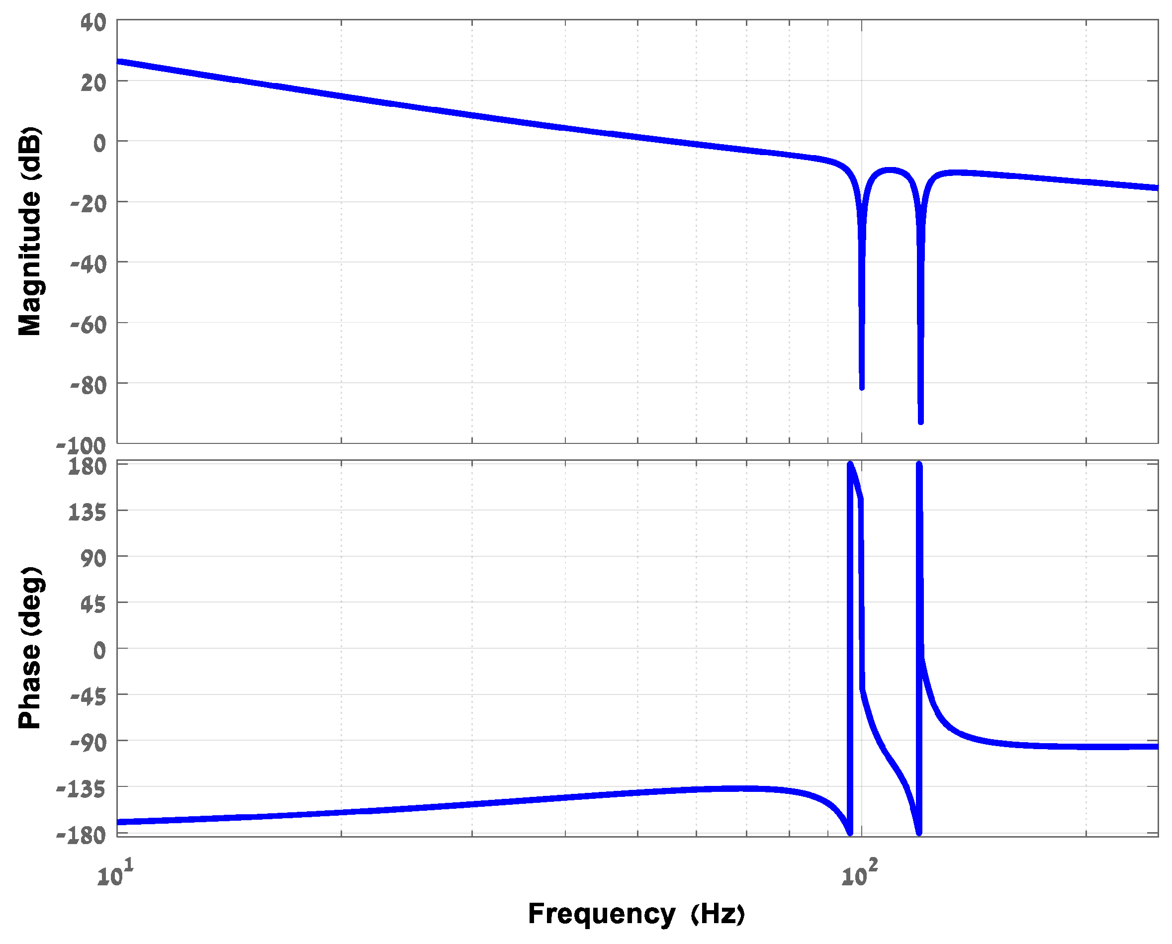
Verify the design by Bode diagram.
8.
Release requirement/s and iterate if necessary.

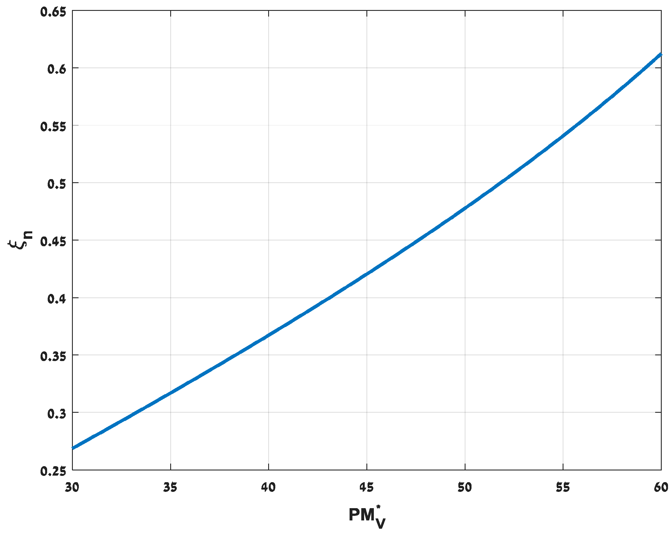
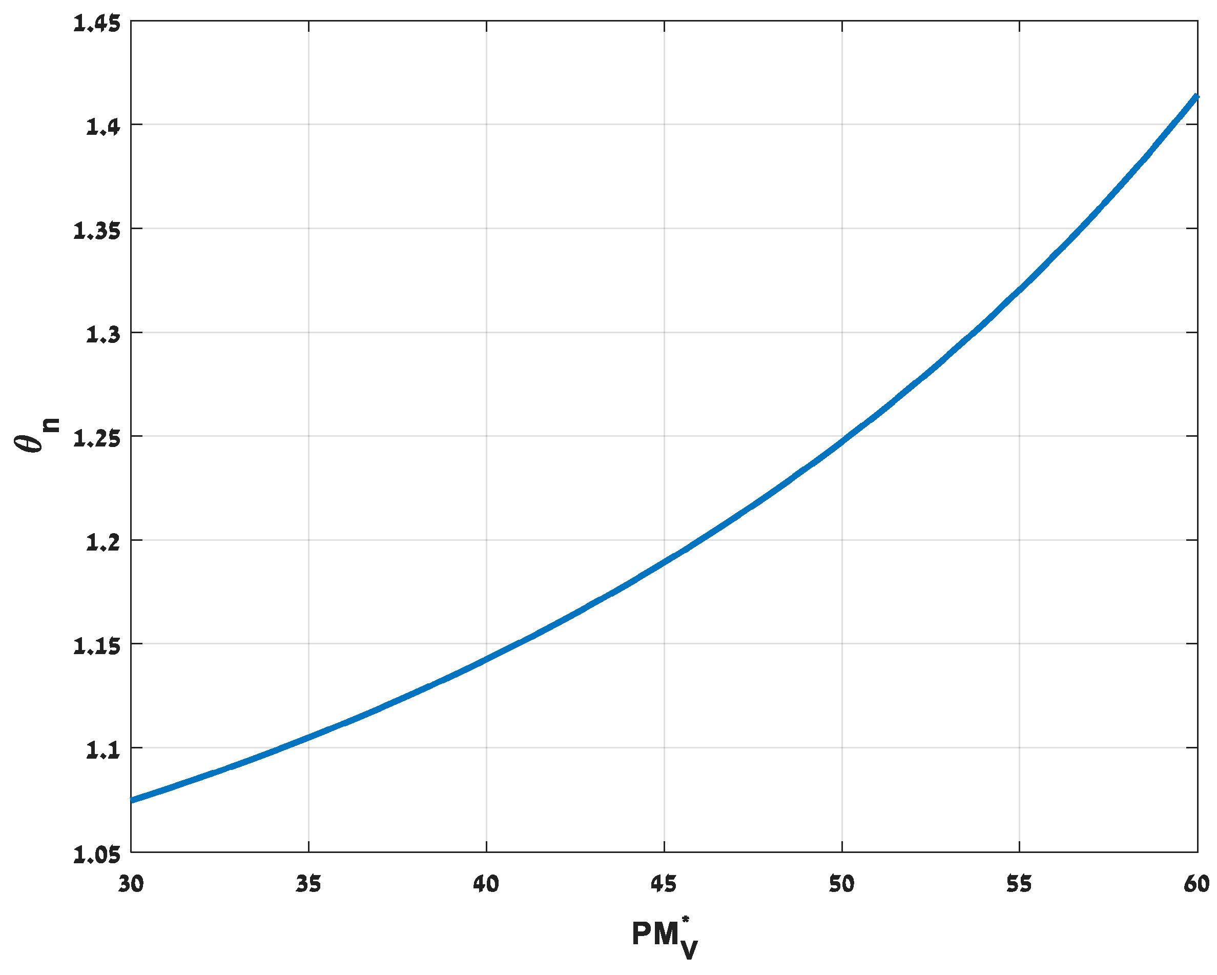
6. Example and Validation

Consider a bidirectional 500 W single-phase grid-connected converter shown in Figure 9 (the downstream DC-DC converter is represented by the power load element pL [55]) operating at a switching frequency of 30 kHz with L = 3.5 mH. The value of the DC link capacitance was set to C D C = 385   μ F [22] and the DC link voltage set point was selected as V D C * = 400   V [51]. The desired performance merit pair was selected as THD* = 0.05, P M V * = 40°. The grid frequency uncertainty was assumed to be 1%, i.e., α  [αmin = 0.99, αmax = 1.01] were considered for both 50 Hz and 60 Hz mains and the corresponding magnitude was set to VM = 325 V. According to the process of controller coefficient tuning proposed in the previous section:
1.
β = 7.5° and P M V * = 40° + 7.5°.
2.
θ n = 1.2, ξn = 0.45 and λ = 0.066.
3.
THD* = 0.05 and αmin = 0.99.
4.
ξf = 0.047 and ωn = 2π∙45 rad/s.
5.
VM = 325 V, CDC = 385   μ F and V D C * = 400 V.
6.
K = 76 and τ = 0.0032.
Figure 9. Grid-interfacing converter under study.
Applsci 13 10144 g009
The resulting Bode diagram of the DC link voltage loop gain (cf. (33)) is depicted in Figure 10, indicating a crossover frequency of ωCV = 2π∙52 rad/s and a phase margin of 39.2° in accurate agreement with P M V * = 40°.
It is interesting to compare the expected performance to the one demonstrated in [51]. Here, voltage deviation of ~10 V is expected (cf. (47)) under a 40° phase margin. On the other hand, a DC link deviation of 20 V was attained in [51] under a 58° phase margin. It may be then concluded that imposing a minimal tolerable phase margin yields an optimized DC link voltage deviation, as stated at the end of Section 4.

6.1. Simulations

During simulations (PSIM 2022 software), the transient responses of the DC link voltage and grid-side current to a zero-to-rated power step-like load variation, and the corresponding steady-state performance under the proposed control methodology were evaluated. The results are depicted in Figure 11 and Figure 12 for 50 Hz and 60 Hz mains, respectively.
It may be concluded that the system operates as expected under the proposed methodology in terms of dynamic response (a ~10 V DC link voltage deviation is evident irrespectively of mains frequency). As to the grid-side current quality, Table 1 summarizes the corresponding steady-state THD values. It is evident that the system designed according to the proposed approach complies well with THD* at ωG = αmin∙100π. Moreover, the THD attains near-zero values at the nominal values of the mains frequency, as predicted above.

6.2. Experiments

In order to validate the proposed methodology experimentally, a modified Texas Instruments High Voltage Single Phase Inverter Kit [56] (Figure 13) was utilized.
The control algorithm was realized adopting first-order hold digitization [57] by a TMS320F28335 DSP-based control card under an average-current-controlled inner loop. The utility was emulated by an APS-7100 Gw Instek programmable AC power source operating as 50 Hz/60 Hz ±   1 % , 230Vrms sinusoidal voltage source. The M9715B Maynuo DC electronic load functioning in constant power mode was employed to emulate the power load pL (cf. Figure 9).
During the simulation framework, it was shown that frequency variations have a negligible influence on the shape of transient responses; hence, the latter were recorded for nominal mains frequency values only. The corresponding results are depicted in Figure 14, matching well the corresponding simulation results demonstrating ~10 V DC link deviations upon a step-like load variation.
The steady-state performance under a rated load around 50 Hz and 60 Hz mains is demonstrated in Figure 15 and Figure 16, respectively. Prior to the experimental framework, the AC power source voltage THD was measured and found to be 0.5%, as shown in Figure 9 in [22]. This value should be taken into account in order to correctly interpret the measured values of THDi. Table 2 summarizes the corresponding steady-state THD values. It is evident that the system designed according to the proposed approach complies well with THD*.

7. Conclusions

A method for deriving the coefficients of a proportional-integral and dual-notch controller employed for regulating the DC link voltage of single-phase converters interfacing either 50 Hz or 60 Hz mains was proposed in this work. The suggested approach allows for the optimization of the DC link voltage transient caused by step-like load changes while attaining the prescribed values of the grid-side current total harmonic distortion and the DC link voltage loop phase margin under a certain uncertainty range of mains frequency. An explicit process of controller coefficient tuning was established and successfully validated both by simulations and experimentally. It was shown that the 50 Hz and 60 Hz notch terms are nearly decoupled in frequency domain, allowing the proposed methodology to attain an approximate 5-fold increase in the DC link voltage loop crossover frequency compared to the classical PI control under a 5% grid-side current THD restriction, a 45° phase margin and a 1% grid frequency uncertainty. Future work on the subject will focus on distorted grid interfacing (calling for multi-dual-notch-based control structure) and examining the advantages of replacing the PI term of the controller with a type-II regulator. It is expected that the additional degree of freedom inherent in the type-II regulator may further improve the trade-off between steady-state and transient converter behavior. Moreover, multi-dual-notch-based control structures may give rise to stability issues which must be identified and appropriately resolved.

Author Contributions

Conceptualization, S.B. and A.K.; methodology, P.S. and A.K.; validation, S.B. and P.S.; formal analysis, A.K.; investigation, S.B. and P.S.; resources, A.K.; writing—original draft preparation, S.B.; writing—review and editing, A.K.; supervision, A.K.; project administration, A.K.; funding acquisition, A.K. All authors have read and agreed to the published version of the manuscript.

Funding

This research was funded in part by the Israel Science Foundation, grant number 2186/19, and by the Israel Innovation Authority.

Institutional Review Board Statement

Not applicable.

Informed Consent Statement

Not applicable.

Data Availability Statement

No new data were created or analyzed in this study. Data sharing is not applicable to this article.

Conflicts of Interest

The authors declare no conflict of interest.

References

  1. Zha, X.; Huang, M.; Liu, Y.; Tian, Z. An overview on safe operation of grid-connected converters from resilience perspective: Analysis and design. Int. J. Electr. Power Energy Syst. 2022, 143, 108511. [Google Scholar] [CrossRef]
  2. Taul, M.G.; Wang, X.; Davari, P.; Blaabjerg, F. Current reference generation based on next-generation grid code requirements of grid-tied converters during asymmetrical faults. IEEE J. Emerg. Sel. Top. Power Electron. 2020, 8, 3784–3797. [Google Scholar] [CrossRef]
  3. Liu, Y.; Li, L.; Shan, P.; Yu, H.; Zhang, S.; Huang, M.; Liu, W.; You, X.; Zhang, P.; Sun, Y.; et al. Coordinated mitigation control for wideband harmonic of the photovoltaic grid-connected inverter. Appl. Sci. 2023, 13, 7441. [Google Scholar] [CrossRef]
  4. Castellan, S.; Buja, G.; Menis, R. Single-phase power line conditioning with unity power factor under distorted utility voltage. Int. J. Electr. Power Energy Syst. 2020, 121, 106057. [Google Scholar] [CrossRef]
  5. Gazafrudi, S.M.M.; Langerudy, A.T.; Fuchs, E.F.; Al-Haddad, K. Power quality issues in railway electrification: A comprehensive perspective. IEEE Trans. Ind. Electron. 2015, 62, 3081–3090. [Google Scholar] [CrossRef]
  6. Awad, H.; Ibrahim, A.M.; De Santis, M.; Bayoumi, E.H.E. Unity power factor operation in microgrid applications using fuzzy type 2 nested controllers. Appl. Sci. 2023, 13, 5537. [Google Scholar] [CrossRef]
  7. Li, X.; Zhang, W.; Li, H.; Xie, R.; Chen, M.; Shen, G.; Xu, D. Power management unit with its control for a three-phase fuel cell power system without large electrolytic ca-pacitors. IEEE Trans. Power Electron. 2011, 26, 3766–3777. [Google Scholar] [CrossRef]
  8. Baek, J.-B.; Choi, W.-I.; Cho, B.-H. Digital adaptive frequency modulation for bidirectional DC–DC converter. IEEE Trans. Ind. Electron. 2013, 60, 5167–5176. [Google Scholar] [CrossRef]
  9. Wen, H.; Xiao, W.; Wen, X.; Armstrong, P. Analysis and evaluation of DC-Link capacitors for high-power-density electric vehicle drive systems. IEEE Trans. Veh. Technol. 2012, 61, 2950–2964. [Google Scholar] [CrossRef]
  10. Mellincovsky, M.; Yuhimenko, V.; Peretz, M.M.; Kuperman, A. Low-frequency DC-link ripple elimination in power converters with reduced capacitance by multi-resonant direct voltage regulation. IEEE Trans. Ind. Electron. 2017, 64, 2015–2023. [Google Scholar] [CrossRef]
  11. Strajnikov, P.; Peretz, M.M.; Kuperman, A. Reduced-rating-electronic-capacitor-based DC links for power electronics sup-ported distributed energy resources. IEEE Trans. Smart Grid 2022, 13, 3943–3953. [Google Scholar] [CrossRef]
  12. Wang, H.; Wang, H.; Zhu, G.; Blaabjerg, F. An overview of capacitive DC links topology derivation and scalability analysis. IEEE Trans. Power Electron. 2020, 35, 1805–1829. [Google Scholar] [CrossRef]
  13. Cheikh-Mohamad, S.; Celik, B.; Sechilariu, M.; Locment, F. PV-Powered Charging Station with Energy Cost Optimization via V2G Services. Appl. Sci. 2023, 13, 5627. [Google Scholar] [CrossRef]
  14. Khajehoddin, S.A.; Karimi-Ghartemani, M.; Jain, P.K.; Bakhshai, A. DC-Bus Design and control for a single-phase grid-connected renewable converter with a small energy storage component. IEEE Trans. Power Electron. 2013, 28, 3245–3254. [Google Scholar] [CrossRef]
  15. Mallik, A.; Lu, J.; Khaligh, A. Notice of Removal: A Comparative study between PI and Type-II compensators for H-bridge PFC converter. IEEE Trans. Ind. Appl. 2018, 54, 1128–1135. [Google Scholar] [CrossRef]
  16. Nabatirad, M.; Razzaghi, R.; Bahrani, B. Autonomous power balance in hybrid AC/DC microgrids. Int. J. Electr. Power Energy Syst. 2023, 146, 108752. [Google Scholar] [CrossRef]
  17. Mellincovsky, M.; Yuhimenko, V.; Peretz, M.M.; Kuperman, A. Analysis and control of direct voltage regulated active DC-link capacitance reduction circuit. IEEE Trans. Power Electron. 2018, 33, 6318–6332. [Google Scholar] [CrossRef]
  18. Mellincovsky, M.; Yuhimenko, V.; Zhong, Q.-C.; Peretz, M.M.; Kuperman, A. Active DC link capacitance reduction in grid-connected power conversion systems by direct voltage regulation. IEEE Access 2018, 6, 18163–18173. [Google Scholar] [CrossRef]
  19. Liu, B.; Song, D.; He, D.; Song, S.; Yang, J.; Su, M.; Lu, Y.; Chen, Y.; Liu, H. A modified modulation for single-phase photovoltaic/battery inverter to improve AC power quality with low DC-link capacitance. Int. J. Electr. Power Energy Syst. 2019, 110, 705–712. [Google Scholar] [CrossRef]
  20. Mutovkin, A.; Yuhimenko, V.; Mellincovsky, M.; Schacham, S.; Kuperman, A. Control of direct voltage regulated active DC-link capacitance reduction circuits to allow plug-and-play operation. IEEE Trans. Ind. Electron. 2019, 66, 6527–6537. [Google Scholar] [CrossRef]
  21. Merai, M.; Naouar, M.; Slama-Belkhodja, I.; Monmasson, E. A systematic design methodology for DC-link voltage control of single phase grid-tied PV systems. Math. Comput. Simul. 2021, 183, 158–170. [Google Scholar] [CrossRef]
  22. Strajnikov, P.; Kuperman, A. Guidelines for voltage controller coefficients design to attain prescribed grid current THD and DC-link voltage undershoot values in power factor correction front ends. IEEE J. Emerg. Sel. Top. Power Electron. 2022, 10, 6523–6533. [Google Scholar] [CrossRef]
  23. Kuperman, A. On the explicit relation between mains-side current THD and DC link voltage controller gain in grid-connected converters. In Proceedings of the 2022 IEEE 26th International Conference on Intelligent Engineering Systems (INES), Georgioupolis Chania, Greece, 12–15 August 2022; IEEE: Piscataway, NJ, USA, 2022; pp. 000069–000072. [Google Scholar] [CrossRef]
  24. Sebastián, J.; Lamar, D.G.; Rodríguez-Alonso, A.; de Azpeitia, M.A.P.; Gonzalez, A.F. On the maximum bandwidth attainable by power factor correctors with a standard compensator. IEEE Trans. Ind. Appl. 2010, 46, 1485–1497. [Google Scholar] [CrossRef]
  25. Mutovkin, A.; Mellincovsky, M.; Yuhimenko, V.; Schacham, S.; Kuperman, A. Conditions for direct applicability of electronic capacitors to dual-stage grid-connected power conversion systems. IEEE J. Emerg. Sel. Top. Power Electron. 2019, 7, 1805–1814. [Google Scholar] [CrossRef]
  26. Zarei, S.F.; Mokhtari, H.; Ghasemi, M.A.; Peyghami, S.; Davari, P.; Blaabjerg, F. DC-link loop bandwidth selection strategy for grid-connected inverters considering power quality requirements. Int. J. Electr. Power Energy Syst. 2020, 119, 105879. [Google Scholar] [CrossRef]
  27. Ghosh, R.; Narayanan, G. Generalized feed-forward control of single phase PWM rectifiers using disturbance observes. IEEE Trans. Ind. Electron. 2007, 54, 984–993. [Google Scholar] [CrossRef]
  28. Figures, E.; Benavent, J.M.; Garcera, G.; Pascual, M. A control circuit with load-current injection for single-phase pow-er-factor-correction rectifiers. IEEE Trans. Ind. Electron. 2007, 54, 1272–1282. [Google Scholar] [CrossRef]
  29. Yao, K.; Wu, C.; Chen, J.; Yang, J.; Li, J.; Jin, Z.; Wang, S.; Yang, R.; Liu, L.; Gao, Y.; et al. A Scheme to improve power factor and dynamic response performance for CRM/DCM Buck–Buck/Boost PFC converter. IEEE Trans. Power Electron. 2021, 36, 1828–1843. [Google Scholar] [CrossRef]
  30. Chiang, H.C.; Lin, F.J.; Chang, J.K.; Chen, K.F.; Chen, Y.L.; Liu, K.C. Control method for improving the response of single-phase continuous conduction mode boost power factor correction rectifier. IET Power Electron. 2016, 9, 1792–1800. [Google Scholar] [CrossRef]
  31. Pena-Alzola, R.; Bianchi, M.A.; Ordonez, M. Control Design of a PFC with Harmonic mitigation function for small hybrid AC/DC buildings. IEEE Trans. Power Electron. 2016, 31, 6607–6620. [Google Scholar] [CrossRef]
  32. Leung, K.H.; Loo, K.H.; Lai, Y.M. Unity-power-factor control based on precise ripple cancellation for fast-response PFC preregulator. IEEE Trans. Power Electron. 2016, 31, 3324–3337. [Google Scholar] [CrossRef]
  33. Leung, K.H.; Loo, K.H.; Lai, Y.M. A Family of ripple estimation–Cancellation methods based on switched-resistor circuits and their application in fast-response PFC preregulator. IEEE Trans. Power Electron. 2017, 32, 2608–2621. [Google Scholar] [CrossRef]
  34. Li, S.; Lu, W.; Yan, S.; Zhao, Z. Improving dynamic performance of boost pfc converter using current-harmonic feedforward compensation in synchronous reference frame. IEEE Trans. Ind. Electron. 2020, 67, 4857–4866. [Google Scholar] [CrossRef]
  35. Lu, W.; Han, J.; Li, S.; Iu, H.H.-C. Mitigating line frequency instability of boost pfc converter under proportional outer-voltage loop with additional third current-harmonic feedforward compensation. IEEE Trans. Circuits Syst. I Regul. Pap. 2019, 66, 4528–4541. [Google Scholar] [CrossRef]
  36. Luo, H.; Xu, J.; He, D.; Sha, J. Pulse train control strategy for CCM boost PFC converter with improved dynamic response and unity power factor. IEEE Trans. Ind. Electron. 2020, 67, 10377–10387. [Google Scholar] [CrossRef]
  37. Kessal, A.; Rahmani, L. Analysis and design of sliding mode controller gains for boost power factor corrector. ISA Trans. 2013, 52, 638–643. [Google Scholar] [CrossRef]
  38. Mohanty, P.R.; Panda, A.K. Fixed-frequency sliding-mode control scheme based on current control manifold for improved dynamic performance of boost PFC converter. IEEE J. Emerg. Sel. Top. Power Electron. 2017, 5, 576–586. [Google Scholar] [CrossRef]
  39. Bouafassa, A.; Rahmani, L.; Kessal, A.; Babes, B. Unity power factor Converter based on a Fuzzy controller and Predictive Input Current. ISA Trans. 2014, 53, 1817–1821. [Google Scholar] [CrossRef]
  40. Merai, M.; Naouar, M.W.; Slama-Belkhodja, I.; Monmasson, E. An adaptive pi controller design for dc-link voltage control of single-phase grid-connected converters. IEEE Trans. Ind. Electron. 2019, 66, 6241–6249. [Google Scholar] [CrossRef]
  41. Ma, W.; Wang, M.; Liu, S.; Li, S.; Yu, P. Stabilizing the average-current-mode-controlled boost PFC converter via washout-filter-aided method. IEEE Trans. Circuits Syst. II Express Briefs 2011, 58, 595–599. [Google Scholar] [CrossRef]
  42. Nair, H.S.; Narasamma, L. Simple digital algorithm for improved performance in a boost PFC converter operating in CCM. IET Power Electron. 2019, 12, 1102–1113. [Google Scholar] [CrossRef]
  43. Buso, S.; Mattavelli, P.; Rossetto, L.; Spiazzi, G. Simple digital control improving dynamic performance of power factor preregulators. IEEE Trans. Power Electron. 1998, 13, 814–823. [Google Scholar] [CrossRef]
  44. El Aroudi, A.; Haroun, R.; Cid-Pastor, A.; Martinez-Salamero, L. Suppression of line frequency instabilities in PFC AC-DC power supplies by feedback notch filtering the pre-regulator output voltage. IEEE Trans. Circuits Syst. I Regul. Pap. 2013, 60, 796–809. [Google Scholar] [CrossRef]
  45. Karimi-Ghartemani, M.; Khajehoddin, S.A.; Jain, P.K.; Bakhshai, A. A systematic approach to DC-bus control design in single-phase grid-connected renewable converters. IEEE Trans. Power Electron. 2013, 28, 3158–3166. [Google Scholar] [CrossRef]
  46. Cheung, M.K.H.; Chow, M.H.L.; Tse, C.K. An analog implementation to improve load transient response of PFC pre-regulators. In Proceedings of the INTELEC 07-29th International Telecommunications Energy Conference, Rome, Italy, 30 September–4 October 2007; pp. 848–855. [Google Scholar]
  47. Levron, Y.; Canaday, S.; Erickson, R.W. Bus voltage control with zero distortion and high bandwidth for single-phase solar inverters. IEEE Trans. Power Electron. 2016, 31, 258–269. [Google Scholar] [CrossRef]
  48. Taghizadeh, S.; Hossain, M.J.; Lu, J.; Karimi-Ghartemani, M. An Enhanced DC-bus voltage-control loop for single-phase grid-connected DC/AC converters. IEEE Trans. Power Electron. 2019, 34, 5819–5829. [Google Scholar] [CrossRef]
  49. Cho, Y.; Lai, J.-S. Digital plug-in repetitive controller for single-phase bridgeless PFC converters. IEEE Trans. Power Electron. 2013, 28, 165–175. [Google Scholar] [CrossRef]
  50. Vule, Y.; Kuperman, A. Plug-in disturbance observer assisted DC link voltage control of grid-connected converters to improve transient performance without deteriorating grid current quality. Int. J. Electr. Power Energy Syst. 2022, 143, 108439. [Google Scholar] [CrossRef]
  51. Strajnikov, P.; Kuperman, A. Selection of PI+Notch voltage controller coefficients to attain desired steady-state and transient performance in PFC rectifiers. IEEE J. Emerg. Sel. Top. Power Electron. 2022, 10, 6534–6544. [Google Scholar] [CrossRef]
  52. Vule, Y.; Kuperman, A. Fast and robust DC link voltage control of single-phase grid-connected converters supporting 50 Hz and 60 Hz mains with universal magnitudes range. Int. J. Electr. Power Energy Syst. 2023, 154, 109430. [Google Scholar] [CrossRef]
  53. Holmes, D.G.; Lipo, T.A.; McGrath, B.P.; Kong, W.Y. Optimized design of stationary frame three phase AC current regulators. IEEE Trans. Power Electron. 2009, 24, 2417–2426. [Google Scholar] [CrossRef]
  54. Borafker, S.; Kuperman, A. Dual-notch-filter equipped DC link voltage controller for single-phase grid-connected converters. In Proceedings of the of the 15th International Conference on Electronics and Communication Systems, Ierapetra, Greece, 25–27 August 2023. [Google Scholar]
  55. Singer, S.; Erickson, R. Power-source element and its properties. IEE Proc. Circuits Devices Syst. 1994, 141, 220–226. [Google Scholar] [CrossRef]
  56. Elkayam, M.; Kolesnik, S.; Basha, Y.; Kuperman, A. Loop shaping by single-resonant controllers for prescribed tracking of sinusoidal references. IEEE Trans. Power Electron. 2019, 34, 11352–11360. [Google Scholar] [CrossRef]
  57. Yepes, A.G.; Freijedo, F.D.; Doval-Gandoy, J.; López, Ó.; Malvar, J.; Fernandez-Comesaña, P. Effects of discretization methods on the performance of resonant controllers. IEEE Trans. Power Electron. 2010, 25, 1692–1712. [Google Scholar] [CrossRef]
Figure 1. Typical single-phase dual-stage grid-connected power conversion system. (a) Generalized topology; (b) low-frequency functional diagram; (c) bridge-rectifier-based AC/DC converter; (d) bridgeless rectifier/inverter.
Applsci 13 10144 g001
Figure 2. Typical dual-loop control structures for (a) a bridge-rectifier-based AC/DC converter, and (b) a bridgeless rectifier/inverter.
Applsci 13 10144 g002
Figure 3. Simplified control structures for (a) a bridge-rectifier-based AC/DC converter; and (b) a bridgeless rectifier/inverter.
Applsci 13 10144 g003
Figure 4. Plots of f(α) for different base frequencies and values of ξf.
Applsci 13 10144 g004
Figure 5. Linearized simplified control structure.
Applsci 13 10144 g005
Figure 6. Bode diagram of dual-notch term NF1(s)∙NF2(s) for different ξf values.
Applsci 13 10144 g006
Figure 7. Graphical representation of ξn versus the desired voltage loop phase margin.
Applsci 13 10144 g007
Figure 8. Graphical representation of θn versus the desired voltage loop phase margin.
Applsci 13 10144 g008
Figure 10. Bode diagram of the DC link voltage loop.
Applsci 13 10144 g010
Figure 11. Simulation results, 50 Hz mains. DC link voltage and grid-side current response to 100% load increase at 50 ms for (a) ωG = 2π∙49.5 rad/s; (b) ωG = 2π∙50 rad/s; and (c) ωG = 2π∙50.5 rad/s.
Applsci 13 10144 g011
Figure 12. Simulation results, 60 Hz mains. DC link voltage response to load increase for (a) ωG = 2π∙59.4 rad/s; (b) ωG = 2π∙60 rad/s; and (c) ωG = 2π∙60.6 rad/s.
Applsci 13 10144 g012
Figure 13. Texas Instruments High Voltage Single Phase Inverter Development Kit.
Applsci 13 10144 g013
Figure 14. Experimental results. DC link voltage response to load increase for (a) ωG = 2π∙50 rad/s, and (b) ωG = 2π∙60 rad/s.
Applsci 13 10144 g014
Figure 15. Experimental results, 50 Hz mains. Steady-state performance under (a) ωG = 2π∙49.5 rad/s; (b) ωG = 2π∙50 rad/s; and (c) ωG = 2π∙50.5 rad/s.
Applsci 13 10144 g015
Figure 16. Experimental results, 60 Hz mains. Steady-state performance under (a) ωG = 2π∙59.4 rad/s; (b) ωG = 2π∙60 rad/s; and (c) ωG = 2π∙60.6 rad/s.
Applsci 13 10144 g016
Table 1. PSIM-measured THD in simulations.
ωG/2π49.5 Hz50 Hz50.5 Hz59.4 Hz60 Hz60.6 Hz
THD%50.14.523.980.0673.68
Table 2. Scope-measured THD in experiments.
ωG/2π49.5 Hz50 Hz50.5 Hz59.4 Hz60 Hz60.6 Hz
THD0.05350.02610.0530.05280.02120.046
Disclaimer/Publisher’s Note: The statements, opinions and data contained in all publications are solely those of the individual author(s) and contributor(s) and not of MDPI and/or the editor(s). MDPI and/or the editor(s) disclaim responsibility for any injury to people or property resulting from any ideas, methods, instructions or products referred to in the content.

