Review

Review on Surface Modification of SnO2 Electron Transport Layer for High-Efficiency Perovskite Solar Cells

Department of Electrical Engineering, Gachon University, Seongnam 13120, Gyeonggi, Republic of Korea
*
Author to whom correspondence should be addressed.
Appl. Sci. 2023, 13(19), 10715; https://doi.org/10.3390/app131910715
Submission received: 23 August 2023 / Revised: 19 September 2023 / Accepted: 24 September 2023 / Published: 26 September 2023
(This article belongs to the Special Issue Feature Papers in Surface Sciences and Technology Section)

Abstract

:
In the planar heterojunction perovskite solar cell (PSC) structure, among numerous contenders, tin oxide (SnO2) has been utilized, instead of TiO2, as the material for the electron transport layer (ETL) owing to its good band alignment, ultraviolet light resistance, strong charge extraction, and low photocatalytic activity. However, the morphology of the SnO2 ETL has proven to be unstable under low-temperature processing, leading to low electron extraction in PSCs. Therefore, the surface morphology must be modified to achieve high-performance PSCs. In this review, we provide an overview of the fundamental insights into how surface variations affect the ETL performance. The significance and the design rule of surface modification for an efficient SnO2 ETL, that is, the intentional alteration of the SnO2 interface, are discussed. Based on the evaluations, distinct surface engineering procedures and how they are implemented are presented. The effects of chemical and physical interactions on the properties of SnO2 are elucidated in detail; these have not been considered in previous studies. Finally, we provide an outlook on, highlight the key challenges in, and recommend future research directions for the design of the interfaces of highly efficient and stable PSCs.

Graphical Abstract

1. Introduction

Human evolution and society are intimately related to environmental and energy concerns. Presently, the excessive use of fossil fuels has triggered an energy crisis and climate change, resulting in concerns for the future progression of human civilization. Consequently, the utilization of renewable energy sources that reduce CO2 emissions, such as energy from natural sources (wind, solar, and hydroelectricity), has become a common global objective. Based on its environmentally friendly functioning principle and high accessibility, solar energy is an outstanding option. The photovoltaic (PV) technique, which instantly transforms solar power into electricity, is employed in many engineering applications. Currently, academia and industry are investing resources into researching ways to enhance solar-energy-harvesting efficiency at a reasonable cost. However, less than 1% of the global energy demand is currently met by solar energy. A key determinant is the high cost per kWh, which is primarily attributable to the complicated manufacturing procedure, high intake of material, and low productivity of the current solar cells that are based on crystalline. Thus, crystalline silicon-based solar cells account for 91% of the global consumption. Second-generation thin-film PVs constitute only 9% of the market because they are primarily constrained by the high costs incurred in the use of rare and hazardous materials [1,2,3]. Organic PVs, quantum dot solar cells, and dye-sensitized solar cells, which are third-generation thin-film PVs, can be inexpensive and lightweight. However, after more than 10 years of development, these PVs still exhibit a low power conversion efficiency (PCE; approximately 23%), which is most likely the result of a trade-off between light absorption and charge collection [4].
During the past decade, the primary achievement in PV technology has been related to metal halide perovskite materials because they have excellent optoelectronic features, such as very high absorption coefficients, long carrier diffusion lengths, exciton binding energy, and carrier charge balance [5,6,7,8,9,10,11,12,13]. The PCE of PV perovskites has rapidly improved from the initial 3.5% to 26.1% over a short research period [14,15,16,17,18,19,20,21]. The crystal ABX3 framework is the common structure of metal halide perovskites, as shown in Figure 1, where the A site represents monovalent cations, such as cesium (Cs+), methyl ammonium (MA+), or formamidinium (FA+), whereas the B site is bonded to a divalent cation, such as Sn2+ or Pb2+. The X site is a halide anion (Cl, I, and Br) [22,23]. More importantly, these materials can be employed in low-cost manufacturing methods, such as roll-to-roll printing, because they have excellent solution-handling properties [24,25,26,27]. Owing to these qualities, metal halide perovskites can provide effective and affordable light-absorbing layers for PV applications.
Organometal halide perovskite solar cells (PSCs) display a nanostructured morphology that inhibits the charge separation of photocarriers composed of diverse materials. Long diffusion lengths are generated for efficient charge collection via the swift injection of positive charges from the absorber to the electron and hole conveyance materials; this precludes the recombination of electron–hole pairs [29]. Typically, a hole transport layer (HTL) and an electron transport layer (ETL) are sandwiched around the photoactive perovskite layer [30]. As one of the most vital parts of PV systems, the ETL plays a significant role in collecting and conveying photogenerated electron carriers and acting as a hole-blocking film that limits charge recombination [31]. The performance of a PV system relies on the physical features of the ETL, including energy level alignment, charge mobility, morphology, defect states, and associated interphase peculiarities [32]. Thus far, TiO2 has been frequently utilized as an ETL material in organic and inorganic PSCs [33,34]. However, TiO2 has specific limitations in being a reliable and effective ETL for PSCs [35,36,37,38]. TiO2 has a slightly higher conduction band minimum (CBM) than perovskite materials, causing it to extract electrons from the ETL in a more difficult manner [39,40,41,42,43]. In addition, TiO2 decomposes over a long period when exposed to ultraviolet (UV) light, making it unsuitable for PSC commercialization. The manufacturing of complex devices is hampered by the high-temperature annealing applied during the processing of TiO2. Device performance is affected by defect trap states, such as oxygen vacancies in TiO2, thus increasing the loss of non-radiative states. Numerous efforts have been made to propose new ETL materials, such as SnO2 [44], La-doped BaSnO3 [45], and ZnO [27], to circumvent the drawbacks of TiO2. Compared with dissimilar ETLs, SnO2 has achieved improved band alignment, high UV resistance, strong charge extraction, and low photocatalytic activity among numerous contenders [46,47,48,49,50,51,52,53]. SnO2 has attained good CBM adherence to lead halide perovskite, enabling a minor open-circuit voltage to be detrimental. Furthermore, SnO2 demonstrates stronger electron extraction than TiO2, as indicated by femtosecond transient absorption and UV spectroscopy measurements. Visible light is mostly permitted through SnO2, owing to the wide band gap (approximately 3.5 eV vs. 3.0 eV of TiO2). SnO2 shields against UV light exposure by preventing UV light absorption, owing to its large Eg. Additionally, compared with TiO2, SnO2 possesses a two-order-of-magnitude higher bulk electron mobility. The low-temperature processing of SnO2 is simple and appropriate for widespread commercialization. To better understand the advantages and disadvantages of commonly used ETLs in PSCs, Table 1 is presented.

2. The Role of Surface Modification

An individual, thin coating of the surface modifier is applied to the SnO2 layer for surface modification, acting as an interlayer between the SnO2 and the perovskite layers. In this instance, the modifier influences the nucleation and development of perovskite, bonds the SnO2-ETL and the perovskite layer, and passivates interface defects (from both SnO2 and perovskite bottom surfaces) [56]. Charge accumulation and charge dynamics are significantly impacted by the improvement of interfacial bonding and the elimination of charge traps, both of which are greatly influenced by the microstructure of the blocking layer [57,58,59]. For improving device performance, creating a non-pinhole SnO2 layer at low temperatures is very important. The film produced using the wet chemical approach is not the desired PSC since it has several flaws and nonradiative centers [58,59]. To create a compact layer without pinholes, surface modification is essential [60,61]. Low-temperature SnO2 compact layer surface modification results in a small improvement in crystal quality and a small shift in energy levels. These improve charge transportation with full coverage on conductive substrates and successfully induce the ordered alignment of energy levels close to the electrodes [59].
Although SnO2 has been utilized as a substitute ETL in PSCs, electron mobility on its surface still poses challenges. Figure 2 shows the fundamental charge generation, collection, transport, and recombination in PSCs [62,63]. Light absorption produces free charge carriers with electrons located in the holes in the valence band (VB) and conduction band (CB), owing to the extremely low effective exciton binding energy and high permittivity of perovskites [64]. Under a built-in electric field, these photogenerated electrons or free holes gravitate toward the perovskite–ETL or perovskite–HTL interfaces. The charge carriers undergo bulk recombination as they penetrate the perovskite layer. A portion of the charge carriers may be captured using bulk traps; subsequently, these charge carriers may be combined with other free charge carriers (first-order recombination dominates especially at low charge carrier density). The energy barrier, ions in perovskite or charge transport layers, defects or charge/ion accumulation at perovskite/transport material interfaces, and charge mobility in charge transport layers also significantly affect the hysteresis and light soaking effect in heterojunction PSCs (HPSCs) because they possess the potential to either increase or screen the built-in potential (depending on the type of species) [65,66], which in turn increases or decreases the open-system potential [67]. To avoid all the aforementioned problems, the interfacial materials should be appropriately engineered. Currently, interfacial engineering is recognized as a proven and promising solution to effectively impede the charge recombination and trap states between the ETL and perovskite active layer, which is conducive to enhancing the PV efficiency and reducing hysteresis.
Here, we review the fundamental insights into the effect of surface variation on the performance of ETLs. The significance and the design rule of surface modification for achieving an efficient SnO2 ETL, that is, the intentional alteration of the SnO2 interfacial layer, are discussed. Based on the evaluations, distinct surface engineering procedures and their employment are presented. The effects of chemical and physical interactions on the properties of SnO2 are elucidated in detail; these have not been considered in previous studies. We conclude by outlining the perspectives, major issues, and potential options in the development of interfaces for achieving highly effective and stable PSCs.

3. Importance of Surface Modification of SnO2 ETL
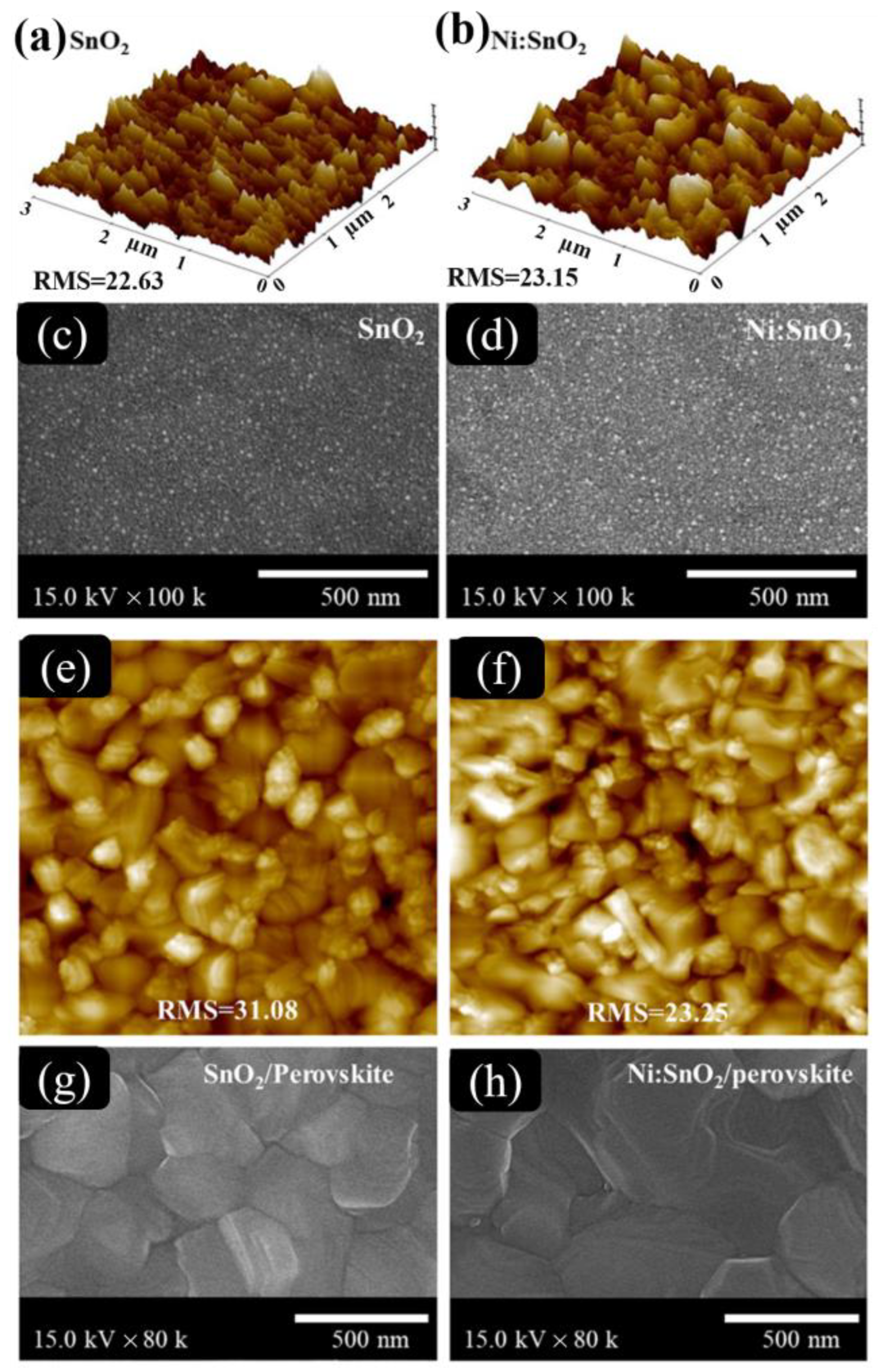
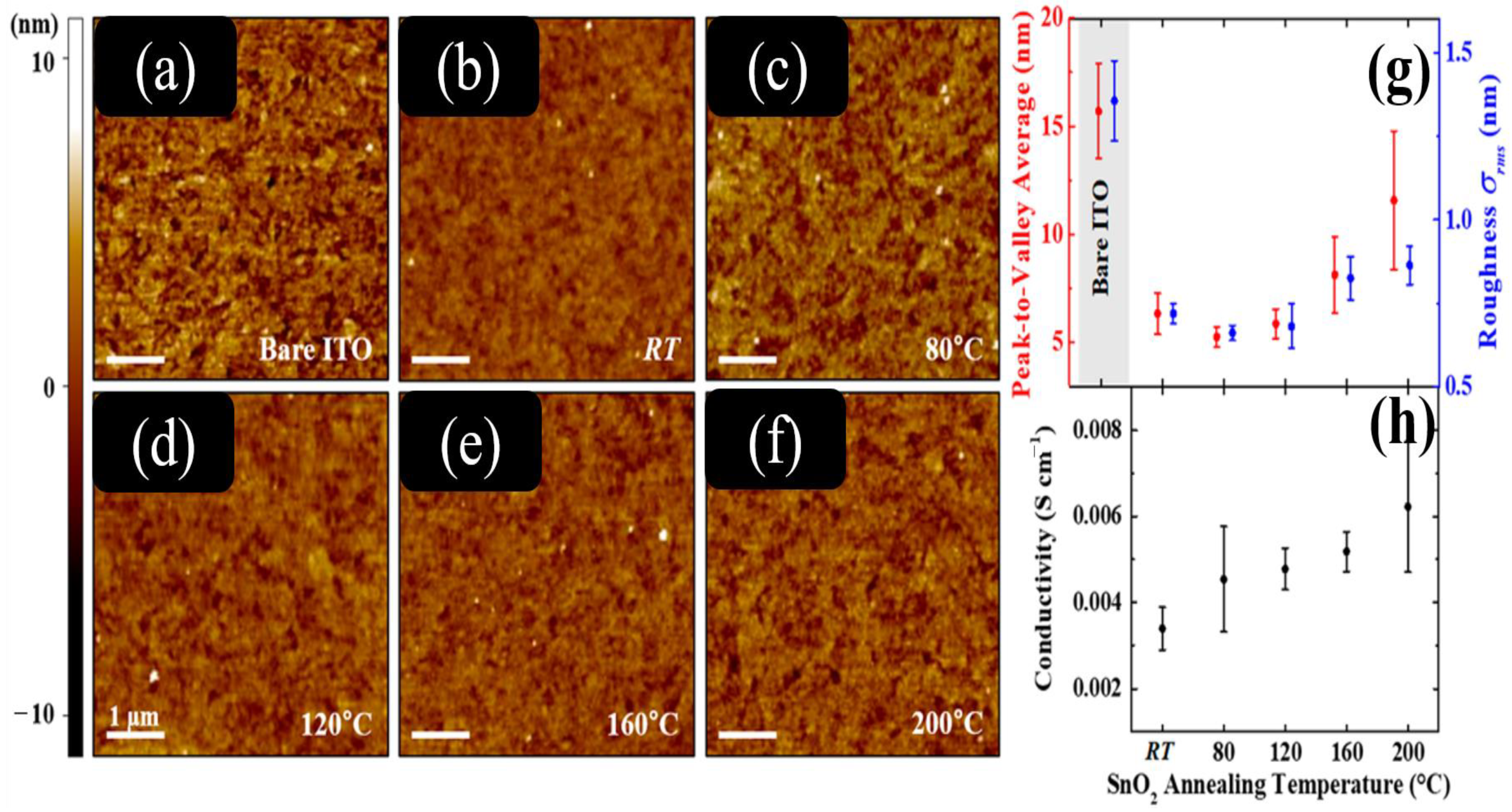
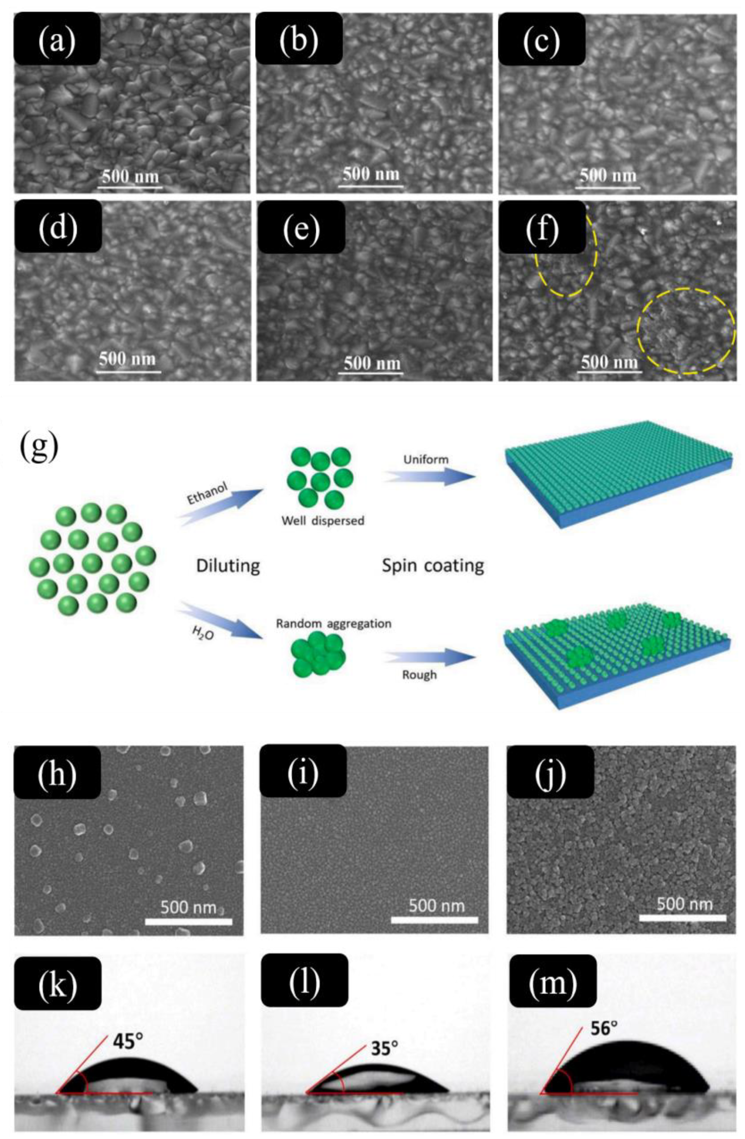
Eliminating the pinholes and reducing the roughness of the SnO2 surface have attracted considerable attention in academia. Determining the potential influence of these obstacles on the SnO2 surface is an important factor in achieving high-efficiency SnO2 utilization rates. However, there are diverse SnO2 surface effects. In addition, the thickness also seriously affects the surface properties of SnO2. The following is a detailed summary of the three factors that influence the potential for efficiently utilizing the SnO2 ETL, highlighting that interface engineering is a necessary strategy.

3.1. Pinholes

The perovskite active layer and SnO2 ETL in PSC devices are frequently disposed of using low-temperature synthesis methods. Because of the greater carrier mobility and reduced internal recombination of organic–inorganic hybrid perovskite materials, surface recombination is a key factor in determining the performance of PSCs. Recombination in SnO2 ETLs is primarily caused by inherent and bulk defects. Similar to other semiconductor supplies, the electrical and optical features of SnO2 are affected by point defects. Owing to their low binding energies, tin interstitials and oxygen vacancies are the two most widespread intrinsic defects on the SnO2 surface [55]. The majority of bulk defects are pinholes that are caused by the cracks in the SnO2 surface, which generate current leakage and lower the performance of PSCs. The performance of PSCs must be improved by lowering the power loss due to current leakage and delaying the charge recombination at the surface. Consequently, the pinholes is an un-intrinsic defect that mostly results from the surface deformation of SnO2 ETLs.
Although a decrease in performance is typically anticipated owing to inadequate surface coverage or pinholes, the effects of pinholes on performance metrics have been inconsistent. Surprisingly, the surface coverage has a greater influence on Voc than the pinhole size distribution. Nonetheless, the amount of surface coverage and the size distribution of the pinholes have an impact on the Jsc of the devices [68]. In addition, charge recombination at the HTL–ETL interface (caused by the lack of perovskite between them) can result in intriguing effects, such as impeccable device performance with inadequate surface coverage (Figure 3a,b) [69]. For various surface coverages, Figure 3c shows the photon volumetric integration absorbed per wavelength vs. perovskite (the diameter of the cell was approximately 1 µm). The results for the device with 100% surface coverage were used to normalize the obtained values. Here, the surface area affects the number of photons that the perovskite can absorb. Additionally, in the moderate-to-wide wavelength region (greater than 460 nm), this rise is nonlinear with surface coverage. The effect of light diffraction on gaps that are comparable to the light wavelength in dimension is discussed, where the relevant wavelength is in the 300–800 nm range and considerable diffraction occurs for gaps smaller than 300 nm (as shown in Figure 3d). Additionally, the gap functions as a circular light source if its size is smaller than the incident light wavelength [69]. Although the absorption rate varies nonlinearly with surface coverage for devices with small diameters (cell size of approximately 0.1 µm), the voids are minor in size for devices with large diameters (cell size of approximately 10 µm). Therefore, the photon absorption in the perovskite film varies linearly with surface coverage owing to the negligible light diffraction. Because of the higher recombination in the cell caused by the HTL–ETL interface, a subsequent drop in Voc is anticipated in devices with pinholes. Despite the reliance of Voc on the surface coverage, it has a relatively minor impact on the size of the voids. Therefore, owing to the different effects pinholes can have on the device performance of PSCs, it is necessary to transform the SnO2 ETL surface.

3.2. Surface Roughness
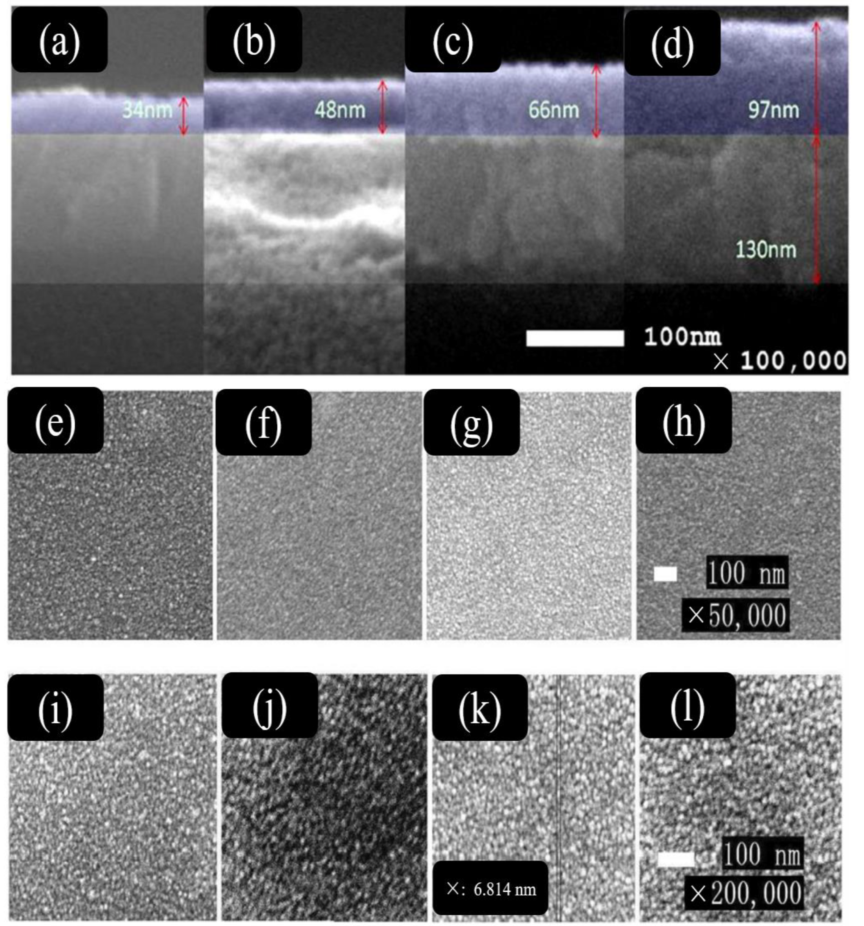
“Roughness” is a term that refers to the surface morphology of a material. Atomic force microscopy (AFM) and scanning electron microscopy (SEM) were used to assess the surface morphology of the coated films, where a smooth and dense surface is attributed to a good substrate with a low root-mean-square (RMS) roughness value. Currently, the SnO2 ETL surface and the perovskite surface coated on the SnO2 ETL are characterized as rough surfaces; however, the AFM of perovskite is beyond the scope of this review.
Typically, the SnO2 ETL modification procedure results in a decrease in the material surface roughness, resulting in a smooth and dense surface. According to Huan et al., the application of 2,2,2-Trifluoroethanol (T-SnO2) improves the smoothness of the SnO2 film surface [70]. This improvement was demonstrated via AFM analysis, which indicated that the roughness of the T-SnO2 ETL was 1.67 nm while that of the pure SnO2 ETL was 1.13 nm. However, there remain a few exceptions. With or without Ni+ doping, compact SnO2 films were spin-coated onto fluorine-doped tin oxide (FTO) substrates using a SnO2 colloidal dispersion solution [71]. Subsequently, both ETL films showed a flat surface, but the Ni:SnO2 film exhibited a rougher surface (23.15 nm vs. 22.63 nm) (Figure 4a,b); this is consistent with the surface morphology shown in the SEM image (Figure 4c,d). The Ni:SnO2 aggregates produced large particles when the mass concentration of Ni+ was greater than 1 mg mL−1, making it impossible to form an ETL layer that is smooth and dense. In other words, increasing the particle size changed the morphology of the SnO2 film, making the film thicker and rougher. Therefore, adjusting the concentration along with a suitable SnO2 particle size was essential to achieving effective PSC performance. Unexpectedly, the AFM on SnO2 and Ni:SnO2 perovskite films attained roughness values of 31.8 and 23.25 nm, respectively (Figure 4e,f), indicating that the SnO2-modified perovskite was smoother, as shown in Figure 4g,h. In addition, a 20 mm thick SnO2 film was prepared using spin coating and spraying on the FTO substrate, respectively, to evaluate the variations in surface morphology with the two approaches [72]. The film fabricated by applying spin coating yielded an RMS roughness of 14.1 nm and maximum variation of 92.2 nm, whereas that produced by employing spraying yielded an RMS roughness of 5.79 nm and maximum variation of 41.2 nm. Thus, the ultrasonic spraying technique exhibited significant development potential for flexible perovskite cells because it is well-suited for creating a SnO2 ETL on a large-area substrate. In general, modifying the surface of the SnO2 ETL results in a more uniform and smoother morphology than that of pristine SnO2 through AFM reduction, including synthetic and impurity incorporation, leading to a decrease in interfacial charge recombination. The smooth surface contributes to reducing the formation of large clusters on the surface and reducing pinholes, whereas rough surfaces are responsible for reducing surface wettability, not achieving coverage over the entire surface, and lowering device performance. In addition, the smooth surface of SnO2 contributes to improving electron mobility, enhancing electron transport in the SnO2 film [73,74].

3.3. Thickness

The morphology of the various interfaces in the PSC determines the ways in which the charge carriers are transported; thus, the morphology of the ETL–perovskite contact can be altered to promote electron transport and achieve the required performance. With an ETL thickness of more than 100 nm, the PSC may be hampered by the longer distance that the electrons need to travel to reach the top electrode and an increase in the recombination rate, which reduces the efficiency and fill factor of the cell [75]. Owing to its high transmittance, minimal leakage current at the ETL–perovskite interface, and low recombination rate, the film exhibited superior light transmission efficiency compared to an ETL thickness of approximately 30 nm [76]. However, thin films pose a technological challenge because of their extreme unevenness, which gradually increases the number of undesired interfacial defects [77]. Consequently, a 40 nm-thick film was determined to be excellent for obtaining a high fill factor because this size was enough to achieve high FTO substrate optical transmittance properties while still ensuring the prevention of pinhole formations and efficient carrier recombination [57,78].
The blocking of holes in perovskite layers, in addition to selective electron extraction, is another crucial role of the compact layers. The compact films should be consistent over the entire coverage of the FTO substrates to achieve an effective blocking effect. This prevents the top layers from coming into direct contact with the FTO substrates and reduces the shunt resistance of the channel. In this scenario, ensuring the blocking effect can be achieved by increasing the thickness of the compact layers [79]. However, thin compact layers are necessary to increase electron extraction and decrease charge recombination. Causing the intermediate phase to aggregate and develop rapidly during the manufacturing of SnO2 is not advisable because this would result in forming large-sized nanoparticles [80,81,82,83]. Thus, to create effective devices, well-dispersed single-crystalline particles must be prepared, and the phase of the crystalline particles and surface morphology should be regulated.
The content of SnO2 affects the layer thickness [84]. To produce a high-performance PSC, the SnO2 thickness should be approximately 64 nm with a concentration of 20%, whereas the perovskite thickness should be approximately 383 nm. This demonstrates that as the concentration of SnO2 increases, the Jsc of the device initially increases and then decreases. The Jsc of the 10% cell was the lowest, whereas that of the 20% cell was the highest. The most likely explanation is that when the SnO2 content changes, the film thickness increases, thereby increasing the resistance. Additionally, the film thickness affects the light transmittance. The ideal thickness to achieve high transmittance was from 40 nm to 60 nm [57]. Increasing the SnO2 film thickness will increase the light scattering caused by the formation of rough surfaces, significantly reducing the optical transparency. With an increase in the SnO2 concentration, the device Voc value rises. The likelihood of the holes moving to the FTO substrate, which is simple for charge carriers, decreases along the thickness of the SnO2 coating. Reducing the charge recombination at the interface is beneficial. The relative thicknesses of the films at various SnO2 concentrations were 33 nm (10%), 47 nm (15%), 65 nm (20%), and 98 nm (30%) (as shown in Figure 5a–d). Furthermore, the films exhibit poor continuity when the SnO2 concentration is 10%, and several groups of islands form, as illustrated in Figure 5e. These surface flaws add to the resistance value. When the content is increased to 20%, as shown in Figure 5f,g,i,k, the electrical conductance increases and the films remain clearly uniform. When the concentration reaches 30%, the reunion scenario manifests, which increases the resistance (Figure 5h,l). Additionally, the thickness of the changed layer affected how well the active materials used light by affecting the light transmittance of the film. The progressive increase in thickness was caused by an increase in the SnO2 concentration. Furthermore, the concentration, crystallinity, and electrical properties of the SnO2 film were expected to vary with the thickness of the film [85]. The high crystallinity of SnO2 enabled efficient charge transport and extraction from perovskite, improving device performance. However, it required SnO2 to be processed via a high-temperature annealing process, which easily caused the decomposition of SnO2 and limited its widespread applications in wearable electronic devices [86,87]. Currently, the low-temperature processing of SnO2 ETL has accomplished many achievements by retaining material properties comparable to those of high-temperature annealed SnO2, contributing to further improvement of PSC performance [88]. However, more research is required to determine the impact of the SnO2 thickness after 250 °C annealing. Because the thickness can be adjusted by changing the concentration during the spin coating process, the content of the precursor solution was varied. In terms of PV performance and hysteresis, the precursor concentration and annealing temperature were crucial. An approximately 40 nm-thick SnO2 film with an amorphous nature was discovered to be ideal for obtaining excellent performance with minimal hysteresis because the film morphology contributed to enhancing electron transport and reducing the defects formed in the perovskite crystal structure, which lowered the carrier recombination [70].

4. Interface Design Rules for Efficient SnO2 ETL

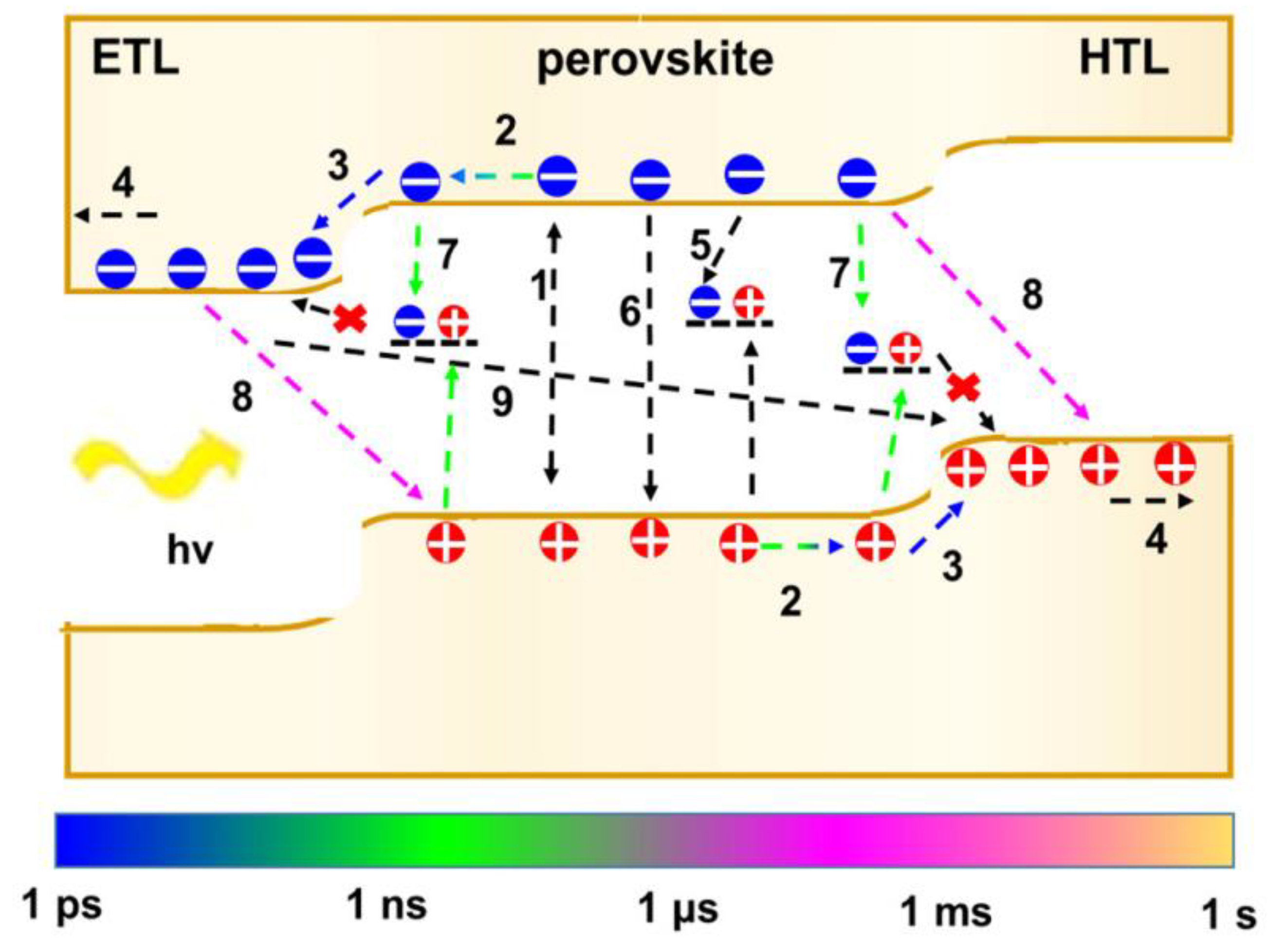
4.1. Charge Carrier Transport

A detailed diagram of the PSC charge dynamics is shown in Figure 6. Sunlight exposes the devices to photons, which the perovskite absorbs and converts into excitons. Owing to the low exciton binding energy, the excitons split into holes and electrons at ambient temperature. The charge-carrier lifetime had a duration of 10–100 ns [89]. Both the holes and electrons were moved to the perovskite–HTL and perovskite–ETL interfaces under the effect of the electric fields and carrier concentration gradients, respectively. The interface area experiences a continuous potential drop caused by the offsets in the valence and conduction bands, which ensures that charge transport is moved back to the HTL or ETL before their annihilation, typically within a timeframe of 100 ps [89]. Finally, the corresponding electrodes gather the electrons and holes. The internal quantum efficiency (IQE) should be extremely close to 100% if each absorbed photon produces a different hole–electron pair and all charge transport is gathered by the electrodes [90,91]. As a result of the carrier recombination occurring in the bulk perovskite or at its grain boundaries, at the interface of perovskite–HTL, or perovskite–ETL and HTL–ETL interfaces when perovskite is missing in some places, the usual IQE of PSCs is approximately 90% [92,93].
The mechanism behind charge-carrier transport in planar PSCs is typically clarified by measuring the transient photovoltage (TPV) and transient photocurrent (TPC) [31,95,96]. A bi-exponential function was used to fit the photovoltage (Vph) decay traces. Accordingly, the following equation was used to determine the apparent recombination time constant (τr) and transport time constant (τt):
τ = A 1 τ 1 + A 2 τ 2 A 1 + A 2   ,
where A2 and A1 are constants that define the impact on decay with lifetimes τ1 and τ2, respectively. With an increase in Vph, the τr value shifted from milliseconds to microseconds. Notably, the connection between τr and Vph for planar PSCs on the semi-logarithmic axis exhibits a roughly linear correlation, suggesting that the charge-carrier recombination process should proceed in a manner similar to that of trap-limited recombination [97].
To determine the amount of charge (q) in a cell, current transients were unified with respect to time. The following equation was used to determine the overall charge density (n) [98]:
n ( V p h ) = q ( V p h ) / e d A
where d is the thickness of the photoactive layer in the device, e is the elementary charge, and A is the device area. Thus, the important elements in regulating the accumulation of carriers and minimizing the recombination of defects, for instance, ETL layers and their interaction with the perovskite film, should be considered to increase the effectiveness of the devices used under such settings. Creating a smooth surface and thin layer of SnO2 has been proven as an efficient method to increase the quality of an SnO2 ETL, contributing to minimizing the formation of defects on the surface of the perovskite layer and improving PSC performance [99,100].

4.2. Non-Radiative Recombination

Surface flaws, reverse charge carrier transfer, and mismatched energy levels are the main causes of interface-induced non-radiative recombination. Effective interfaces should block minority carriers and extract only the dominant carriers. Because perovskite and ETLs exhibit distinct bandgaps, a power cliff or spike (EC) must occur at the interfaces, such as that at the ETL–perovskite contact. The ETL carriers could readily go over the barrier to return to the surface in a scenario where there was a surface with a structural cliff. The forward bias condition would result in the annihilation of electrons and holes because of the many defects functioning as recombination foci for charge transport at the ETL–perovskite interface (Figure 7a). An increase in the barrier (EC) against the ETL electron reverse insertion into the interface with a forward bias can result from the spike in the conduction band (CB) at the interface (Figure 7b).
The charge injection–accumulation–diffusion-model-based nanocrystal charge transfer dynamics are shown in Figure 7c, together with the recombination and charge transfer related to SnO2 nanoparticles (Figure 7d). Conventional nanoparticles typically have several organic molecules bonded to their interfaces, which causes deep-level flaws. These conventional nanoparticles are formed from the precursors of metal oxides disseminated in an organic solvent [101]. Additionally, owing to the low construction energy, the inherent deep-level flaws in ETLs include transition metal defects (Ti3+ or Ti4+), oxygen vacancies with positive charges (VO+, VO++), and intrinsic defects (Sni) [102]. These flaws may trap charge transfers and lead to charge recombination.
In addition, a vital factor in preventing charge accumulation is the balanced transit of holes and electrons throughout the entire cell. Owing to the existence of shallow-level defects in ETLs, including vacancies of oxygen with no positive carriers called VO0, electrons transferred from the perovskite layer to ETL layers may be trapped before being released and returned to the CB upon thermal excitation. Nanoparticle metal oxides were used to create a crosslinked ETL network. The crystalline components were joined together or in amorphous equivalents. The carrier transfers in the ETL layers, particularly in TiO2 and SnO2, have been extensively explained by the fluctuation-induced tunneling conductivity (FITC) mechanism. The effective tunneling width, w, effective tunneling area, A, and zero-field barrier height, B, play significant roles in the carrier transit rate through the junction.
This is a direct outcome of the Shockley–Queisser equation regarding the carrier recombination current density [103]:
J r a d = J 0 , r a d × e Q F L S / k T ,
where J0,rad is the generated current density, QFLS is the quasi-Fermi level splitting, T is the absolute temperature (26 °C, i.e., kT = 25.8 meV), and k is the Boltzmann constant. In addition, the QFLS is calculated based on the free energy of the electron and hole pairs produced in the film when illuminated by an equivalent of 1 sun [104].
Q F L S = k T l n   ( P L Q L × J G J 0 , r a d ) ,
where PLQL is the photoluminescence (PL) quantum yield and JG denotes the generated current densities under illumination.

4.3. Surface Trap

The defect density within the ETL–perovskite interface has a significant impact on PSC performance. The optoelectronic properties are destroyed by electron or hole entrapment and recombination caused by the defect levels inside the bandgap [105,106,107,108]. The perovskite absorber surface and grain boundaries are located where deep-level flaws are most frequently present [109,110,111]. Thus, interface engineering is crucial for preventing non-radiative procedures that convert electricity into thermal power by transforming “active” interface flaws into “inert” defects. The high density of defect states in a SnO2 film presents another difficult problem. It has been suggested that the SnO2 surface contains a significant number of Sn dangling bonds, which can absorb O2 and H2O from the atmosphere, trap electrons in the conduction band for recombination, and create potential barriers to block electron transition [112]. Many Sn dangling bonds are present in the SnO2 ETL layer.
Sn atoms saturate the surface Sn dangling bonds after (NH4)2S is added to SnO2 colloids, forming S-Sn bonds [113]. As a result, surface oxygen vacancies may be eliminated by the creation of S-Sn bonds. Additionally, as shown in Figure 8a–c, the interface Sn-S bonds can prevent moisture from penetrating the cell. Moreover, the interfacial S-Sn bonds create a bond with the Pb atoms for S-Sn-Pb formation in the perovskite crystalline procedure. The efficiency of electron extraction is increased by the direct connection of perovskite to the electron transport channel. By lowering the defect density on the ETL’s surface, this method lowers the barriers to electron transport and boosts electron mobility, conductivity, and stability. In addition, the interfacial trap defects can be effectively reduced through the creation of I-Sn bonds at the surface, and Cl diffusion in the perovskite layer positively affects the film crystallinity [114].
Although the high-frequency capacitances presented in Figure 8d are nearly undetectable at frequencies above 100 Hz, the low-frequency capacitances clearly differ depending on the annealing process of SnO2. As the preparation processes for the examined devices, with the exception of the SnO2 annealing temperature, were the same, the variations in the low-frequency capacitances were solely due to the contributions of the ETL–perovskite interfaces instead of other components, such as HTLs and perovskite layers. Through repetitive charging and discharging, the cell capacitance increases in response to low-frequency perturbations caused by the deep-level traps at the interfaces [115,116,117]. The defect density state, Ew vs. nt (=E − Ebandedge), was calculated from the capacitance–frequency diagram [118]. The deep-trap distribution noticeably changes when nt values under various temperatures are examined, as shown in Figure 8e, demonstrating that the SnO2-annealing temperature affects the defect generation at the ETL–perovskite interface.
Figure 8. Modification of the interface mechanism. (a) H2O and O2 enter the SnO2 surface, (b) S-O and S-Sn bonds form to stop H2O and O2 from entering, and (c) Sn-S-Pb anchors form to lessen the interfacial trap states. Reprinted with permission from Ai et al. [113] Copyrights 2019 by International Solar Energy Society. Published by Elsevier Ltd. The electronic trap states and effects of annealing temperature of the solar cells with (d) capacitance–frequency plot and (e) trap distribution spectra. Reprinted with permission from Yun et al. [119] Copyrights 2019, American Chemical Society.
Applsci 13 10715 g008
The following equation can be used to compute the trap density (ntrap) [120,121]:
N d e f e c t = 2 ε 0 ε r V T F L e L 2   ,
where L is the thickness of the perovskite films, e (1.6 × 10⁻¹⁹ C) is the element charge, ε0 (8.85 × 10⁻¹⁴ F cm−1) is the vacuum permittivity, εr is the relative dielectric constant, and VTFL is the trap-filled limit.
The effective defect density as a function of f is described as follows [122,123]:
n 0 ( f ) = N 0 1 + ( 2 π f ) 2 τ d a m 2 ,
where τdam is the time constant for carrier emission and capture and N0 = n0 (f = 0). For various damaged materials, we can use this equation to calculate the effective defect density, n0(f), and trap time constant. τdam.

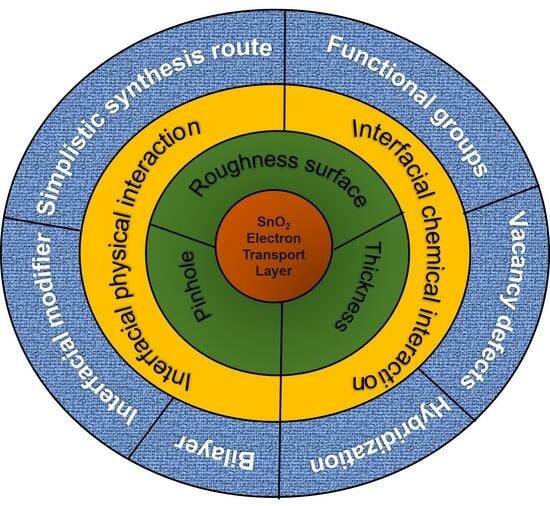
5. Surface Engineering of SnO2 ETL

Surface engineering is an effective method to enhance the PSC’s performance through the smooth and dense surface formation of the SnO2 ETL. There are diverse approaches for fabricating SnO2 ETL surface supports. Some methods interact by associating impurities and physically acting on a surface. In addition, many studies have altered the surface through straightforward possessions on the O-Sn-O bond. Thus, we have classified surface engineering into the two following categories: (1) interfacial physical interaction (including surface modification processes caused by the synthesis route, modifier, and bilayer); (2) interfacial chemical interaction (including surfacing caused by functional groups, hybridization, and vacancy defects).

5.1. Interfacial Physical Interaction

Physical interactions were determined when the approach did not affect the O-Sn-O bond but only affected the crystal structure, morphology, and surface features of the ETL.

5.1.1. Simplistic Synthesis Route

The surface of the SnO2 ETL can be modified using diverse SnO2 facile manufacturing techniques, generating high-efficiency PSCs. This amalgamated comprehension indicates that the SnO2 ETL is typically fabricated at low temperatures. Nevertheless, such synthesis routes are impotent, providing the generated SnO2 film with a sufficient annealing treatment to eliminate additives and encourage strong interactions between the nanoparticles. As a result, PSCs with a SnO2 layer as an ETL were utilized to contemplate the dependence of the cell performance on the SnO2 annealing temperature [119]. The nanoscale optical/electronic and morphological characteristics of an SnO2 ETL were investigated at various annealing temperatures (room temperature to 200 °C) to understand the influence of annealing on the SnO2 features and confirm the components influencing the PSC performance. Understanding the effect of the annealing temperature on the layer features and ETL performance is crucial for realizing an effective PSC using a low-temperature technique, which broadens the scope of its commercial applications. The morphology of the SnO2 ETL surface was investigated to understand how variations in its surface homogeneity modify the solar cell performance, which was impacted by the annealing conditions based on ITO topographies; accordingly, diverse SnO2 films are depicted in Figure 9a–f. Generally, the deposited SnO2 layers attain a noticeably smoother surface. Compared to the bare ITO, the SnO2 ETL surface was smoother at different temperatures. Regardless of the annealing temperature, layers were successfully produced at different temperatures in 30 min. Additionally, the surface roughness was quantified using the RMS and peak-to-valley average values (Figure 9g), demonstrating that the SnO2 ETL film attains a uniform and smooth surface when it is annealed at temperatures below 155 °C. The average RMS values of SnO2 at 200 °C and 160 °C were higher than 0.8 nm, whereas those of SnO2 treated at low temperatures were 20% smaller. At 160 and 200 °C, the peak-to-valley roughness also increased dramatically. The rate of solvent evaporation is thought to fulfill the role according to the shape of the SnO2 nanoparticle layer, which changes with respect to annealing temperature. As the thickness of the deposited SnO2 layer is discovered to be 20 nm, the detected roughness values of SnO2 at 160 and 200 °C are significant and degrade the contact with the perovskite top layer by forming shunting channels similar to pinholes. It is well known that the nanoscopic morphology of the ETL and formation of shunting paths have a significant impact on the charge collection efficiency and shunt resistance of solar cells; thus, it is anticipated that the uniformity of the SnO2 ETL will have an effect on both the JSC and FF of the PSC [124,125,126,127]. As a result, the lower JSC and FF of the high-temperature processed SnO2 are attributed to the rough surface. Although the electrical conductivity increases with higher annealing temperatures (Figure 9h), it does not seem to be a factor that affects the charge transfer within the relatively thin ETL (20 nm). An SnO2-nanoparticle-based uniform layer was systematically examined. The highest efficiency of 19.0% was obtained by annealing at 120 °C while adjusting the temperature from ambient temperature up to 200 °C. The low-temperature processing of an SnO2 ETL results in a smooth and uniform SnO2 surface, reduced trap density, optimal band alignment, and shifting toward the bandage, all of which contribute to creating efficient PSCs.
Because of the generation of SnO2 at low temperatures and the simplicity of the manufacturing process, a solution-based technique was used. In addition, the constructed SnO2 ETLs function effectively without heat annealing. However, SnO2 generated by magnetron sputtering is infrequently documented, despite the great dependability, maturity, and competence of the sputtering process in both industry and laboratories [128]. Additionally, on a 10 nm SnO2-coated FTO, tiny perovskite grains tended to crystallize at the SnO2–perovskite interface, which negatively impacts the carrier transport efficiency. The volumetric expansion and ion migration that occur during the crystallization of perovskite are hampered by a rougher surface because, owing to the roughness, the materials are slowly coated onto the substrate at rates of only a few angstroms per second. However, when perovskites are created using solution methods, this issue is less significant because the ion precursors can easily travel over the substrates without having to overcome significant energy obstacles. Consequently, this issue has not been frequently explored in depth. Nevertheless, even though perovskite produced on solution-processed SnO2 films attained a grain size comparable to that of perovskite developed on sputtered SnO2 films, most of the grains in the former perovskite films had layered structures. This might be explained by the SnO2 film undergoing solution processing being rougher, which yields a variable perovskite crystallization rate and degree, as well as a considerably rough surface. This may enhance the likelihood of charge recombination at the ETL–perovskite interface. As a result, compared to the sputtered SnO2 film on FTO glass, which demonstrated good transparency with a transmittance close to 90% in the visible range, the solution-processed SnO2 exhibited a lower transmittance of approximately 80% (Figure 10a). Additionally, the UV–vis absorption spectra of the vapor-deposited perovskite presented in Figure 10b demonstrate good absorption in the visible band. Additionally, the spectra demonstrated that sputtered SnO2 attained better absorption than solution-processed SnO2 for perovskite, which was explained by the latter’s lower transmittance compared to that of sputtered SnO2. When the perovskite film was deposited over sputtered SnO2 as opposed to solution-processed SnO2, the perovskite PL peaked at 788 nm, and the steady PL displayed a more pronounced quenching, which is consistent with the estimated values (Figure 10c). Room-temperature-sputtered SnO2 showed an even higher transmittance compared with other high-temperature-generated spin-coated SnO2 films. Using a straightforward sol–gel technique, Shi et al. created homogeneous SnO2 NPs at ambient temperatures. The remaining Cl on the surface caused the perovskite to partially decompose [129]. The hydrous SnCl4 was dissolved to 0.05 M and then hydrolyzed at ambient temperature. To gather the SnO2 NPs, butyl acetate was used as a precipitator. UV–ozone (UVO) treatment was used to remove the Cl residue after spin coating the substrate to lessen the hysteresis. These ETLs did not require additional heat processing. The highest PCE for a flexible and rigid PSC were 15.27/14.74% and 19.22/18.79% (RS/FS), respectively.
The UVO treatment of the SnO2 ETLs altered the performance of the planar PSCs at various time intervals [130]. A 30 min treatment period was found to be ideal. The characterization results revealed that the SnO2 film became more hydrophilic with a contact angle of 24.5° by extending the UVO exposure period (30 min), which supported the elimination of organic residues associated with the precursor reagents at the film surface (as shown in Figure 10d–g). It is possible to use UVO treatment to improve the perovskite layer coverage and ETL–perovskite interface, which facilitates the electron transfer from the perovskite film to the ETL. Interestingly, the cells based on SnO2 did not significantly decrease the efficiency of solar cells when exposed to UVO for more than 30 min. Furthermore, as seen in Figure 10h,i, the continuity of the SnO2 films treated with UVO for 0 and 10 min was subpar, with evident voids and non-uniform coverage. The ETL and HTL layer separation were caused by the non-uniformity break, creating recombination centers and impairing the PSC performance. It was discovered that thin films without pinholes and cracks were formed as the UVO treatment period increased (Figure 10j,k). The ETL–perovskite interface was improved by increasing the wettability of the SnO2 layer, which also decreased recombination and increased electron injection. This was explained by the fact that the oxygen atoms chemisorbed during UVO treatment contributed to the formation of hydroxyl groups on the SnO2 surface. Therefore, the oxygen vacancies were reduced, film wettability was enhanced, and the ETL–SnO2 interface was improved [131,132]. The effects of UVO treatment include the following: (1) increasing the wettability of the perovskite film and (2) passivating the ETL surface by lowering the recombination centers and increasing Jsc. Contemporary approaches to altering the surface morphology are also highlighted. The increasing need for additive patterning of functional multilayers and device components can be achieved using inkjet technology [133]. The process is easily scalable to the meter format and delivers direct, cost-effective, and mask-free patterning. Compared with the commonly used spin coating process, the inkjet printing approach has attracted considerable attention regarding the up-scaling manufacturing of PSCs, together with lower material consumption and negligible waste. In this study, the inkjet printing techniques for TiO2, SrTiO3, and SnO2 ETLs were assessed. The drying qualities of the cosolvent are advantageous for uniformly producing SnO2 films by optimizing the PSC performance based on the printed ETLs. The low-cost printability of the method, particularly beneficial for flexible PSCs, is one of its encouraging features. However, it is currently difficult to print a vast and uniform ETL on rough and brittle plastic substrates without hysteresis. High-quality SnO2 films for flexible PSCs with high efficiency can be created using a slot-die method. Regardless of the fabrication technique, the intrinsic hysteresis caused by the SnO2 layer is controlled using the potassium interfacial passivation strategy [134]. K + cations facilitate the formation of perovskite grains, passivation of the interface, and increased stability and efficiency. The large (5 × 6 cm2) flexible modules reached an efficiency greater than 15%, while the small flexible PSCs had a high efficiency of 17.18%. This passivation approach shows great promise for improving the performance of flexible PSCs covering wide areas.

5.1.2. Interface Modifier
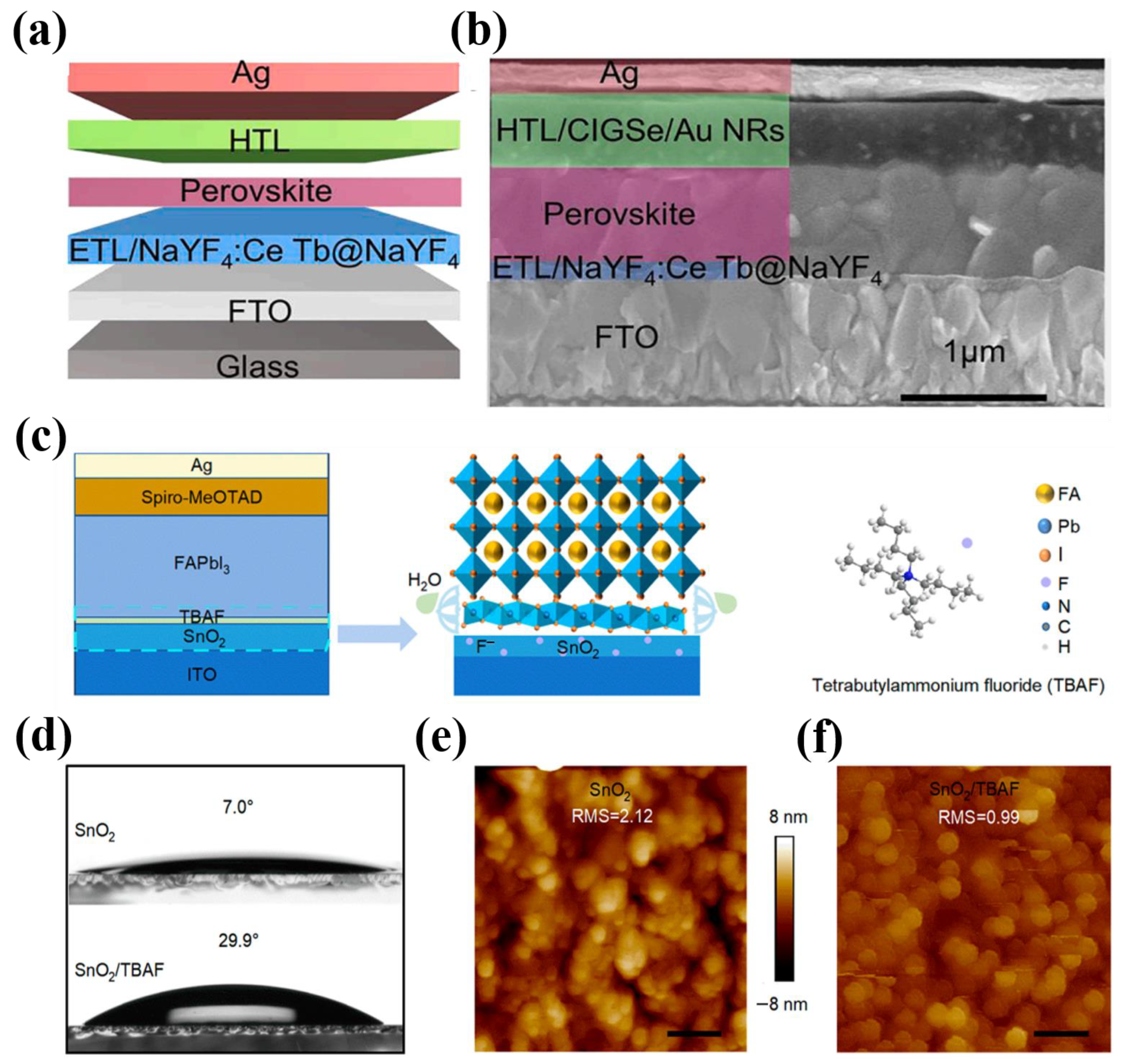
The unique aspect of this study is that, unlike previous studies that attempted to passivate SnO2 with chlorine, NH4Cl is used here without a doping procedure and placed on the SnO2 layer as a modifier [135]. Furthermore, the precursor for SnO2 is an inexpensive salt of SnCl4·5H2O. In general, the doping-free surface treatment is concentrated. The surface roughness of SnO2 can be successfully reduced using NH4Cl as a modifier, leading to a smooth surface for the ETL. To produce PSCs based on the ETL, a smooth ETL surface is crucial because a rough ETL may produce numerous pinholes that act as electron–hole recombination sites between the ETL and the perovskite layer, increasing the series resistance (Rs) and deteriorating the PSC performance. Additionally, a smooth ETL surface can provide better physical contact with the perovskite layer, boosting shunt resistance (Rsh) and improving the performance of planar PSCs. Furthermore, NH4Cl surface treatment can increase the surface coverage and shunt resistance; however, as the concentration of NH4Cl increases with respect to that of SnO2-Cl3, the surface uniformity declines, which can increase the number of undesirable pinholes known as recombination centers. According to Figure 11a–f, the surface morphology of the unaltered and modified SnO2 exhibits uniform grains, complete FTO coverage, and a smooth, pinhole-free compact morphology. Naturally, NH4Cl-SnO2 films become less uniform at higher NH4Cl concentrations (0.02 M), as indicated by the yellow dotted circles in Figure 11f, which is due to the residual solution on the surface. When subsequent layers are deposited over these regions, pinholes may occur, reducing the performance of the PSC. The existence of Cl upon transformation is clearly visible, indicating that NH4Cl was successfully incorporated into SnO2 without a significant negative impact on the bulk structure of SnO2. By incorporating ethanol into the commercially available SnO2 precursor, the SnO2 ETL surface can be successfully regulated (Figure 11g) [136]. This method increased the stability and wettability of the SnO2 precursor on the glass substrate. Thus, using ethanol helped create a SnO2 film with a uniform morphology that was devoid of aggregation, which also improved the perovskite crystal quality. Compared to the other samples, dimethylformamide (DMF), a polar organic solvent, may have a long-lasting effect on the surfactants in the SnO2 colloid dispersion because the DMF-SnO2 film exhibits a clearly non-uniform film shape and large aggregations (Figure 11h–j). The properties of the ETL–perovskite interface are typically substantially affected by the shape of the SnO2 film, which in turn affects the internal resistance of the perovskite. To produce high-performance PSCs, the ethanol-SnO2 film surface must be flat. Additionally, the water contact angles of the various SnO2 film types show how the wettability of the dripping solution differs (as shown in Figure 11k–m).
It has been confirmed that treating SnO2 with alkali salts enhances the performance of PSCs, which is attributed to fewer surface defects [112]. As a result, the impact of various alkali fluorides has been researched [137]. The incorporation of SnO2 with KF, RbF, and CsF can accelerate charge in PSCs, reduce defect density, and improve the electrical properties of SnO2. The type of cation will determine the function of the alkali cation. Particularly, the smaller cations, such as the Rb+ and K+ cations, can migrate into the upper perovskite layer, which reduces defects and, consequently, limits recombination in the perovskite layer. This results in a much improved Voc of the corresponding device. The Cs+, on the other hand, prefers to stay on the SnO2 film to increase the electrical conductivity of the ETL and to improve the energy band alignment with the perovskite layer in the device, which primarily improves the fill factor of the device. However, due to their heterogeneity and undesirable aggregation, LiF and NaF are not suited for the post-treatment of SnO2 films. It might be because LiF has a weak crystallization characteristic in aqueous solutions, which causes microcrystallites to form on the film [138]. Therefore, the aggregation of free nuclei during the crystallization of NaF is most likely the cause of the uneven morphology of film [139].
Researchers have sought after suitable passivation materials that can align with the energy band and reduce the defect density. Halide substances, such as KCl and NH4Cl, are potential solutions to these issues. The mechanism of halide ions at the interface must be clarified, and the preparation procedure must be investigated [140]. The impacts of SnO2 surface halogenation on the performance of PSCs were thoroughly examined. Tetrabutylammonium chloride (TBAC), tetrabutylammonium bromide (TBAB), and tetrabutylammonium (TBAI) were used to passivate the SnO2 surface, and the concentration gradient of the passivation solution was investigated. The favorable effects of SnO2 surface halogenation on the SnO2–perovskite interface characteristics were clearly observed through the extensive characterization of perovskite layers and PSC devices. Charge carrier dynamics were examined to investigate the reasons behind the enhanced performance of interface-designed devices. Theoretical studies and experimental results demonstrated that TBAC might be the best passivation material for SnO2 surfaces. The concentration of the solution also increased the visibility of the passivation effect. TBAC might encourage the development of perovskite crystals, reduce interface flaws, and boost the internal recombination resistance. It was evident that the size of the perovskite particles increased after the addition of TBAC, and the defect density between the particles also decreased to some extent. This directly lowered the recombination center, encouraged charge transfer, lowered carrier recombination at the interface, and increased device stability. On the other hand, the addition of TBAB also resulted in a larger particle size, but there were still more holes, and TBAI had little effect on the growth of perovskite crystals. As a result, Cl was the best halogen anion for SnO2 surface passivation and might efficiently promote the development of a perovskite layer. Consequently, the PV performance of PSCs was enhanced. Halide ions may interact with Sn atoms on the SnO2 surface, increasing the charge density and enabling a high-efficiency charge extraction. This research highlights the importance of enhancing the PV performance of PSCs and offers practical guidelines for the interface engineering of PSCs to achieve high efficiency.

5.1.3. Bilayer

During the formation of the perovskite layer, oleic acid ligands can passivate the trap sites [141]. Controlling perovskite layer defects can be extremely important for perovskite grain boundaries and ETL–perovskite heterointerfaces, resulting in PSCs with improved solar performance. Enhancing the perovskite crystalline quality can reduce the internal defects of the active layer and current loss caused by the internal non-radiative recombination of the device (Figure 12a). As a result, the PV performance is synergistically improved via the NaYF4:Ce and Tb@NaYF4 nanocrystals acting as light scattering centers, UV down-converters, and defect passivators. A cross-sectional image of the PSCs captured using SEM is displayed in Figure 12b. SnO2 was coated on the FTO conductive glass with a thickness of 20 nm, and spin coating was used to manufacture NaYF4:Ce, Tb@NaYF4 nanocrystals on SnO2 (50 nm). The perovskite active layer, FA0.85MA0.15Pb(I0.85Br0.15)3 (400 nm), was created by using a one-step spin coating technique. Before being added to the HTL, spiro-OMeTAD was mixed with Cu-In0.7-Ga0.3-Se2 (CIGSe) quantum dots and Au nanorods (NRs) (205 nm). A silver electrode (117 nm) was placed on top of the device. The addition of NaYF4:Ce and Tb@NaYF4 phosphor nanocrystals improved the crystalline quality of the perovskite, reduced the recombination of grain boundaries, and boosted the utilization of UV light by light down-conversion. The natural deterioration of perovskites is a possible explanation for this phenomenon. The main reason for this phenomenon was the natural degradation of the perovskite. The NaYF4:Ce,Tb@NaYF4 affected the long-term stability of the perovskite layer because it enhanced the crystallinity of the perovskite films. The increased grain size of the perovskite films reduced the grain boundary density, which enhanced the resistance of the perovskite films to the water and oxygen in the environment. In addition, the main reason for the moderately enhanced device stability of NaYF4:Ce, Tb@NaYF4 nanocrystals was the presence of thinner oily ligands on their surfaces after the synthesis process. The hydrophobic nature of oily ligands enabled the perovskite film to improve its stability under humid conditions. The NaYF4:Ce, Tb@NaYF4 enhancement increased the crystallinity of the perovskite films, which was the key factor affecting their long-term stability. The larger grain size of perovskite films results in a decrease in the grain boundary density, which improves their resistance to oxygen and water in natural environments (Figure 12c) [142]. The increased hydrophobicity of the improved film helps to increase the interfacial contact, lessen the upper perovskite grain boundary defects, and prevent heterogeneous nucleation. The grain boundary movement was hampered because the wetting surface’s grain boundaries were tethered by imperfections on the ETL surface. As a result, the enhanced hydrophobia suggested that the flaws at the perovskite grain boundaries were being reduced, improving the perovskite active layer’s quality. This could be attributed to the ETL surface’s smoothness and lack of wetness, which inhibit heterogeneous nucleation and promote grain boundary migration. This finding demonstrated that perovskite could grow its grain sizes due to its hydrophobic surface. Less grain boundary defects were present in the larger grain sizes, which reduced charge non-radiative recombination at the perovskite–ETL interface. Figure 12d displays the contact angle measurement results. After the addition of tetrabutylammonium fluoride (TBAF), the contact angle increased from 7.0° to 29.9°. Furthermore, the RMS roughness of the SnO2/TBAF film (0.98 nm) was lower than that of the SnO2 film (2.12 nm) (Figure 12e,f); the former film was smoother and more homogeneous. Owing to the uneven surface, this may provide a superior substrate for the deposition of perovskites and successfully stop further recombination loss. The creation of 1D perovskite (TBAPbI3) favorably inhibits the decomposition of perovskite and the enhanced SnO2(TBAF)–perovskite interface, improving the stability of the modified film. The addition of TBAF to the SnO2–perovskite interface significantly increased the effectiveness and stability of the PSCs. Along with increasing the SnO2 conductivity, the TBAF interface modifier also passivates the perovskite flaws. Additionally, the decomposition of perovskite and phase transition can be efficiently inhibited by the 1D perovskite (TBAPbI3) generated by TBAF and PbI2 in perovskite, which help promote the stability of PSCs. The TBAF multifunctional interface modification resulted in PSCs with a high efficiency of 23.1%, resulting in outstanding thermal and humidity stability.

5.2. Interfacial Chemical Interaction

A chemical interaction refers to a direct interaction with O-Sn-O bonds, in which the formation of bonds between the agent and O and Sn sites is seen as a positive solution that alters the properties of the SnO2 ETL.

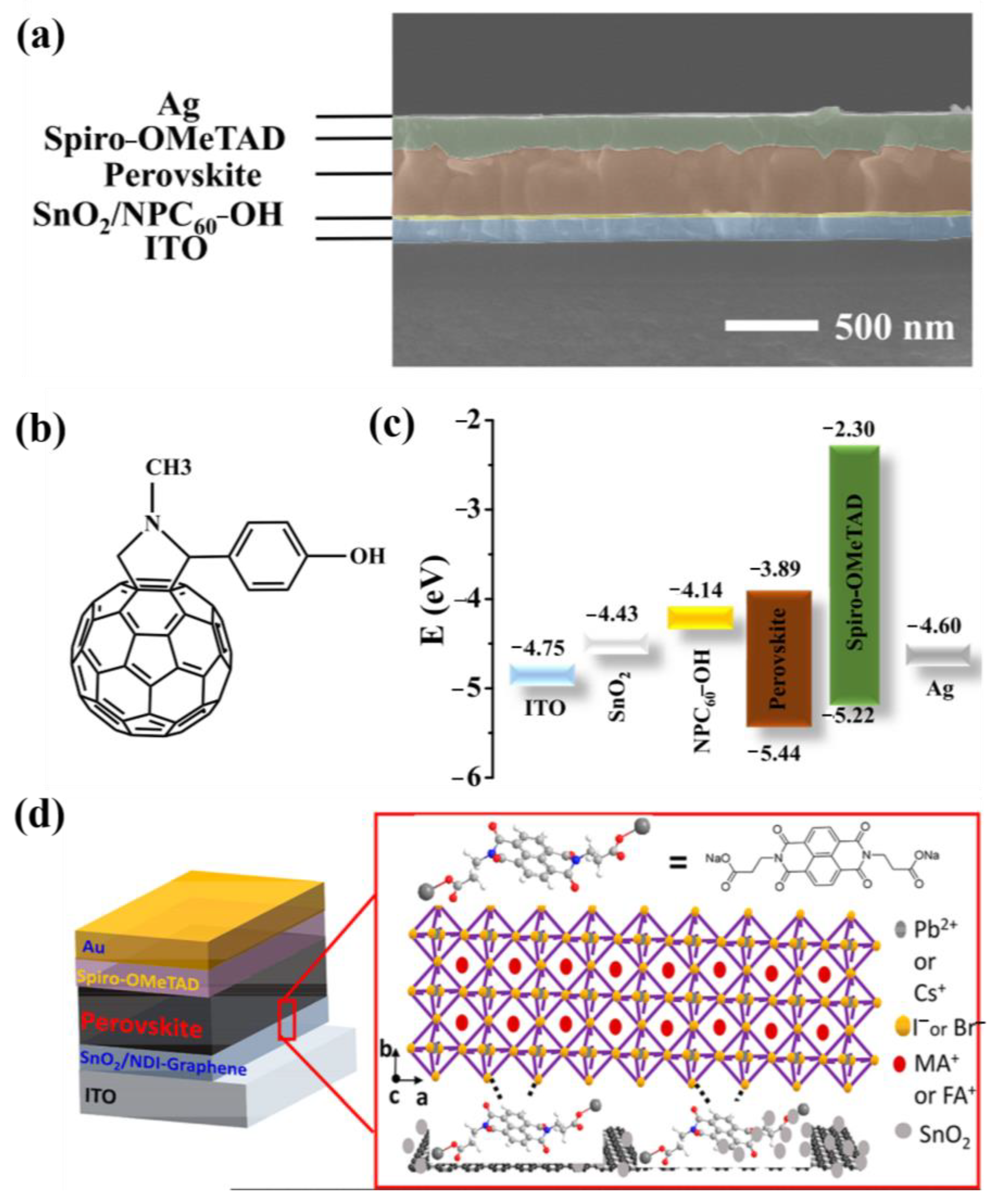
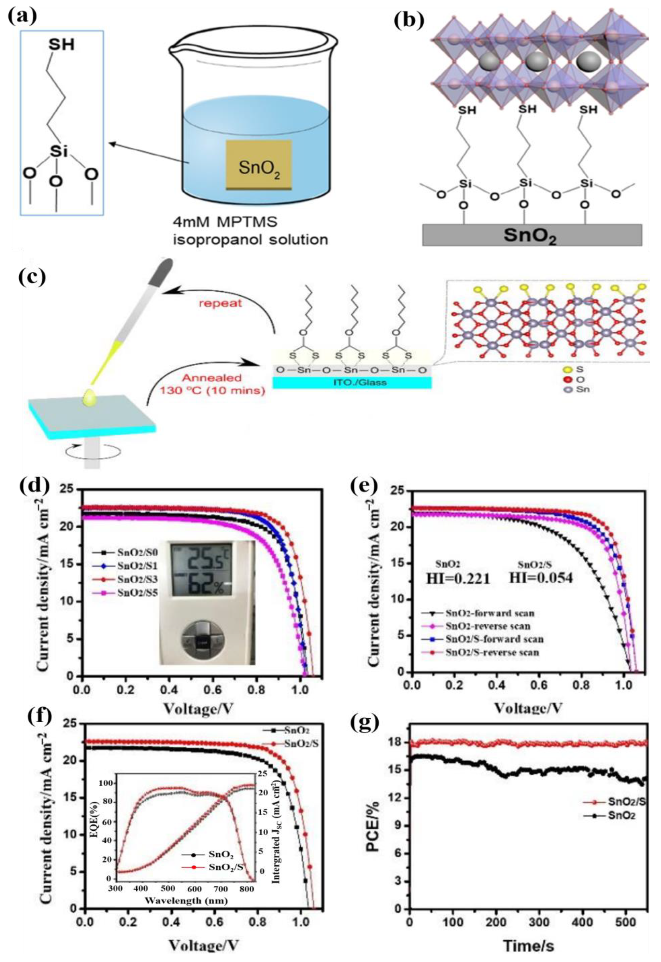
5.2.1. Functional Groups

ETL–perovskite interfacial passivation is a particularly challenging scientific topic because it involves using polar solvents (such as dimethyl sulfoxide (DMSO) and DMF) for perovskite solution deposition, which often destroy the bottom as-formed defect passivation layers [143]. Thus, it is highly desirable to develop a unique multifunctional ETL capable of both electron transport and the passivation of the bottom surface defects of the perovskite film. The former is caused by lattice oxygen (OL) from SnO2 crystals, and the latter is caused by vacancy oxygen (OV), also known as chemisorbed oxygen or oxygen from the OH group. One defect that might produce extra trap states near the valence band (VB) is the OH groups on the surface of the metal oxides [144]. The PSC performance is improved, and the surface defect states are reduced by the NH2-ZnO@SnO2 film’s lower OV concentration ratio compared to that of a pure SnO2 film. Thus, effective electron transmission and hole blocking are aided by the correct energy-level alignment. Additionally, the inclusion of NH2-ZnO NCs resulted in a decrease in the diffraction peak intensity of the perovskite crystal, thereby enhancing the crystallinity of the perovskite film. Through spin coating, NPC60-OH was successfully incorporated into Pero-SCs to change the SnO2 ETL [145]. Because the OH group of phenol is connected to NPC60-OH, it is possible to consider this compound as a Lewis base. As a result, this weak interaction might be created by the fullerene derivative pyrrolidinofullerene-C60-substituted phenol (NPC60-OH) donating electrons to the undercoordinated Sn, which results from an oxygen vacancy in SnO2. The NPC60-OH’s functional phenolic hydroxyl group and its ability to donate electrons may have caused the development of dipoles on the SnO2 surface, which most likely caused the lower work function (WF) of the SnO2. The ETL was followed by the deposition of the Spiro-OMeTAD HTL, which had a thickness of 190 nm, and then the perovskite active layer, which had a thickness of 360 nm, as shown in Figure 13a. Figure 13b shows the PSC level diagrams and chemical structure of NPC60-OH. According to calculations, the WF measurements for SnO2 and SnO2/NPC60-OH were 4.43 eV and 4.14 eV, respectively, indicating that including the NPC60-OH layer successfully lowered the WF of the SnO2 layer. The development of interface dipoles may be responsible for the decrease in the WF of SnO2 following the alteration of the NPC60-OH layer [146,147,148]. Charge transport may be facilitated, and charge recombination at the interface may be decreased as a result of the smaller energy band gap of the ETL–perovskite interface. In addition, adding a NPC60-OH layer increased the grain size of the perovskite film, indicating improved perovskite film quality that was consistent with the improved PSC performance. When the NPC60-OH layer was added to modify the SnO2 ETL, the trap-state density of the perovskite film decreased by approximately 22%, indicating that NPC60-OH could drastically lower and passivate the trap-state density in the perovskite film. The electrons flowed from the perovskite active layer to the ETL more efficiently, and there was less recombination inside the perovskite layer after SnO2 was modified with the NPC60-OH layer. The improved Jsc and FF values were produced by the reduced recombination and facilitated charge transfer. Based on this, chemical interactions occurred with under-coordinated Sn. The oxygen vacancies on the SnO2 surface were filled by the Lewis base hydroxyl groups inserted at the end of the long chain in 9-(1-(6-(3,5-bis(hydroxymethyl)phenoxy)-1-hexyl)-1H-1,2,3-triazol-4-yl)-1-nonyl [60] fullerenoacetate (C9) [149]. Thus, the C9-modifying layer can efficiently passivate oxygen-vacancy-related defects on the surface of the SnO2 ETL. The long alkyl chains in C9 also facilitated an orderly self-assembly. The hydrophobicity of fullerene with long alkyl chains prevents the C9-modified SnO2 surface from wetting via polar solvents, such as DMF, during the deposition of solution-processed perovskite films. This inhibits heterogeneous nucleation and promotes grain-boundary migration. The C9-modifying layer can enhance the quality of perovskite films by reducing the grain boundary, increasing the grain size, and enhancing the crystallinity. This can also enable interfacial charge extraction and reduce trap-assisted charge recombination.
A cutting-edge method was used to significantly increase the capacity of graphene for dispersion in water (Figure 13d) [150]. Owing to the high cost of organic solvents, their high boiling point, and high environmental contamination, it is better to exfoliate graphite in an aqueous solution with a surfactant to produce large quantities of graphene [151]. An aqueous solution has a better chance of evaporating completely in a SnO2 layer that has undergone low-temperature processing. After interface engineering with graphene, the perovskite electrons are driven more towards graphene, indicating the existence of a contact between them. Hydrophobic carbonaceous naphthalene diimide (NDI)-graphene was initially incorporated into the SnO2 nanocrystal film to fix octahedral [PbI6]4 via the van der Waals interactions at the perovskite–ETL interface. A 3-aminopropyltriethoxysilane (APTES) self-assembled monolayer (SAM) was employed as an interfacial layer to alter the SnO2 ESL–perovskite layer interface, which could improve the interfacial contact and the form and crystallinity of the perovskite films [146]. A functionalized APTES SAM can also induce dipole formation to modify the band energy alignment and increase the built-in potential. The charge extraction is accelerated because of the increased pushing force for photogenerated carrier separation. These alkyl chains can also act as electrically insulating barriers, slowing down the recombination processes and return of electrons from the electrodes to the perovskite layer. This is possible because APTES SAMs are multifunctional. Additionally, by passivating these trap states at the perovskite surface via hydrogen-bonding interactions, the terminal groups can reduce the charge accumulation and recombination caused by these trap states. To reduce the anomalous hysteresis behavior and stabilize the PV performance of planar PSCs, we further regulated and optimized the grain size of the perovskite films. To boost the effectiveness of collecting electrons from the surface, phosphoric acid was used to remove any surface dangling bonds from SnO2. More than 47.9% of the Sn dangling bonds were removed by the chained phosphate groups that make up most of the phosphorus at the borders. The reduced electron transport barriers caused by the decrease in surface trap states led to an increase in electron mobility by nearly three times when the concentration of phosphoric acid was optimized at 7.4 atom% in the SnO2 precursor.
Additionally, as the concentration was increased, the additional perovskite layer to the phosphate-passivated SnO2 (P-SnO2) ETL slowly improved the stability. Because of the improved electron collection efficiency, P-SnO2 ETLs can significantly improve the PCE of PSCs [152]. The SnO2 crystal structure is stable because there is no diminishment in strength peaks when an increase in phosphoric acid concentration causes no shift. The P3+ and P5+ ions have distinct radii. SnO2’s crystal structure is unaltered from that of Sn4+. Phosphorus was introduced, demonstrating that the SnO2 lattice does not have any lateral doping of phosphorus. A 3-mercaptopropyltrimethoxysilane (MPTMS) SAM interlayer was used. This interlayer has three functional methoxy groups acting as anchoring groups and a sulfhydryl group acting as the terminal group (Figure 14a,b) [153]. First, the sulfhydryl groups of the MPTMS SAM might combine with PbI2, decreasing crystal formation and widening the perovskite film crystal size. Additionally, the SnO2 ETL surface might be smoothened by MPTMS SAM modification, which would benefit the film quality of the perovskite absorber. Second, by anchoring the Pb atoms with the help of S atoms in the MPTMS SAM, the photogenerated electron extraction may be improved. Finally, by reacting with SnO2, the hydrolyzed methoxy groups on MPTMS could enhance the perovskite structure. As a result, the average PCE for our fully air-processed PSCs with MPTMS SAM modification was 18.75%, with a highest PCE of 20.03%. Additionally, in an ambient air environment, the proposed MPTMS-SAM-modified PSCs showed improved illumination and long-term stability. RbF modifications of the SnO2 ETL and mesoporous structures are effective approaches to improving PSC performance [154]. A mesoporous structure can increase the efficiency of electron collection because it has a larger specific surface area than a normal planar structure; however, it also introduces a higher interfacial trap density. RbF modification can increase the conductivity of the SnO2 ETL and passivate the interfacial trap by creating F–Sn bonds [155]. Rb+ ions can diffuse into the perovskite layer simultaneously, serving as a passivation agent and limiting ion migration. Here, the synergy between the mesoporous structure and RbF modification related to the SnO2 ETL was successfully achieved. Not only was the disadvantage of the mesoporous structure in interfacial traps reduced by the RbF modification, but the carrier collection efficiency was also further boosted. Because of the chemical interaction at the SnO2–perovskite junction, charge transport was improved. An inorganic sulfur functionalization of the SnO2 ETL was introduced through xanthate decomposition at low temperatures to modify the SnO2–perovskite interface and anchor Pb2+ in both perovskite and SnO2. By utilizing inorganic sulfur atoms at the interface of the perovskite active materials, effective interfacial passivation was studied. Although rapid charge transfer at the interface and suppression of hysteresis have been accomplished using complex organic molecules, interfacial trap passivation may be constrained by potential weaknesses in the interconnection of organic molecules, which hinders the performance or stability of PV devices under ambient conditions. Through utilizing inorganic sulfur atoms at the interface between the perovskite active layer and SnO2 ETL, effective interfacial passivation was examined (Figure 14c) [155]. Through xanthate breakdown at low temperatures, the inorganic sulfur functionalization on the SnO2 ETL was introduced to modify the SnO2–perovskite interface and simultaneously anchor Pb2+ in both SnO2 and perovskite. The result of the three xanthate treatments yielded the best solar cell (Figure 14d). The J–V characteristics of a perovskite device built on SnO2 and SnO2/S substrates are shown in Figure 14e for both forward and backward scan orientations. Notably, sulfur functionalization clearly reduced the hysteresis. Under the ideal sulfur-functionalized ETL condition, the PSC current density increased from 21.74 mA cm−2 to 22.61 mA cm−2. This agrees well with the integrated current densities obtained from the external quantum efficiency test, which were 22.09 mA cm−2 with sulfur functionalization and 21.22 mA cm−2 without sulfur functionalization on the ETL (Figure 14f). As shown in Figure 14g, under continuous AM 1.5G illumination, the output power of PSCs with and without sulfur functionalization was measured. An efficiency of approximately 18.0% was achieved by sulfur functionalization at 0.90 V; however, the starting efficiency of approximately 16.3% rapidly decreased. The device that underwent sulfur functionalization displayed greater stability than the device that did not undergo sulfur functionalization.

5.2.2. Vacancy Defects

Nitrogen-doped graphene oxides (NGO) were added to SnO2 to boost the efficiency of PeSCs because the oxygen vacancy defects passivated the ETL [156]. By monitoring the shift from Sn2+ to Sn4+ in the oxidation state of Sn in SnO2, it was possible to determine that NGO successfully passivated the oxygen vacancy defects in the SnO2 layer. The dark-current investigation revealed that the SnO2:NGO composite layer had better electrical characteristics than that of the SnO2 layer. The SnO2:NGO composite layer is an excellent ETL for high-performance PeSCs because it has a superior PCE of 16.5, almost no hysteresis, and a significantly improved VOC and FF. The higher JSC, VOC, and FF values of PeSCs based on SnO2 are in accordance with the time-resolved photoluminescence (TRPL) and VOC dependence on light intensity measurements: effective charge extraction and reduced charge carrier biomolecular recombination from the perovskite to the electrode cause NGO composite layers. This is a useful doping technique that may be applied to construct high-performance PeSCs based on SnO2 at a relatively low temperature. It is also expected that other perovskite optoelectronic devices, including nip-structured perovskite light-emitting diodes (PeLEDs), will perform better when the SnO2:NGO composite layer is used as an ETL, creating a unique method for the surface modification of SnO2 nanoparticles [157]. Tetrabutylammonium iodide (TBAI) was added to the colloidal SnO2 nanoparticle solution to produce modified T-SnO2 nanoparticles (Figure 15a). TBA+ ions affect the dispersion of SnO2 nanoparticles, whereas I ions can interact with Sn2+ to passivate the oxygen vacancies of SnO2. The Van der Waals interactions between particles lead to aggregation. TBA+ is surface-active owing to the interactions between water and hydrophobic molecules. The weakening of these connections inhibited aggregation. Elemental doping can control the free-electron concentration, which is essential at the Fermi level. The addition of I ions may increase the carrier concentration, raising the Fermi level of SnO2, and hence raising the CB. Additionally, through electrostatic interactions with the anions at the interface, the TBA+ ions serve as a bridge. This structure offers a quick path for electron extraction and transfer, increasing the capacity of the solar cell to collect charge (as shown in Figure 15b). The lower PL intensity in the multilayer of ITO/T–SnO2/perovskite than that in the pristine sample indicates that there was more electron transport from the perovskite to ETL (Figure 15c). Figure 15d presents the TRPL spectra to further illustrate the electron transport and extraction. The T-SnO2-nanoparticle-modified surfaces are responsible for the enhanced energy alignment between the T-SnO2 ETL and the perovskite layer. In Figure 15e, the J–V curves of the devices that excel are based on the T-SnO2 and pure SnO2 ETLs of the nanoparticles. Based on the T-SnO2 ETL, the PSC exhibited a PCE of 21.71%, which was significantly higher than that of a perfect gadget (18.85%). This higher value is due to improved electron extraction and a decrease in the interface defects between the perovskite and T-SnO2 ETLs. The histogram shown in Figure 15f is based on the PCE distribution observed from 22 slices of various ETLs. The average PCE of the devices built using the T-SnO2 ETL was higher (19.8%) than that of the reference device. By filling the iodide vacancies at the ETL–perovskite interface, the I- of the T-SnO2 nanoparticles passivated the interface defects, indicating that the lowered trap density for the perovskite film depended on the particle layers.
The SnO2 ETL surface defects were passivated using (NH4)2S to increase the conductivity and electron extraction effectiveness [113]. Different (NH4)2S concentrations were combined using spin coating, and 30 min of sintering at 180 °C in a tube furnace was used to prepare the SnO2 ETLs, which were subsequently made from the SnO2 precursor colloids. The S atoms saturated the surface dangling bonds of SnO2 during annealing. By lowering the conductivity, electron density, and oxygen vacancy density, the S-saturated SnO2 (S-SnO2) ETL mobility was greatly increased, and carrier recombination was efficiently suppressed. Additionally, Sn-S-Pb bonds can be formed by anchoring Pb atoms to the surface of the S-SnO2 film, thereby increasing the efficiency of electron extraction. Following the (NH4)2S alteration, the S ions saturate the dangling bonds in SnO2 particles, causing these oxygen vacancies to be filled with S atoms. These anchors directly link the perovskite to the ETL, thereby increasing the effectiveness of electron extraction. By lowering the density of ETL surface defect states, this method lowers the barriers to electron transport and boosts the electron mobility, conductivity, and stability.

5.2.3. Hybridization

Considerable efforts have been made to limit the occurrence of these grain boundaries in perovskite films because there is evidence that they may be responsible for charge recombination owing to containing charge-trapping recombination sites [158]. The postulate is that under electron-rich conditions, additional electron traps in SnO2 might be utilized, increasing mobility and reducing the work function. This is because of the sp2-hybridization of the carbon and nitrogen atoms in crystalline polymeric carbon nitride (cPCN), which results in totally conjugated electronic structures. There was a considerable influence on the charge extraction, collection, and recombination in the PSC due to the decrease in the energy barrier at the SnO2–perovskite interface [159]. The efficiency can be substantially improved, along with decreased charge accumulation at the ETL–perovskite interface and the suppression of hysteresis in PSCs [160]. Owing to their high average transmittance in the visible spectrum and good optical properties, these samples guarantee that most of the light can pass through and be absorbed by the perovskite layer. Moreover, the response heat generated during the cluster growth can be expanded more effectively. This is advantageous for creating the nucleus because of the comparatively higher interaction intensity. Topographic SEM images of perovskite films were used to study the effects of SnO2-cPCN hybridization on the morphology and crystallization of the films (made with the same composition and technique), as shown in Figure 16a,b. Both films exhibit a uniformly dense morphology with randomly joined grains. Meanwhile, the solvent and precursor ions that are sufficiently close are drawn to the surface, and then they are caught. Diffusion is slowed down by the hydrophilic surface, resulting in a slower rate of crystal formation and smaller granularity. On the other hand, non-wetting (hydrophobic) substrates may offer a greater free-energy barrier with higher grain sizes, crystal formation at a faster rate, and fewer grain boundaries. Interestingly, the SnO2-cPCN-based devices show good repeatability. This contrasts with the low standard deviation and reliability of the SnO2-based devices that are unmodified. This proves that the perovskite developed on the SnO2-cPCN ETL has fewer deep-level flaws than those in the grain boundary because of the larger grain size, which helps reduce carrier recombination and significantly improves the performance of the PSC device. A sufficient optical transmittance is required to guarantee adequate light transmission into the perovskite absorber so that the perovskite’s energy level supplies generate the anticipated open-circuit voltage (Voc). To remove carriers from the active layer, high electron mobility is required to successfully prevent charge recombination [124]. To prevent charge accumulation at the device, quick carrier extraction is desired to reduce the hysteresis at the contact caused by ion movement in the planar PSCs. Consequently, high-quality ETLs with a reasonable energy level and excellent electron mobility have been prioritized in devices with high PCE. The shapes of the perovskite films deposited on various ETLs are shown in Figure 16c–e. These images clearly show that continuous pinhole-free films with complete surface coverage were produced. For the perovskite coated on SnO2, Figure 16f displays a distribution diagram with an average grain size of approximately 309 nm. The particle size of the ethylenediamine tetraacetic acid (EDTA) sample is increased to approximately 518 nm. Surprisingly, for the E-SnO2 substrates, the average perovskite grain size is further increased to 828 nm (Figure 16c,d). EDTA can create a transition metal oxide because of its ability to supply its lone-pair electrons to the empty d-orbital of the transition metal atoms. The grain size, when perovskite is placed, increases the film thickness threefold. In comparison to the 31.24° contact angle of pristine SnO2, E-SnO2 exhibits the lowest contact angle (20.67°), creating a wettability interface for the perovskite. As a result, the perovskite coating on the E-SnO2 displays improved the crystallinity and complete surface coverage. In addition, the substrate’s small contact angle results in low surface energy, which causes the perovskite film’s grain size to increase during the growth of the networked structure by three times when it is deposited on E-SnO2 as opposed to pristine SnO2. The composition of E-SnO2 was compared with that of pure SnO2. A larger grain size can successfully reduce the moisture permeability and enhance the environmental stability of PSCs based on the E-SnO2 ETLs at the grain boundaries. Typically, PSC hysteresis is attributed to the interface capacitance created by the ion-generated charge buildup at the contact migration, resulting in many traps and uneven charge transport inside the perovskite device.
The surface modification used for the SnO2 ETL with its main contributions to improving the properties of SnO2 are summarized in Table 2. The role of surface engineering was to improve PSC performance, which is not trivial.

6. Outlook and Perspective

PSCs can be applied in green energy-storage systems owing to their environmentally friendly operating principles and abundant natural sources. ETL materials for PSCs are the subject of advanced research. SnO2 has been used for the TiO2 ETL because of its enhanced region binding, UV light resistance, strong charge extraction, and low photocatalytic activity compared with its many competitors. However, the poor electronic mobility of the SnO2 ETL synthesized at low temperatures limits the growth of PSCs. The strategies for its surface modification have drawn considerable interest owing to their simplicity and high efficacy, and numerous suitable materials are available for use in these strategies. Based on the ETL principle of operation and the expected high performance, the ideal interface layer should meet the following requirements: (1) no pinholes, so that a crack-free surface due to bulk minimization is achieved; (2) reduced surface roughness, such that the figure surface should be smooth and dense; and (3) small thickness, providing a suitable transportation path. However, to achieve the ideal surface morphology of SnO2, certain design principles must be followed for achieving a highly efficient ETL, including (a) charge carrier transport, ensuring good transport channels and compatibility with perovskite layers; (b) non-radiative recombination, limited reverse motion, and inappropriate energy levels; and (c) surface trapping, which is the predominant principle governing the defect density at the SnO2 surface.
Despite the rapid developments in PSC technology, increasingly demanding requirements for the interface features have been placed for successful commercialization. These requirements include flexibility, scalability over large areas, and stability. These demands can be replaced with alternatives that are resistant to moisture, heat, and light. Owing to its sensitivity to UV light, SnO2 can be utilized as an ETL instead of TiO2, and doping-free organic materials can be used as HTLs instead of Spiro-OMeTAD with hygroscopic lithium bis(trifluoromethanesulfonyl)imide (Li-TFSI) doping. Large-area flexible PSCs should be able to produce transport layers at a temperature (150 °C) appropriate for standard industrial outputs. Organic materials with flexibility and the capacity to process solutions are suitable for large-scale roll-to-roll processing. In addition, controlling perovskite nucleation and growth is challenging for scalable preparation. There are some successful methods for employing ETLs or HTLs, such as adding surface organic groups to customize the surface energy and creating two-dimensional ETLs or HTLs. We anticipate that thorough research into PSC interfaces will help achieve a PCE that is nearly equal to the theoretical value in an area as small as 0.1 cm2 and maintain 90% PCE as the area increases to approximately 800 cm2. This would be comparable to that of Si-based solar cells with nearly the same area.
Additionally, there is still a lot that can be studied to enhance PCE, especially to increase PSC stability, which is greatly dependent on the design of the interfaces, specifically the SnO2–perovskite interface. To create such optimal interfaces and materials for extremely stable and efficient solar cells, a combination of physical and chemical interactions at the SnO2 surface is required. In order to produce a compact perovskite film with large grains, one needs the following: (i) adequate surface energy; (ii) high charge extraction and transport capacity; (iii) optimal energy-level alignment between neighboring layers to lower the energy barrier for charge transfer and injection; iv) good passivation capabilities to reduce the trap states in the perovskite film; (v) no chemical reactivity with the perovskite film; (vi) protection of the metal electrode from migrating iodide ions; (vii) high resistance to moisture penetration; and (viii) low-temperature solution processing and good film-forming properties.

Author Contributions

Conceptualization, C.-W.B. and V.P.H.H.; validation, V.P.H.H.; investigation, V.P.H.H.; writing—original draft preparation, V.P.H.H.; writing—review and editing, C.-W.B.; supervision, C.-W.B.; funding acquisition, C.-W.B. All authors have read and agreed to the published version of the manuscript.

Funding

This work was supported by grants from the National Research Foundation of Korea (NRF) funded by the Ministry of Science and ICT (NRF-2020R1F1A1076576) and Creative Materials Discovery Program (2017M3D1A1040828) and by Korea Basic Science Institute grant funded by the Ministry of Education (2019R1A6C1010016).

Data Availability Statement

The authors do not have permission to share data.

Conflicts of Interest

The authors declare that they have no known competing financial interest or personal relationships that could have appeared to influence the work reported in this paper.

References

  1. Tao, M.; Fthenakis, V.; Ebin, B.; Steenari, B.-M.; Butler, E.; Sinha, P.; Corkish, R.; Wambach, K.; Simon, E.S. Major challenges and opportunities in silicon solar module recycling. Prog. Photovolt. Res. Appl. 2020, 28, 1077–1088. [Google Scholar] [CrossRef]
  2. Wang, X.; Tian, X.; Chen, X.; Ren, L.; Geng, C. A review of end-of-life crystalline silicon solar photovoltaic panel recycling technology. Sol. Energy Mater. Sol. Cells 2022, 248, 111976. [Google Scholar] [CrossRef]
  3. Shao, S.; Loi, M.A. The Role of the Interfaces in Perovskite Solar Cells. Adv. Mater. Interfaces 2020, 7, 1901469. [Google Scholar] [CrossRef]
  4. Hu, Y.; Zhang, Z.; Mei, A.; Jiang, Y.; Hou, X.; Wang, Q.; Du, K.; Rong, Y.; Zhou, Y.; Xu, G.; et al. Improved Performance of Printable Perovskite Solar Cells with Bifunctional Conjugated Organic Molecule. Adv. Mater. 2018, 30, 1705786. [Google Scholar] [CrossRef] [PubMed]
  5. Park, N.-G. Perovskite solar cells: An emerging photovoltaic technology. Mater. Today 2015, 18, 65–72. [Google Scholar] [CrossRef]
  6. Xing, G.; Mathews, N.; Sun, S.; Lim, S.S.; Lam, Y.M.; Grätzel, M.; Mhaisalkar, S.; Sum, T.C. Long-Range Balanced Electron- and Hole-Transport Lengths in Organic-Inorganic CH3NH3PbI3. Science 2013, 342, 344–347. [Google Scholar] [CrossRef]
  7. Shi, D.; Adinolfi, V.; Comin, R.; Yuan, M.; Alarousu, E.; Buin, A.; Chen, Y.; Hoogland, S.; Rothenberger, A.; Katsiev, K.; et al. Low trap-state density and long carrier diffusion in organolead trihalide perovskite single crystals. Science 2015, 347, 519–522. [Google Scholar] [CrossRef]
  8. Stranks, S.D.; Eperon, G.E.; Grancini, G.; Menelaou, C.; Alcocer, M.J.P.; Leijtens, T.; Herz, L.M.; Petrozza, A.; Snaith, H.J. Electron-Hole Diffusion Lengths Exceeding 1 Micrometer in an Organometal Trihalide Perovskite Absorber. Science 2013, 342, 341–344. [Google Scholar] [CrossRef]
  9. Herz, L. Charge-carrier mobilities in metal halide perovskites: Fundamental mechanisms and limits. ACS Energy Lett. 2017, 2, 1539–1548. [Google Scholar] [CrossRef]
  10. Miyata, A.; Mitioglu, A.; Plochocka, P.; Portugall, O.; Wang, J.T.-W.; Stranks, S.D.; Snaith, H.J.; Nicholas, R.J. Direct measurement of the exciton binding energy and effective masses for charge carriers in organic—Inorganic tri-halide perovskites. Nat. Phys. 2015, 11, 582–587. [Google Scholar] [CrossRef]
  11. Even, J.; Pedesseau, L.; Katan, C. Analysis of Multivalley and Multibandgap Absorption and Enhancement of Free Carriers Related to Exciton Screening in Hybrid Perovskites. J. Phys. Chem. C 2014, 118, 11566–11572. [Google Scholar] [CrossRef]
  12. Hirasawa, M.; Ishihara, T.; Goto, T.; Uchida, K.; Miura, N. Magnetoabsorption of the lowest exciton in perovskite-type compound (CH3NH3)PbI3. Phys. B Condens. Matter 1994, 201, 427–430. [Google Scholar] [CrossRef]
  13. Tanaka, K.; Takahashi, T.; Ban, T.; Kondo, T.; Uchida, K.; Miura, N. Comparative study on the excitons in lead-halide-based perovskite-type crystals CH3NH3PbBr3 CH3NH3PbI3. Solid State Commun. 2003, 127, 619–623. [Google Scholar] [CrossRef]
  14. Wang, R.; Xue, J.; Wang, K.-L.; Wang, Z.-K.; Luo, Y.; Fenning, D.; Xu, G.; Nuryyeva, S.; Huang, T.; Zhao, Y.; et al. Constructive molecular configurations for surface-defect passivation of perovskite photovoltaics. Science 2019, 366, 1509–1513. [Google Scholar] [CrossRef]
  15. Min, H.; Kim, M.; Lee, S.-U.; Kim, H.; Kim, G.; Choi, K.; Lee, J.H.; Seok, S.I. Efficient, stable solar cells by using inherent bandgap of α-phase formamidinium lead iodide. Science 2019, 366, 749–753. [Google Scholar] [CrossRef]
  16. Yang, S.; Chen, S.; Mosconi, E.; Fang, Y.; Xiao, X.; Wang, C.; Zhou, Y.; Yu, Z.; Zhao, J.; Gao, Y.; et al. Stabilizing halide perovskite surfaces for solar cell operation with wide-bandgap lead oxysalts. Science 2019, 365, 473–478. [Google Scholar] [CrossRef]
  17. Xue, J.; Wang, R.; Wang, K.-L.; Wang, Z.-K.; Yavuz, I.; Wang, Y.; Yang, Y.; Gao, X.; Huang, T.; Nuryyeva, S.; et al. Crystalline Liquid-like Behavior: Surface-Induced Secondary Grain Growth of Photovoltaic Perovskite Thin Film. J. Am. Chem. Soc. 2019, 141, 13948–13953. [Google Scholar] [CrossRef]
  18. Tan, H.; Jain, A.; Voznyy, O.; Lan, X.; de Arquer, F.P.G.; Fan, J.Z.; Quintero-Bermudez, R.; Yuan, M.; Zhang, B.; Zhao, Y.; et al. Efficient and stable solution-processed planar perovskite solar cells via contact passivation. Science 2017, 355, 722–726. [Google Scholar] [CrossRef]
  19. Kim, H.-S.; Lee, C.-R.; Im, J.-H.; Lee, K.-B.; Moehl, T.; Marchioro, A.; Moon, S.-J.; Humphry-Baker, R.; Yum, J.-H.; Moser, J.E.; et al. Lead Iodide Perovskite Sensitized All-Solid-State Submicron Thin Film Mesoscopic Solar Cell with Efficiency Exceeding 9%. Sci. Rep. 2012, 2, 591. [Google Scholar] [CrossRef]
  20. Kojima, A.; Teshima, K.; Shirai, Y.; Miyasaka, T. Organometal Halide Perovskites as Visible-Light Sensitizers for Photovoltaic Cells. J. Am. Chem. Soc. 2009, 131, 6050–6051. [Google Scholar] [CrossRef]
  21. Yang, S.; Liu, Y.; Lian, X.; Chu, J. Inactive impurity stabilizes the highly efficient perovskite photovoltaics. Joule 2022, 6, 2248–2250. [Google Scholar] [CrossRef]
  22. Green, M.A.; Ho-Baillie, A.; Snaith, H.J. The emergence of perovskite solar cells. Nat. Photonics 2014, 8, 506–514. [Google Scholar] [CrossRef]
  23. Shao, S.; Dong, J.; Duim, H.; Brink, G.H.T.; Blake, G.R.; Portale, G.; Loi, M.A. Enhancing the crystallinity and perfecting the orientation of formamidinium tin iodide for highly efficient Sn-based perovskite solar cells. Nano Energy 2019, 60, 810–816. [Google Scholar] [CrossRef]
  24. Deng, Y.; Peng, E.; Shao, Y.; Xiao, Z.; Dong, Q.; Huang, J. Scalable fabrication of efficient organolead trihalide perovskite solar cells with doctor-bladed active layers. Energy Environ. Sci. 2015, 8, 1544–1550. [Google Scholar] [CrossRef]
  25. Hwang, K.; Jung, Y.; Heo, Y.; Scholes, F.; Watkins, S.; Subbiah, J.J.A.M.; Jones, D.J.; Kim, D.-Y.; Vak, D. Toward large scale roll-to-roll production of fully printed perovskite solar cells. Adv. Mater. 2015, 27, 283. [Google Scholar] [CrossRef]
  26. Razza, S.; Castro-Hermosa, S.; Di Carlo, A.; Brown, T.M. Research Update: Large-area deposition, coating, printing, and processing techniques for the upscaling of perovskite solar cell technology. APL Mater. 2016, 4, 091508. [Google Scholar] [CrossRef]
  27. Ball, J.M.; Stranks, S.D.; Hörantner, M.T.; Hüttner, S.; Zhang, W.; Crossland, E.J.W.; Ramirez, I.; Riede, M.; Johnston, M.B.; Friend, R.H.; et al. Optical properties and limiting photocurrent of thin-film perovskite solar cells. Energy Environ. Sci. 2015, 8, 602–609. [Google Scholar] [CrossRef]
  28. Brittman, S.; Adhyaksa, G.W.P.; Garnett, E.C. The expanding world of hybrid perovskites: Materials properties and emerging applications. MRS Commun. 2015, 5, 7–26. [Google Scholar] [CrossRef]
  29. Gonzalez-Pedro, V.; Juarez-Perez, E.J.; Arsyad, W.-S.; Barea, E.M.; Fabregat-Santiago, F.; Mora-Sero, I.; Bisquert, J. General Working Principles of CH3NH3PbX3 Perovskite Solar Cells. Nano Lett. 2014, 14, 888–893. [Google Scholar] [CrossRef]
  30. Dkhili, M.; Lucarelli, G.; De Rossi, F.; Taheri, B.; Hammedi, K.; Ezzaouia, H.; Brunetti, F.; Brown, T.M. Attributes of High-Performance Electron Transport Layers for Perovskite Solar Cells on Flexible PET versus on Glass. ACS Appl. Energy Mater. 2022, 5, 4096–4107. [Google Scholar] [CrossRef]
  31. Zhou, H.; Chen, Q.; Li, G.; Luo, S.; Song, T.-B.; Duan, H.-S.; Hong, Z.; You, J.; Liu, Y.; Yang, Y. Interface engineering of highly efficient perovskite solar cells. Science 2014, 345, 542–546. [Google Scholar] [CrossRef]
  32. Yang, G.; Tao, H.; Qin, P.; Ke, W.; Fang, G. Recent progress in electron transport layers for efficient perovskite solar cells. J. Mater. Chem. A 2016, 4, 3970–3990. [Google Scholar] [CrossRef]
  33. Mosconi, E.; Grancini, G.; Roldán-Carmona, C.; Gratia, P.; Zimmermann, I.; Nazeeruddin, M.K.; De Angelis, F. Enhanced TiO2/MAPbI3 Electronic Coupling by Interface Modification with PbI2. Chem. Mater. 2016, 28, 3612–3615. [Google Scholar] [CrossRef]
  34. Dong, Q.; Li, J.; Shi, Y.; Chen, M.; Ono, L.K.; Zhou, K.; Zhang, C.; Qi, Y.; Zhou, Y.; Padture, N.P.; et al. Improved SnO2 Electron Transport Layers Solution-Deposited at Near Room Temperature for Rigid or Flexible Perovskite Solar Cells with High Efficiencies. Adv. Energy Mater. 2019, 9, 1900834. [Google Scholar] [CrossRef]
  35. Roose, B.; Baena, J.-P.C.; Gödel, K.C.; Graetzel, M.; Hagfeldt, A.; Steiner, U.; Abate, A. Mesoporous SnO2 electron selective contact enables UV-stable perovskite solar cells. Nano Energy 2016, 30, 517–522. [Google Scholar] [CrossRef]
  36. Leijtens, T.; Eperon, G.E.; Pathak, S.; Abate, A.; Lee, M.M.; Snaith, H.J. Overcoming ultraviolet light instability of sensitized TiO2 with meso-superstructured organometal tri-halide perovskite solar cells. Nat. Commun. 2013, 4, 2885. [Google Scholar] [CrossRef]
  37. Kim, H.-S.; Im, S.H.; Park, N.-G. Organolead Halide Perovskite: New Horizons in Solar Cell Research. J. Phys. Chem. C 2014, 118, 5615–5625. [Google Scholar] [CrossRef]
  38. Yella, A.; Heiniger, L.-P.; Gao, P.; Nazeeruddin, M.K.; Grätzel, M. Nanocrystalline Rutile Electron Extraction Layer Enables Low-Temperature Solution Processed Perovskite Photovoltaics with 13.7% Efficiency. Nano Lett. 2014, 14, 2591–2596. [Google Scholar] [CrossRef]
  39. Ogomi, Y.; Morita, A.; Tsukamoto, S.; Saitho, T.; Fujikawa, N.; Shen, Q.; Toyoda, T.; Yoshino, K.; Pandey, S.S.; Ma, T.; et al. CH3NH3SnxPb(1−x)I3 Perovskite Solar Cells Covering up to 1060 nm. J. Phys. Chem. Lett. 2014, 5, 1004–1011. [Google Scholar] [CrossRef]
  40. Liu, D.; Kelly, T.L. Perovskite solar cells with a planar heterojunction structure prepared using room-temperature solution processing techniques. Nat. Photonics 2014, 8, 133–138. [Google Scholar] [CrossRef]
  41. Aldakov, D.; Reiss, P. Safer-by-Design Fluorescent Nanocrystals: Metal Halide Perovskites vs. Semiconductor Quantum Dots. J. Phys. Chem. C 2019, 123, 12527–12541. [Google Scholar] [CrossRef]
  42. Elumalai, N.K.; Mahmud, M.A.; Wang, D.; Uddin, A. Perovskite Solar Cells: Progress and Advancements. Energies 2016, 9, 861. [Google Scholar] [CrossRef]
  43. Tao, S.; Schmidt, I.; Brocks, G.; Jiang, J.; Tranca, I.; Meerholz, K.; Olthof, S. Absolute energy level positions in tin- and lead-based halide perovskites. Nat. Commun. 2019, 10, 2560. [Google Scholar] [CrossRef] [PubMed]
  44. Dong, Q.; Shi, Y.; Zhang, C.; Wu, Y.; Wang, L. Energetically favored formation of SnO2 nanocrystals as electron transfer layer in perovskite solar cells with high efficiency exceeding 19%. Nano Energy 2017, 40, 336–344. [Google Scholar] [CrossRef]
  45. Myung, C.W.; Lee, G.; Kim, K.S. La-doped BaSnO3 electron transport layer for perovskite solar cells. J. Mater. Chem. A 2018, 6, 23071–23077. [Google Scholar] [CrossRef]
  46. Baena, J.P.C.; Steier, L.; Tress, W.; Saliba, M.; Neutzner, S.; Matsui, T.; Giordano, F.; Jacobsson, T.J.; Kandada, A.R.S.; Zakeeruddin, S.M.; et al. Highly efficient planar perovskite solar cells through band alignment engineering. Energy Environ. Sci. 2015, 8, 2928–2934. [Google Scholar] [CrossRef]
  47. Batzill, M.; Diebold, U. The surface and materials science of tin oxide. Prog. Surf. Sci. 2005, 79, 47–154. [Google Scholar] [CrossRef]
  48. Liu, Q.; Qin, M.-C.; Ke, W.-J.; Zheng, X.-L.; Chen, Z.; Qin, P.-L.; Xiong, L.-B.; Lei, H.-W.; Wan, J.-W.; Wen, J.; et al. Enhanced Stability of Perovskite Solar Cells with Low-Temperature Hydrothermally Grown SnO2 Electron Transport Layers. Adv. Funct. Mater. 2016, 26, 6069–6075. [Google Scholar] [CrossRef]
  49. Tiwana, P.; Docampo, P.; Johnston, M.B.; Snaith, H.J.; Herz, L.M. Electron Mobility and Injection Dynamics in Mesoporous ZnO, SnO2, and TiO2 Films Used in Dye-Sensitized Solar Cells. ACS Nano 2011, 5, 5158–5166. [Google Scholar] [CrossRef]
  50. Xiong, L.; Qin, M.; Chen, C.; Wen, J.; Yang, G.; Guo, Y.; Ma, J.; Zhang, Q.; Qin, P.; Li, S.; et al. Fully High-Temperature-Processed SnO2 as Blocking Layer and Scaffold for Efficient, Stable, Hysteresis-Free Mesoporous Perovskite Solar Cells. Adv. Funct. Mater. 2018, 28, 1706276. [Google Scholar] [CrossRef]
  51. Yang, Y.; Pham, N.D.; Yao, D.; Fan, L.; Hoang, M.T.; Tiong, V.T.; Wang, Z.; Zhu, H.; Wang, H. Interface Engineering to Eliminate Hysteresis of Carbon-Based Planar Heterojunction Perovskite Solar Cells via CuSCN Incorporation. ACS Appl. Mater. Interfaces 2019, 11, 28431–28441. [Google Scholar] [CrossRef]
  52. Yang, Y.; Hoang, M.T.; Yao, D.; Pham, N.D.; Tiong, V.T.; Wang, X.; Wang, H. Spiro-OMeTAD or CuSCN as a preferable hole transport material for carbon-based planar perovskite solar cells. J. Mater. Chem. A 2020, 8, 12723–12734. [Google Scholar] [CrossRef]
  53. Yang, Y.; Hoang, M.T.; Yao, D.; Pham, N.D.; Tiong, V.T.; Wang, X.; Sun, W.; Wang, H. High performance carbon-based planar perovskite solar cells by hot-pressing approach. Sol. Energy Mater. Sol. Cells 2020, 210, 110517. [Google Scholar] [CrossRef]
  54. Zhang, P.; Wu, J.; Zhang, T.; Wang, Y.; Liu, D.; Chen, H.; Ji, L.; Liu, C.; Ahmad, W.; Chen, Z.D.; et al. Perovskite Solar Cells with ZnO Electron-Transporting Materials. Adv. Mater. 2018, 30, 1703737. [Google Scholar] [CrossRef] [PubMed]
  55. Chen, Y.; Meng, Q.; Zhang, L.; Han, C.; Gao, H.; Zhang, Y.; Yan, H. SnO2-based electron transporting layer materials for perovskite solar cells: A review of recent progress. J. Energy Chem. 2019, 35, 144–167. [Google Scholar] [CrossRef]
  56. Huang, S.; Li, P.; Wang, J.; Huang, J.C.-C.; Xue, Q.; Fu, N. Modification of SnO2 electron transport Layer: Brilliant strategies to make perovskite solar cells stronger. Chem. Eng. J. 2022, 439, 135687. [Google Scholar] [CrossRef]
  57. Ke, W.; Zhao, D.; Cimaroli, A.J.; Grice, C.R.; Qin, P.; Liu, Q.; Xiong, L.; Yan, Y.; Fang, G. Effects of annealing temperature of tin oxide electron selective layers on the performance of perovskite solar cells. J. Mater. Chem. A 2015, 3, 24163–24168. [Google Scholar] [CrossRef]
  58. Liu, Z.; Chen, Q.; Hong, Z.; Zhou, H.; Xu, X.; De Marco, N.; Sun, P.; Zhao, Z.; Cheng, Y.-B.; Yang, Y. Low-Temperature TiOx Compact Layer for Planar Heterojunction Perovskite Solar Cells. ACS Appl. Mater. Interfaces 2016, 8, 11076–11083. [Google Scholar] [CrossRef]
  59. Huang, X.; Hu, Z.; Xu, J.; Wang, P.; Wang, L.; Zhang, J.; Zhu, Y. Low-temperature processed SnO2 compact layer by incorporating TiO2 layer toward efficient planar heterojunction perovskite solar cells. Sol. Energy Mater. Sol. Cells 2017, 164, 87–92. [Google Scholar] [CrossRef]
  60. Rao, H.-S.; Chen, B.-X.; Li, W.-G.; Xu, Y.-F.; Chen, H.-Y.; Kuang, D.-B.; Su, C.-Y. Improving the Extraction of Photogenerated Electrons with SnO2 Nanocolloids for Efficient Planar Perovskite Solar Cells. Adv. Funct. Mater. 2015, 25, 7200–7207. [Google Scholar] [CrossRef]
  61. O’Regan, B.C.; Durrant, J.R.; Sommeling, P.M.; Bakker, N.J. Influence of the TiCl4 Treatment on Nanocrystalline TiO2 Films in Dye-Sensitized Solar Cells. 2. Charge Density, Band Edge Shifts, and Quantification of Recombination Losses at Short Circuit. J. Phys. Chem. C 2007, 111, 14001–14010. [Google Scholar] [CrossRef]
  62. Hutter, E.M.; Hofman, J.-J.; Petrus, M.L.; Moes, M.; Abellón, R.D.; Docampo, P.; Savenije, T.J. Savenije, Charge Transfer from Methylammonium Lead Iodide Perovskite to Organic Transport Materials: Efficiencies, Transfer Rates, and Interfacial Recombination. Adv. Energy Mater. 2017, 7, 1602349. [Google Scholar] [CrossRef]
  63. Hutter, E.M.; Eperon, G.E.; Stranks, S.D.; Savenije, T.J. Savenije, Charge Carriers in Planar and Meso-Structured Organic–Inorganic Perovskites: Mobilities, Lifetimes, and Concentrations of Trap States. J. Phys. Chem. Lett. 2015, 6, 3082–3090. [Google Scholar] [CrossRef] [PubMed]
  64. Fang, H.-H.; Raissa, R.; Abdu-Aguye, M.; Adjokatse, S.; Blake, G.R.; Even, J.; Loi, M.A. Photophysics of Organic–Inorganic Hybrid Lead Iodide Perovskite Single Crystals. Adv. Funct. Mater. 2015, 25, 2378–2385. [Google Scholar] [CrossRef]
  65. Shao, S.; Abdu-Aguye, M.; Qiu, L.; Lai, L.-H.; Liu, J.; Adjokatse, S.; Jahani, F.; Kamminga, M.E.; Brink, G.H.T.; Palstra, T.T.M.; et al. Elimination of the light soaking effect and performance enhancement in perovskite solar cells using a fullerene derivative. Energy Environ. Sci. 2016, 9, 2444–2452. [Google Scholar] [CrossRef]
  66. Unger, E.L.; Hoke, E.T.; Bailie, C.D.; Nguyen, W.H.; Bowring, A.R.; Heumüller, T.; Christoforo, M.G.; McGehee, M.D. Hysteresis and transient behavior in current–voltage measurements of hybrid-perovskite absorber solar cells. Energy Environ. Sci. 2014, 7, 3690–3698. [Google Scholar] [CrossRef]
  67. Zhao, C.; Chen, B.; Qiao, X.; Luan, L.; Lu, K.; Hu, B. Revealing Underlying Processes Involved in Light Soaking Effects and Hysteresis Phenomena in Perovskite Solar Cells. Adv. Energy Mater. 2015, 5, 1500279. [Google Scholar] [CrossRef]
  68. Agarwal, S.; Nair, P.R. Pinhole induced efficiency variation in perovskite solar cells. J. Appl. Phys. 2017, 122, 163104. [Google Scholar] [CrossRef]
  69. Chaudhary, S.; Yadav, V.; Negi, C.M.S.; Gupta, S.K. Active layer thickness dependence of optoelectronic performance in CH3NH3PbI3 perovskite-based planar heterojunction photodiodes. Opt. Mater. 2020, 106, 109960. [Google Scholar] [CrossRef]
  70. Luan, Y.; Yi, X.; Mao, P.; Wei, Y.; Zhuang, J.; Chen, N.; Lin, T.; Li, C.; Wang, J. High-Performance Planar Perovskite Solar Cells with Negligible Hysteresis Using 2,2,2-Trifluoroethanol-Incorporated SnO2. iScience 2019, 16, 433–441. [Google Scholar] [CrossRef]
  71. Quy, H.V.; Bark, C.W. Ni-Doped SnO2 as an Electron Transport Layer by a Low-Temperature Process in Planar Perovskite Solar Cells. ACS Omega 2022, 7, 22256–22262. [Google Scholar] [CrossRef] [PubMed]
  72. Long, W.; He, A.; Xie, S.; Yang, X.; Wu, L. Prospect of SnO2 Electron Transport Layer Deposited by Ultrasonic Spraying. Energies 2022, 15, 3211. [Google Scholar] [CrossRef]
  73. Zhang, M.; Wu, F.; Chi, D.; Shi, K.; Huang, S. High-efficiency perovskite solar cells with poly(vinylpyrrolidone)-doped SnO2 as an electron transport layer. Mater. Adv. 2020, 1, 617–624. [Google Scholar] [CrossRef]
  74. Bi, H.; Zuo, X.; Liu, B.; He, D.; Bai, L.; Wang, W.; Li, X.; Xiao, Z.; Sun, K.; Song, Q.; et al. Multifunctional organic ammonium salt-modified SnO2 nanoparticles toward efficient and stable planar perovskite solar cells. J. Mater. Chem. A 2021, 9, 3940–3951. [Google Scholar] [CrossRef]
  75. Jeyakumar, R.; Bag, A.; Nekovei, R.; Radhakrishnan, R. Influence of Electron Transport Layer (TiO2) Thickness and Its Doping Density on the Performance of CH3NH3PbI3-Based Planar Perovskite Solar Cells. J. Electron. Mater. 2020, 49, 3533–3539. [Google Scholar] [CrossRef]
  76. Lu, H.; Ma, Y.; Gu, B.; Tian, W.; Li, L. Identifying the optimum thickness of electron transport layers for highly efficient perovskite planar solar cells. J. Mater. Chem. A 2015, 3, 16445–16452. [Google Scholar] [CrossRef]
  77. Hui, W.; Yang, Y.; Xu, Q.; Gu, H.; Feng, S.; Su, Z.; Zhang, M.; Wang, J.; Li, X.; Fang, J.; et al. Red-Carbon-Quantum-Dot-Doped SnO2 Composite with Enhanced Electron Mobility for Efficient and Stable Perovskite Solar Cells. Adv. Mater. 2020, 32, 1906374. [Google Scholar] [CrossRef]
  78. Ke, W.; Fang, G.; Liu, Q.; Xiong, L.; Qin, P.; Tao, H.; Wang, J.; Lei, H.; Li, B.; Wan, J.; et al. Low-Temperature Solution-Processed Tin Oxide as an Alternative Electron Transporting Layer for Efficient Perovskite Solar Cells. J. Am. Chem. Soc. 2015, 137, 6730–6733. [Google Scholar] [CrossRef]
  79. Wang, C.; Zhao, D.; Grice, C.R.; Liao, W.; Yu, Y.; Cimaroli, A.; Shrestha, N.; Roland, P.J.; Chen, J.; Yu, Z.; et al. Low-temperature plasma-enhanced atomic layer deposition of tin oxide electron selective layers for highly efficient planar perovskite solar cells. J. Mater. Chem. A 2016, 4, 12080–12087. [Google Scholar] [CrossRef]
  80. Yeom, E.J.; Shin, S.S.; Yang, W.S.; Lee, S.J.; Yin, W.; Kim, D.; Noh, J.H.; Ahn, T.K.; Seok, S.I. Controllable synthesis of single crystalline Sn-based oxides and their application in perovskite solar cells. J. Mater. Chem. A 2017, 5, 79–86. [Google Scholar] [CrossRef]
  81. Xiao, C.; Wang, C.; Ke, W.; Gorman, B.P.; Ye, J.; Jiang, C.-S.; Yan, Y.; Al-Jassim, M.M. Junction Quality of SnO2-Based Perovskite Solar Cells Investigated by Nanometer-Scale Electrical Potential Profiling. ACS Appl. Mater. Interfaces 2017, 9, 38373–38380. [Google Scholar] [CrossRef]
  82. Anaraki, E.H.; Kermanpur, A.; Steier, L.; Domanski, K.; Matsui, T.; Tress, W.; Saliba, M.; Abate, A.; Grätzel, M.; Hagfeldt, A.; et al. Highly efficient and stable planar perovskite solar cells by solution-processed tin oxide. Energy Environ. Sci. 2016, 9, 3128–3134. [Google Scholar] [CrossRef]
  83. Wang, C.; Guan, L.; Zhao, D.; Yu, Y.; Grice, C.R.; Song, Z.; Awni, R.A.; Chen, J.; Wang, J.; Zhao, X.; et al. Water Vapor Treatment of Low-Temperature Deposited SnO2 Electron Selective Layers for Efficient Flexible Perovskite Solar Cells. ACS Energy Lett. 2017, 2, 2118–2124. [Google Scholar] [CrossRef]
  84. Li, F.; Xu, M.; Ma, X.; Shen, L.; Zhu, L.; Weng, Y.; Yue, G.; Tan, F.; Chen, C. UV Treatment of Low-Temperature Processed SnO2 Electron Transport Layers for Planar Perovskite Solar Cells. Nanoscale Res. Lett. 2018, 13, 216. [Google Scholar] [CrossRef] [PubMed]
  85. Jung, K.-H.; Seo, J.-Y.; Lee, S.; Shin, H.; Park, N.-G. Solution-processed SnO2 thin film for a hysteresis-free planar perovskite solar cell with a power conversion efficiency of 19.2%. J. Mater. Chem. A 2017, 5, 24790–24803. [Google Scholar] [CrossRef]
  86. Yang, Y.; Wu, J.; Guo, P.; Liu, X.; Guo, Q.; Liu, Q.; Luo, H. Low-temperature sintered SnO2 electron transport layer for efficient planar perovskite solar cells. J. Mater. Sci. Mater. Electron. 2018, 29, 13138–13147. [Google Scholar] [CrossRef]
  87. Chen, J.-Y.; Chueh, C.-C.; Zhu, Z.; Chen, W.-C.; Jen, A.K.Y. Low-temperature electrodeposited crystalline SnO2 as an efficient electron-transporting layer for conventional perovskite solar cells. Sol. Energy Mater. Sol. Cells 2017, 164, 47–55. [Google Scholar] [CrossRef]
  88. Muthukrishnan, A.P.; Lee, J.; Kim, J.; Kim, C.S.; Jo, S. Low-temperature solution-processed SnO2 electron transport layer modified by oxygen plasma for planar perovskite solar cells. RSC Adv. 2022, 12, 4883–4890. [Google Scholar] [CrossRef]
  89. Lin, Q.; Wang, Z.; Snaith, H.J.; Johnston, M.B.; Herz, L.M. Hybrid Perovskites: Prospects for Concentrator Solar Cells. Adv. Sci. 2018, 5, 1700792. [Google Scholar] [CrossRef]
  90. Lee, H.S.; Kim, M.K.; Pae, S.R.; Kim, D.; Seo, H.; Boonmongkolras, P.; Gereige, I.; Park, S.; Shin, B. Tuning the wettability of the blade enhances solution-sheared perovskite solar cell performance. Nano Energy 2020, 74, 104830. [Google Scholar] [CrossRef]
  91. Feleki, B.T.; Chandrashekar, S.; Bouwer, R.K.M.; Wienk, M.M.; Janssen, R.A.J. Development of a Perovskite Solar Cell Architecture for Opaque Substrates. Sol. RRL 2020, 4, 2000385. [Google Scholar] [CrossRef]
  92. Shirayama, M.; Kadowaki, H.; Miyadera, T.; Sugita, T.; Tamakoshi, M.; Kato, M.; Fujiseki, T.; Murata, D.; Hara, S.; Murakami, T.N.; et al. Optical Transitions in Hybrid Perovskite Solar Cells: Ellipsometry. Density Functional Theory, and Quantum Efficiency Analyses for CH3NH3PbI3. Phys. Rev. Appl. 2016, 5, 014012. [Google Scholar] [CrossRef]
  93. Contreras-Bernal, L.; Ramos-Terrón, S.; Riquelme, A.; Boix, P.P.; Idígoras, J.; Mora-Seró, I.; Anta, J.A. Impedance analysis of perovskite solar cells: A case study. J. Mater. Chem. A 2019, 7, 12191–12200. [Google Scholar] [CrossRef]
  94. Pan, H.; Shao, H.; Zhang, X.L.; Shen, Y.; Wang, M. Interface engineering for high-efficiency perovskite solar cells. J. Appl. Phys. 2021, 129, 130904. [Google Scholar] [CrossRef]
  95. Chen, Q.; Zhou, H.; Fang, Y.; Stieg, A.Z.; Song, T.-B.; Wang, H.-H.; Xu, X.; Liu, Y.; Lu, S.; You, J.; et al. The optoelectronic role of chlorine in CH3NH3PbI3(Cl)-based perovskite solar cells. Nat. Commun. 2015, 6, 7269. [Google Scholar] [CrossRef]
  96. Yu, M.; Wang, H.-Y.; Hao, M.-Y.; Qin, Y.; Fu, L.-M.; Zhang, J.-P.; Ai, X.-C. Power output and carrier dynamics studies of perovskite solar cells under working conditions. Phys. Chem. Chem. Phys. 2017, 19, 19922–19927. [Google Scholar] [CrossRef]
  97. Bisquert, J.; Zaban, A.; Greenshtein, M.; Mora-Seró, I. Determination of Rate Constants for Charge Transfer and the Distribution of Semiconductor and Electrolyte Electronic Energy Levels in Dye-Sensitized Solar Cells by Open-Circuit Photovoltage Decay Method. J. Am. Chem. Soc. 2004, 126, 13550–13559. [Google Scholar] [CrossRef]
  98. Huo, M.-M.; Hu, R.; Zhang, Q.-S.; Chen, S.; Gao, X.; Zhang, Y.; Yan, W.; Wang, Y. Morphology and carrier non-geminate recombination dynamics regulated by solvent additive in polymer/fullerene solar cells. RSC Adv. 2020, 10, 23128–23135. [Google Scholar] [CrossRef]
  99. Kim, S.; Zhang, F.; Tong, J.; Chen, X.; Enkhbayar, E.; Zhu, K.; Kim, J. Effects of potassium treatment on SnO2 electron transport layers for improvements of perovskite solar cells. Sol. Energy 2022, 233, 353–362. [Google Scholar] [CrossRef]
  100. Kim, J.; Kim, K.S.; Myung, C.W. Efficient electron extraction of SnO2 electron transport layer for lead halide perovskite solar cell. npj Comput. Mater. 2020, 6, 100. [Google Scholar] [CrossRef]
  101. Hu, W.; Yang, S.; Yang, S. Surface Modification of TiO2 for Perovskite Solar Cells. Trends Chem. 2020, 2, 148–162. [Google Scholar] [CrossRef]
  102. Park, J.-W.; Baik, H.-K.; Lim, T.; Ju, S. Threshold voltage control of oxide nanowire transistors using nitrogen plasma treatment. Appl. Phys. Lett. 2010, 97, 203508. [Google Scholar] [CrossRef]
  103. Shockley, W.; Queisser, H.J. Detailed Balance Limit of Efficiency of p-n Junction Solar Cells. J. Appl. Phys. 1961, 32, 510–519. [Google Scholar] [CrossRef]
  104. Liu, Z.; Krückemeier, L.; Krogmeier, B.; Klingebiel, B.; Márquez, J.A.; Levcenko, S.; Öz, S.; Mathur, S.; Rau, U.; Unold, T.; et al. Open-Circuit Voltages Exceeding 1.26 V in Planar Methylammonium Lead Iodide Perovskite Solar Cells. ACS Energy Lett. 2019, 4, 110–117. [Google Scholar] [CrossRef]
  105. Buin, A.; Pietsch, P.; Xu, J.; Voznyy, O.; Ip, A.H.; Comin, R.; Sargent, E.H. Materials Processing Routes to Trap-Free Halide Perovskites. Nano Lett. 2014, 14, 6281–6286. [Google Scholar] [CrossRef]
  106. Xie, L.; Chen, J.; Vashishtha, P.; Zhao, X.; Shin, G.S.; Mhaisalkar, S.G.; Park, N.-G. Importance of Functional Groups in Cross-Linking Methoxysilane Additives for High-Efficiency and Stable Perovskite Solar Cells. ACS Energy Lett. 2019, 4, 2192–2200. [Google Scholar] [CrossRef]
  107. Davies, C.L.; Filip, M.R.; Patel, J.B.; Crothers, T.W.; Verdi, C.; Wright, A.D.; Milot, R.L.; Giustino, F.; Johnston, M.B.; Herz, L.M. Bimolecular recombination in methylammonium lead triiodide perovskite is an inverse absorption process. Nat. Commun. 2018, 9, 293. [Google Scholar] [CrossRef]
  108. Heo, S.; Seo, G.; Lee, Y.; Lee, D.; Seol, M.; Lee, J.; Park, J.-B.; Kim, K.; Yun, D.-J.; Kim, Y.S.; et al. Deep level trapped defect analysis in CH3NH3PbI3 perovskite solar cells by deep level transient spectroscopy. Energy Environ. Sci. 2017, 10, 1128–1133. [Google Scholar] [CrossRef]
  109. Li, Y.; Cooper, J.K.; Liu, W.; Sutter-Fella, C.M.; Amani, M.; Beeman, J.W.; Javey, A.; Ager, J.W.; Liu, Y.; Toma, F.M.; et al. Defective TiO2 with high photoconductive gain for efficient and stable planar heterojunction perovskite solar cells. Nat. Commun. 2016, 7, 12446. [Google Scholar] [CrossRef]
  110. Agiorgousis, M.L.; Sun, Y.-Y.; Zeng, H.; Zhang, S. Strong Covalency-Induced Recombination Centers in Perovskite Solar Cell Material CH3NH3PbI3. J. Am. Chem. Soc. 2014, 136, 14570–14575. [Google Scholar] [CrossRef]
  111. Nie, W.; Blancon, J.-C.; Neukirch, A.J.; Appavoo, K.; Tsai, H.; Chhowalla, M.; Alam, M.A.; Sfeir, M.Y.; Katan, C.; Even, J.; et al. Light-activated photocurrent degradation and self-healing in perovskite solar cells. Nat. Commun. 2016, 7, 11574. [Google Scholar] [CrossRef]
  112. Park, S.Y.; Zhu, K. Advances in SnO2 for Efficient and Stable n-i-p Perovskite Solar Cells. Adv. Mater. 2022, 34, e2110438. [Google Scholar] [CrossRef] [PubMed]
  113. Ai, Y.; Liu, W.; Shou, C.; Yan, J.; Li, N.; Yang, Z.; Song, W.; Yan, B.; Sheng, J.; Ye, J. SnO2 surface defects tuned by (NH4)2S for high-efficiency perovskite solar cells. Sol. Energy 2019, 194, 541–547. [Google Scholar] [CrossRef]
  114. Gong, W.; Guo, H.; Zhang, H.; Yang, J.; Chen, H.; Wang, L.; Hao, F.; Niu, X. Chlorine-doped SnO2 hydrophobic surfaces for large grain perovskite solar cells. J. Mater. Chem. C 2020, 8, 11638–11646. [Google Scholar] [CrossRef]
  115. Walter, T.; Herberholz, R.; Müller, C.; Schock, H.W. Determination of defect distributions from admittance measurements and application to Cu(In,Ga)Se2 based heterojunctions. J. Appl. Phys. 1996, 80, 4411–4420. [Google Scholar] [CrossRef]
  116. Lee, J.-W.; Kim, D.-H.; Kim, H.-S.; Seo, S.-W.; Cho, S.M.; Park, N.-G. Formamidinium and Cesium Hybridization for Photo- and Moisture-Stable Perovskite Solar Cell. Adv. Energy Mater. 2015, 5, 1501310. [Google Scholar] [CrossRef]
  117. Prochowicz, D.; Yadav, P.; Saliba, M.; Saski, M.; Zakeeruddin, S.M.; Lewiński, J.; Grätzel, M. Reduction in the Interfacial Trap Density of Mechanochemically Synthesized MAPbI3. ACS Appl. Mater. Interfaces 2017, 9, 28418–28425. [Google Scholar] [CrossRef]
  118. Samiee, M.; Konduri, S.; Ganapathy, B.; Kottokkaran, R.; Abbas, H.A.; Kitahara, A.; Joshi, P.; Zhang, L.; Noack, M.; Dalal, V. Defect density and dielectric constant in perovskite solar cells. Appl. Phys. Lett. 2014, 105, 153502. [Google Scholar] [CrossRef]
  119. Yun, A.J.; Kim, J.; Hwang, T.; Park, B. Origins of Efficient Perovskite Solar Cells with Low-Temperature Processed SnO2 Electron Transport Layer. ACS Appl. Energy Mater. 2019, 2, 3554–3560. [Google Scholar] [CrossRef]
  120. Guo, X.; Du, J.; Lin, Z.; Su, J.; Feng, L.; Zhang, J.; Hao, Y.; Chang, J. Enhanced efficiency and stability of planar perovskite solar cells using SnO2:InCl3 electron transport layer through synergetic doping and passivation approaches. Chem. Eng. J. 2021, 407, 127997. [Google Scholar] [CrossRef]
  121. Chen, J.; Zhang, J.; Huang, C.; Bi, Z.; Xu, X.; Yu, H. SnO2/2D-Bi2O2Se new hybrid electron transporting layer for efficient and stable perovskite solar cells. Chem. Eng. J. 2021, 410, 128436. [Google Scholar] [CrossRef]
  122. Kamei, M.; Takao, Y.; Eriguchi, K.; Ono, K. Effects of plasma-induced charging damage on random telegraph noise in metal–oxide–semiconductor field-effect transistors with SiO2 and high-k gate dielectrics. Jpn. J. Appl. Phys. 2014, 53, 03DF02. [Google Scholar] [CrossRef]
  123. Eriguchi, K.; Nakakubo, Y.; Matsuda, A.; Kamei, M.; Ohta, H.; Nakagawa, H.; Hayashi, S.; Noda, S.; Ishikawa, K.; Yoshimaru, M.; et al. A new framework for performance prediction of advanced MOSFETs with plasma-induced recess structure and latent defect site. In Proceedings of the 2008 IEEE International Electron Devices Meeting, San Francisco, CA, USA, 15–17 December 2008; pp. 1–4. [Google Scholar]
  124. Yang, D.; Yang, R.; Wang, K.; Wu, C.; Zhu, X.; Feng, J.; Ren, X.; Fang, G.; Priya, S.; Liu, S. High efficiency planar-type perovskite solar cells with negligible hysteresis using EDTA-complexed SnO2. Nat. Commun. 2018, 9, 3239. [Google Scholar] [CrossRef] [PubMed]
  125. Huang, C.; Lin, P.; Fu, N.; Sun, K.; Ye, M.; Liu, C.; Zhou, X.; Shu, L.; Hao, X.; Xu, B.; et al. Ionic liquid modified SnO2 nanocrystals as a robust electron transporting layer for efficient planar perovskite solar cells. J. Mater. Chem. A 2018, 6, 22086–22095. [Google Scholar] [CrossRef]
  126. Park, H.H.; Heasley, R.; Sun, L.; Steinmann, V.; Jaramillo, R.; Hartman, K.; Chakraborty, R.; Sinsermsuksakul, P.; Chua, D.; Buonassisi, T.; et al. Co-optimization of SnS absorber and Zn(O,S) buffer materials for improved solar cells. Prog. Photovolt. Res. Appl. 2015, 23, 901–908. [Google Scholar] [CrossRef]
  127. Dagar, J.; Castro-Hermosa, S.; Lucarelli, G.; Cacialli, F.; Brown, T.M. Highly efficient perovskite solar cells for light harvesting under indoor illumination via solution processed SnO2/MgO composite electron transport layers. Nano Energy 2018, 49, 290–299. [Google Scholar] [CrossRef]
  128. Kam, M.; Zhang, Q.; Zhang, D.; Fan, Z. Room-Temperature Sputtered SnO2 as Robust Electron Transport Layer for Air-Stable and Efficient Perovskite Solar Cells on Rigid and Flexible Substrates. Sci. Rep. 2019, 9, 6963. [Google Scholar] [CrossRef]
  129. Shi, S.; Li, J.; Bu, T.; Yang, S.; Xiao, J.; Peng, Y.; Li, W.; Zhong, J.; Ku, Z.; Cheng, Y.-B.; et al. Room-temperature synthesized SnO2 electron transport layers for efficient perovskite solar cells. RSC Adv. 2019, 9, 9946–9950. [Google Scholar] [CrossRef]
  130. Meymian, M.R.Z.; Keshtmand, R. Surface Modification of the SnO2 Layer Using UV-Ozone in a Perovskite Solar Cell with a Planar Structure. Iran. J. Mater. Sci. 2021, 18, 1–9. [Google Scholar]
  131. Huang, L.; Sun, X.; Li, C.; Xu, J.; Xu, R.; Du, Y.; Ni, J.; Cai, H.; Li, J.; Hu, Z.; et al. UV-Sintered Low-Temperature Solution-Processed SnO2 as Robust Electron Transport Layer for Efficient Planar Heterojunction Perovskite Solar Cells. ACS Appl. Mater. Interfaces 2017, 9, 21909–21920. [Google Scholar] [CrossRef]
  132. Jung, K.; Kim, D.H.; Kim, J.; Ko, S.; Choi, J.W.; Kim, K.C.; Lee, S.-G.; Lee, M.-J. Influence of a UV-ozone treatment on amorphous SnO2 electron selective layers for highly efficient planar MAPbI3 perovskite solar cells. J. Mater. Sci. Technol. 2020, 59, 195–202. [Google Scholar] [CrossRef]
  133. Lu, D.; Zhang, W.; Kloo, L.; Belova, L. Inkjet-Printed Electron Transport Layers for Perovskite Solar Cells. Materials 2021, 14, 7525. [Google Scholar] [CrossRef] [PubMed]
  134. Bu, T.; Li, J.; Zheng, F.; Chen, W.; Wen, X.; Ku, Z.; Peng, Y.; Zhong, J.; Cheng, Y.-B.; Huang, F. Universal passivation strategy to slot-die printed SnO2 for hysteresis-free efficient flexible perovskite solar module. Nat. Commun. 2018, 9, 4609. [Google Scholar] [CrossRef] [PubMed]
  135. Keshtmand, R.; Zamani-Meymian, M.R.; Taghavinia, N. Improving the performance of planar perovskite solar cell using NH4Cl treatment of SnO2 as electron transport layer. Surf. Interfaces 2022, 28, 101596. [Google Scholar] [CrossRef]
  136. Xu, C.; Liu, Z.; Sun, Q.; Lee, E.-C. Morphology control of SnO2 layer by solvent engineering for efficient perovskite solar cells. Sol. Energy 2021, 214, 280–287. [Google Scholar] [CrossRef]
  137. Hoang, M.T.; Yang, Y.; Chiu, W.H.; Yu, Y.; Pham, N.D.; Moonie, P.; Koplick, A.; Tulloch, G.; Martens, W.; Wang, H. Unraveling the Mechanism of Alkali Metal Fluoride Post-Treatment of SnO2 for Efficient Planar Perovskite Solar Cells. Small Methods 2023, 2300431. [Google Scholar] [CrossRef]
  138. Jindra, J. The Preparation of Crystalline Lithium Fluoride by Controlled Precipitation. Krist. Und Tech. 1969, 4, 69–75. [Google Scholar] [CrossRef]
  139. Fokin, V.M.; Souza, G.P.; Zanotto, E.D.; Lumeau, J.; Glebova, L.; Glebov, L.B. Sodium Fluoride Solubility and Crystallization in Photo-Thermo-Refractive Glass. J. Am. Ceram. Soc. 2010, 93, 716–721. [Google Scholar] [CrossRef]
  140. Wang, Y.; Liu, J.; Yu, M.; Zhong, J.; Zhou, Q.; Qiu, J.; Zhang, X. SnO2 surface halogenation to improve photovoltaic performance of perovskite solar cells. CCS Chem. 2021, 37, 200603. [Google Scholar]
  141. Shi, Z.; Zhou, D.; Wu, Y.; Pan, G.; Xu, W.; Wang, N.; Liu, S.; Sun, R.; Liu, L.; Zhuang, X.; et al. Dual interfacial engineering to improve ultraviolet and near-infrared light harvesting for efficient and stable perovskite solar cells. Chem. Eng. J. 2022, 435, 134792. [Google Scholar] [CrossRef]
  142. Ai, Y.; Zhang, Y.; Song, J.; Kong, T.; Li, Y.; Xie, H.; Bi, D. In Situ Perovskitoid Engineering at SnO2 Interface toward Highly Efficient and Stable Formamidinium Lead Triiodide Perovskite Solar Cells. J. Phys. Chem. Lett. 2021, 12, 10567–10573. [Google Scholar] [CrossRef] [PubMed]
  143. Zhao, R.; Wang, L.; Huang, J.; Miao, X.; Sun, L.; Hua, Y.; Wang, Y. Amino-capped zinc oxide modified tin oxide electron transport layer for efficient perovskite solar cells. Cell Rep. Phys. Sci. 2021, 2, 100590. [Google Scholar] [CrossRef]
  144. Jia, J.; Qian, C.; Dong, Y.; Li, Y.F.; Wang, H.; Ghoussoub, M.; Butler, K.T.; Walsh, A.; Ozin, G.A. Heterogeneous catalytic hydrogenation of CO2 by metal oxides: Defect engineering-perfecting imperfection. Chem. Soc. Rev. 2017, 46, 4631–4644. [Google Scholar] [CrossRef] [PubMed]
  145. Cao, T.; Chen, K.; Chen, Q.; Zhou, Y.; Chen, N.; Li, Y. Fullerene Derivative-Modified SnO2 Electron Transport Layer for Highly Efficient Perovskite Solar Cells with Efficiency over 21%. ACS Appl. Mater. Interfaces 2019, 11, 33825–33834. [Google Scholar] [CrossRef]
  146. Yang, G.; Wang, C.; Lei, H.; Zheng, X.; Qin, P.; Xiong, L.; Zhao, X.; Yan, Y.; Fang, G. Interface engineering in planar perovskite solar cells: Energy level alignment, perovskite morphology control and high performance achievement. J. Mater. Chem. A 2017, 5, 1658–1666. [Google Scholar] [CrossRef]
  147. Zhou, Y.; Fuentes-Hernandez, C.; Shim, J.; Meyer, J.; Giordano, A.J.; Li, H.; Winget, P.; Papadopoulos, T.; Cheun, H.; Kim, J.; et al. A Universal Method to Produce Low–Work Function Electrodes for Organic Electronics. Science 2012, 336, 327–332. [Google Scholar] [CrossRef]
  148. Bulliard, X.; Ihn, S.-G.; Yun, S.; Kim, Y.; Choi, D.; Choi, J.-Y.; Kim, M.; Sim, M.; Park, J.-H.; Choi, W.; et al. Enhanced Performance in Polymer Solar Cells by Surface Energy Control. Adv. Funct. Mater. 2010, 20, 4381–4387. [Google Scholar] [CrossRef]
  149. Liu, K.; Chen, S.; Wu, J.; Zhang, H.; Qin, M.; Lu, X.; Tu, Y.; Meng, Q.; Zhan, X. Fullerene derivative anchored SnO2 for high-performance perovskite solar cells. Energy Environ. Sci. 2018, 11, 3463–3471. [Google Scholar] [CrossRef]
  150. Zhao, X.; Tao, L.; Li, H.; Huang, W.; Sun, P.; Liu, J.; Liu, S.; Sun, Q.; Cui, Z.; Sun, L.; et al. Efficient Planar Perovskite Solar Cells with Improved Fill Factor via Interface Engineering with Graphene. Nano Lett. 2018, 18, 2442–2449. [Google Scholar] [CrossRef]
  151. Hernandez, Y.; Nicolosi, V.; Lotya, M.; Blighe, F.M.; Sun, Z.; De, S.; McGovern, I.T.; Holland, B.; Byrne, M.; Gun, Y.K.; et al. High-yield production of graphene by liquid-phase exfoliation of graphite. Nat. Nanotechnol. 2008, 3, 563–568. [Google Scholar] [CrossRef] [PubMed]
  152. Jiang, E.; Ai, Y.; Yan, J.; Li, N.; Lin, L.; Wang, Z.; Shou, C.; Yan, B.; Zeng, Y.; Sheng, J.; et al. Phosphate-Passivated SnO2 Electron Transport Layer for High-Performance Perovskite Solar Cells. ACS Appl. Mater. Interfaces 2019, 11, 36727–36734. [Google Scholar] [CrossRef] [PubMed]
  153. Shi, Y.; Zhang, H.; Tong, X.; Hou, X.; Li, F.; Du, Y.; Wang, S.; Zhang, Q.; Liu, P.; Zhao, X. Interfacial Engineering via Self-Assembled Thiol Silane for High Efficiency and Stability Perovskite Solar Cells. Sol. RRL 2021, 5, 2100128. [Google Scholar] [CrossRef]
  154. Chen, Q.; Peng, C.; Du, L.; Hou, T.; Yu, W.; Chen, D.; Shu, H.; Huang, D.; Zhou, X.; Zhang, J.; et al. Synergy of mesoporous SnO2 and RbF modification for high-efficiency and stable perovskite solar cells. J. Energy Chem. 2022, 66, 250–259. [Google Scholar] [CrossRef]
  155. Wang, Z.; Kamarudin, M.A.; Huey, N.C.; Yang, F.; Pandey, M.; Kapil, G.; Ma, T.; Hayase, S. Interfacial Sulfur Functionalization Anchoring SnO2 and CH3NH3PbI3 for Enhanced Stability and Trap Passivation in Perovskite Solar Cells. ChemSusChem 2018, 11, 3941–3948. [Google Scholar] [CrossRef]
  156. Hong, J.A.; Jung, E.D.; Yu, J.C.; Kim, D.W.; Nam, Y.S.; Oh, I.; Lee, E.; Yoo, J.-W.; Cho, S.; Song, M.H. Improved Efficiency of Perovskite Solar Cells Using a Nitrogen-Doped Graphene-Oxide-Treated Tin Oxide Layer. ACS Appl. Mater. Interfaces 2020, 12, 2417–2423. [Google Scholar] [CrossRef] [PubMed]
  157. Wang, H.; Yuan, J.; Xi, J.; Du, J.; Tian, J. Multiple-Function Surface Engineering of SnO2 Nanoparticles to Achieve Efficient Perovskite Solar Cells. J. Phys. Chem. Lett. 2021, 12, 9142–9148. [Google Scholar] [CrossRef]
  158. Li, Z.; Gao, Y.; Zhang, Z.; Xiong, Q.; Deng, L.; Li, X.; Zhou, Q.; Fang, Y.; Gao, P. cPCN-Regulated SnO2 Composites Enables Perovskite Solar Cell with Efficiency Beyond 23%. Nano-Micro Lett. 2021, 13, 101. [Google Scholar] [CrossRef]
  159. Tu, B.; Shao, Y.; Chen, W.; Wu, Y.; Li, X.; He, Y.; Li, J.; Liu, F.; Zhang, Z.; Lin, Y.; et al. Novel Molecular Doping Mechanism for n-Doping of SnO2 via Triphenylphosphine Oxide and Its Effect on Perovskite Solar Cells. Adv. Mater. 2019, 31, 1805944. [Google Scholar] [CrossRef]
  160. Liu, P.; Wang, W.; Liu, S.; Yang, H.; Shao, Z. Fundamental Understanding of Photocurrent Hysteresis in Perovskite Solar Cells. Adv. Energy Mater. 2019, 9, 1803017. [Google Scholar] [CrossRef]
Figure 1. Perovskite crystal structure with the general form of ABX3, in which A+ is confined within a cage determined by the octahedral coordination of B2+ with X anions. Reprinted with permission from Brittman et al. [28] Copyright 2015. The Materials Research Society.
Applsci 13 10715 g001
Figure 2. Schematic of the processes taking place in a HTL–perovskite–ETL sandwich configuration and the light-induced generation of holes (white spheres) and electrons (black spheres) in the perovskite film (hv). In the pristine perovskite, electrons can either be trapped (trap density NT, trapping rate kT), in which case they can recombine with holes via kR, or they can undergo second-order band-to-band recombination (k2). Through ke and kh, the electrons and holes can be injected into an organic transport layer, respectively. Reprinted with permission from Shao et al. [3] Copyright 2019 by WILEY-VCH Verlag GmbH & Co. KGaA, Weinheim.
Applsci 13 10715 g002
Figure 3. (a) Schematic of PSCs with imperfect surface coverage. (b) Hardware configuration used in the computer simulations. The dashed rectangle with dimension “w” represents the unit cell width. Impact of surface coverage on the device optical properties. (c) Integrated absorption rates over the solar spectrum (300–800 nm) inside the perovskite vs. surface coverage for different unit cell widths, and the integrated absorption of photons inside the perovskite (w = 1 µm) vs. wavelength for different surface coverages are presented in part (d). Reprinted with permission from Agarwal et al. [68] Copyrights 2017 by AIP Publishing.
Applsci 13 10715 g003
Figure 4. AFM images of (a) SnO2 and (b) Ni:SnO2 layer. Top-view SEM images of (c) SnO2 and (d) Ni:SnO2 films deposited on the pure TCO substrate. Perovskite films were developed on the (e) SnO2 or (f) Ni:SnO2 layer. Top-view SEM images of the absorber substrates grown on the (g) unpolluted control layer and (h) doped SnO2 layer. Reprinted with permission from Quy et al. [71].
Applsci 13 10715 g004
Figure 5. Cross-sectional SEM images of (a) indium-doped tin oxide (ITO)/SnO2 (10%), (b) ITO/SnO2 (15%), (c) ITO/SnO2 (20%), and (d) ITO/SnO2 (30%). Top-view SEM images of (eh) the prepared ITO/SnO2(x) films at ×50,000 magnification and (il) films at ×200,000 magnification. Reprinted with permission from Li et al. [84].
Applsci 13 10715 g005
Figure 6. Charge-transfer mechanisms in perovskite devices occurring at various time scales are schematically illustrated by arrows with various colors. Charge extraction into charge transport layers (100 ps), followed by charge collection by electrodes, process 1 (photo-generated excitons split into free electrons and holes), process 2 (electrons and holes diffuse into interfaces for 1 ps to 1 ns), process 3 (charge extraction into charge transport layers), process 4, charge collection by electrodes, processes 5 and 6, bulk recombination in the perovskite layer, process 7 (interface recombination induced by trap states for 1 ns to 1 ms), process 8, non-radiative recombination at the perovskite/contact electrode interface (1 μs to 1 ms), and process 9, recombination between ETL/HTM when perovskite is absent in some areas. Reprinted with permission from Pan et al. [94] Copyrights 2021 by AIP Publishing.
Applsci 13 10715 g006
Figure 7. Equilibrium energy band diagrams at the interface with (a) a cliff structure and (b) a spike structure in the ETL–perovskite heterojunction under forward bias. The blue and red circles represent electrons and holes, respectively. EC stands for the conduction band minimum energy, EV for the valence band maximum energy, EF for the Fermi level, and Ec for the conduction band offset. (c) Schematic of a nanocrystalline particle, electron transfer, and recombination. (d) Impact of defect states on charge transport in nanocrystalline films is depicted by using the charge injection–accumulation–diffusion model. The direction of the arrows depicts the processes through which electrons are introduced, trapped, or diffused as well as how the energy level changed in various materials. Reprinted with permission from Pan et al. [94] Copyrights 2021 by AIP Publishing.
Applsci 13 10715 g007
Figure 9. Morphological and electrical characteristics of a SnO2 film. Surface topography of (a) a bare ITO substrate and (bf) an annealed SnO2 layer at various temperatures. The same color scheme is used to display the AFM images. (g) Roughness values measured as a function of annealing temperature based on peak-to-valley and root-mean-squared values, using bare ITO as a reference. (h) Electrical conductivity of thin SnO2 layers. Reprinted with permission from Yun et al. [119] Copyrights 2019, American Chemical Society.
Applsci 13 10715 g009
Figure 10. (a) Transmittance spectra of SnO2 films that were sputtered and spin coated and then placed on FTO glass. (b) UV–visible spectrum of SnO2 films that have been spin coated and vapor-deposited with MAPbI3. (c) Photoluminescence spectrum of MAPbI3 that was vapor-deposited and placed on spin-coated and sputtered SnO2 films. Reprinted with permission from Kam et al. [128] Contact angle of SnO2 thin films at various UVO exposure times: (d) 0 min, (e) 10 min, (f) 20 min, and (g) 30 min. Perovskite films that were deposited on a layer of SnO2 are shown in the top-view SEM images at (h) 0 min, (i) 10 min, (j) 20 min, and (k) 30 min. Reprinted with permission from Keshtmand et al. [130].
Applsci 13 10715 g010
Figure 11. Top-view SEM images of SnO2 deposited on FTO substrate are shown in (a) bare-FTO, (b) pristine SnO2, (c) SnO2-Cl1 (SnO2: 0.003 M NH4Cl), (d) SnO2-Cl2 (SnO2: 0.008 M NH4Cl), (e) SnO2-Cl3 (SnO2: 0.013 M NH4Cl), and (f) SnO2-Cl4 (SnO2: 0.02 M NH4Cl) (non-uniform regions are indicated by the yellow dotted circles). Reprinted with permission from Keshtmand et al. [135] Copyrights 2021. Elsevier B.V. (g) Diagrammatic representation illustrating the mechanics of various SnO2 film forms from water and SnO2 precursors that have been diluted with ethanol. SEM images of the SnO2 colloidal dispersion layers that were formed after being diluted with (h) water, (i) ethanol, and (j) DMF. (df) Different SnO2 films’ water contact angles for (km), respectively. Reprinted with permission from Xu et al. [136] Copyrights 2020 International Solar Energy Society. Published by Elsevier Ltd.
Applsci 13 10715 g011
Figure 12. (a) Structure of the heterojunction device. (b) Cross-sectional image of PSCs taken using a representative scanning electron microscope. Reprinted with permission from Shi et al. [141] Copyright 2022. Elsevier B.V. (c) TBAF-SnO2 device setup (d) measuring the water contact angles of SnO2/(TBAF) films. AFM images of the films: (e) SnO2 and (f) SnO2/TBAF. Reprinted with permission from Ai et al. [142] Copyright 2021. American Chemical Society.
Applsci 13 10715 g012
Figure 13. (a) Cross-sectional SEM image of the Pero-SC with the NPC60-OH layer, (b) chemical structure of NPC60-OH, and (c) energy-level diagrams of the associated device materials. Reprinted with permission from Cao et al. [145] Copyright 2019. American Chemical Society. (d) Planar PSC construction. The detailed diagram displays the NDI’s chemical constitution and the relationship between NDI-graphene and perovskite films. Reprinted with permission from Zhao et al. [150] Copyright 2018. American Chemical Society.
Applsci 13 10715 g013
Figure 14. MPTMS connected to the perovskite layer and SnO2. (a) MPTMS molecule’s chemical makeup and the process used to manufacture the MPTMS-modified SnO2 substrate. (b) SnO2/MPTMS/perovskite schematic diagram. Reprinted with permission from Shi et al. [153] Copyright 2021 Wiley-VCH GmbH. (c) Xanthate annealing to create a sulfur-functionalized ETL. (d) Current–density–voltage properties of the best-performing SnO2 device with and without 1-, 3-, and 5-times sulfur functionalization (xanthate treatment). A humidity reading from the device’s manufacturing is displayed in the inset. (e) Comparison of the current–density–voltage on standard SnO2 and sulfur-functionalized SnO2 is shown in the inset text, which also includes the computed hysteresis index (HI). (f) Comparison of the best-performing PSC’s current–density–voltage results with and without sulfur functionalization. The related devices’ IPCE spectra are shown in the inset. (g) PSC’s steady output power with and without sulfur functionalization. Reprinted with permission from Wang et al. [155] Copyright 2018 Wiley-VCH Verlag GmbH & Co. KGaA, Weinheim.
Applsci 13 10715 g014
Figure 15. (a) T-SnO2 nanoparticles’ schematic synthesis diagram. (b) Schematic representation of how TBAI functions on the T-SnO2 layer’s surface. (c) Steady-state PL and (d) TRPL spectra of the perovskite films based on various ETLs. (e) Champion device J–V curves as measured under AM 1.5 G illumination. (f) Histogram representing the PCE distribution of 22 PSCs using various ETLs. Reprinted with permission from Wang et al. [157] Copyright 2021, American Chemical Society.
Applsci 13 10715 g015
Figure 16. Perovskite films coated on (a) SnO2 and (b) SnO2-cPCN substrates. Reprinted with permission from Li et al. [158] (c) EDTA, (d) SnO2, and (e) E-SnO2 substrates covered with perovskite films, as seen in top-view SEM images. (f) The distribution of perovskite’s grain sizes when it is deposited on different substrates. Reprinted with permission from Yang et al. [124].
Applsci 13 10715 g016
Table 1. Comparison between the electrical properties of TiO2, ZnO, and SnO2 [54,55].
TiO2ZnOSnO2
Crystal structureRutile, anatase, brookiteRocksalt, zinc blende, wutziteRutile
Energy band gap (eV)3.0–3.23.2–3.33.50–4.0
Surface work function (eV)4.5–5.04.45–5.304.71–5.33
Electron mobility (cm2 V s−1)0.1–4.0Bulk ZnO: 205–300; Nanowire: 1000240
Refractive index2.52.02.0
Electron effective mass (m*)90.260.3
Relative dielectric constant1708.59.6
Electron diffusion coefficient (cm2 s−1)Bulk TiO2: 0.5; nanoparticle: 10−8–10−4Bulk ZnO: 5.2; nanoparticle film: 1.7 × 10⁻⁴nanoparticle film: 6.22 × 10⁻⁶
Table 2. Dopants and their contribution to the improvement of PSCs based on SnO2 ETL.
Surface ModificationDevice StructureJsc (mA cm−2)Voc (V)FFPCE (%)Ref.
Simplistic synthesis routeITO/SnO2-RT/PVSK/Spiro OMeTAD/Au21.81.0840.76718.1[119]
ITO/SnO2-120 °C/PVSK/Spiro OMeTAD/Au22.01.0980.78519.0
FTO/spin-coated SnO2/MAPbI3/Spiro OMeTAD/Au21.80.9010.54910.78[128]
FTO/sputtered SnO2/MAPbI3/Spiro OMeTAD/Au22.90.9650.58012.82
FTO/SnO2-water/PVSK/Spiro-OMeTAD/Au21.61.1190.74017.87[129]
FTO/SnO2-butyl acetate/PVSK/Spiro-OMeTAD/Au22.31.1320.76019.22
FTO/SnO2-UVO (0 min)/PVSK/CIS/Au12.20.8600.4114.34[130]
FTO/SnO2-UVO (30 min)/PVSK/CIS/Au20.390.9200.58310.96
FTO/inkjet-printed SnO2/PVSK/Spiro-OMeTAD/Au21.11.1000.75017.37[133]
FTO/SnO2 NCs/CsFAMA/Spiro-OMeTAD/Au22.51.0990.78019.27[134]
FTO/SnO2 NCs-KOH/CsFAMA/Spiro-OMeTAD/Au22.61.1480.79020.50
Interface modifierFTO/SnO2/PVSK/CIS/Au19.91.0100.60012.95[135]
FTO/SnO2-NH4Cl/PVSK/CIS/Au20.11.1500.71016.79
FTO/SnO2-water/PVSK/Spiro-OMeTAD/Au20.81.0800.68015.27[136]
FTO/SnO2 -ethanol/PVSK/Spiro-OMeTAD/Au21.81.1100.78018.84
ITO/SnO2/PVSK/Spiro-OMeTAD/Au22.21.1200.69017.15[140]
ITO/SnO2-TPAC/PVSK/Spiro-OMeTAD/Au23.111.1600.71519.17
BilayerITO/SnO2/PVSK/Spiro-OMeTAD/Au22.51.1570.76019.78[141]
ITO/SnO2-NaYF4:Ce,Tb@NaYF4/PVSK/Spiro-OMeTAD/Au23.41.1590.76120.64
ITO/SnO2/FAPbI3/Spiro-OMeTAD/Au24.81.0600.75020.10[142]
ITO/SnO2-TBAF/FAPbI3/Spiro-OMeTAD/Au25.41.1300.76023.10
Functional groupsFTO/SnO2/PVSK/Spiro-OMeTAD/Au24.11.0800.70618.45[143]
FTO/NH2-ZnO@SnO2/PVSK/Spiro-OMeTAD/Au25.11.1390.78722.52
FTO/SnO2/PVSK/Spiro-OMeTAD/Ag22.71.1100.75919.04[145]
FTO/SnO2 -NPC60-OH/PVSK/Spiro-OMeTAD/Ag23.41.1300.80721.39
FTO/SnO2/PVSK/Spiro-OMeTAD/Au22.01.1080.78119.01[149]
FTO/SnO2 -C9/PVSK/Spiro-OMeTAD/Au22.81.1200.78420.05
ITO/SnO2/PVSK/Spiro-OMeTAD/Au23.21.0970.74618.99[150]
FTO/SnO2-NDI graphene/PVSK/Spiro-OMeTAD/Au22.71.0840.82120.16
FTO/SnO2/MAPbI3/Spiro-OMeTAD/Au20.81.0650.66214.69[146]
FTO/SnO2-SAM/MAPbI3/Spiro-OMeTAD/Au21.21.1600.69217.03
ITO/SnO2/PVSK/Spiro-OMeTAD/Ag21.81.1500.73218.41[152]
ITO/P-SnO2/PVSK/Spiro-OMeTAD/Ag22.61.1400.76719.72
FTO/SnO2/PVSK/Spiro-OMeTAD/Au22.11.0540.71316.62[153]
FTO/SnO2-MPTMS/PVSK/Spiro-OMeTAD/Au22.81.1050.74618.75
ITO/SnO2/PVSK/Spiro-OMeTAD/Ag23.71.1130.77820.1[154]
ITO/SnO2-S/PVSK/Spiro-OMeTAD/Ag24.51.1480.82122.72
ITO/SnO2/MAPbI3/Spiro-OMeTAD/Au21.21.0300.58713.30[155]
ITO/SnO2-RbF/MAPbI3/Spiro-OMeTAD/Au22.61.0600.76918.41
Vacancy defectsITO/SnO2/PVSK/Spiro-OMeTAD/Au19.21.1100.69014.70[156]
ITO/SnO2-NGO/PVSK/Spiro-OMeTAD/Au19.31.1700.74516.54
ITO/SnO2/PVSK/Spiro-OMeTAD/Ag23.91.0600.74118.85[157]
ITO/TBAI-SnO2/PVSK/Spiro-OMeTAD/Ag24.61.1500.77121.71
ITO/SnO2/PVSK/Spiro-OMeTAD/Ag22.41.1300.73418.67[113]
ITO/SnO2-(NH4)2S/PVSK/Spiro-OMeTAD/Ag22.91.1500.75920.03
HybridizationITO/SnO2/PVSK/Spiro-OMeTAD/Ag23.41.1100.82021.30[158]
ITO/SnO2-cPCN/PVSK/Spiro-OMeTAD/Ag24.91.1260.82523.17
ITO/SnO2/PVSK/Spiro-OMeTAD/Au24.41.0790.72219.01[159]
ITO/SnO2-TPPO/PVSK/Spiro-OMeTAD/Au24.31.1060.77020.69
ITO/SnO2/PVSK/Spiro-OMeTAD/Au22.81.1000.75518.93[124]
ITO/SnO2-EDTA/PVSK/Spiro-OMeTAD/Au24.61.1100.79221.60
Disclaimer/Publisher’s Note: The statements, opinions and data contained in all publications are solely those of the individual author(s) and contributor(s) and not of MDPI and/or the editor(s). MDPI and/or the editor(s) disclaim responsibility for any injury to people or property resulting from any ideas, methods, instructions or products referred to in the content.

