
Loop-Type Field Probe to Measure Human Body Exposure to 5G Millimeter-Wave Base Stations


Abstract
:1. Introduction
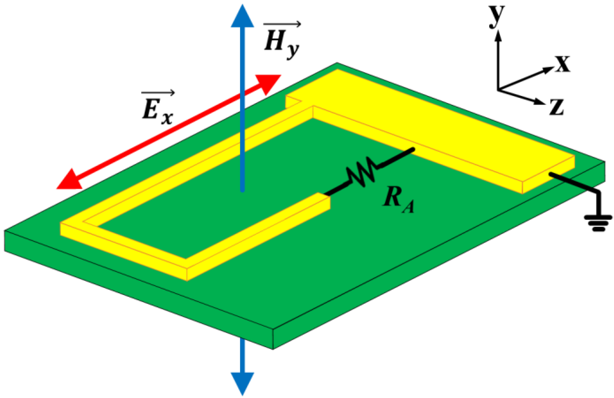
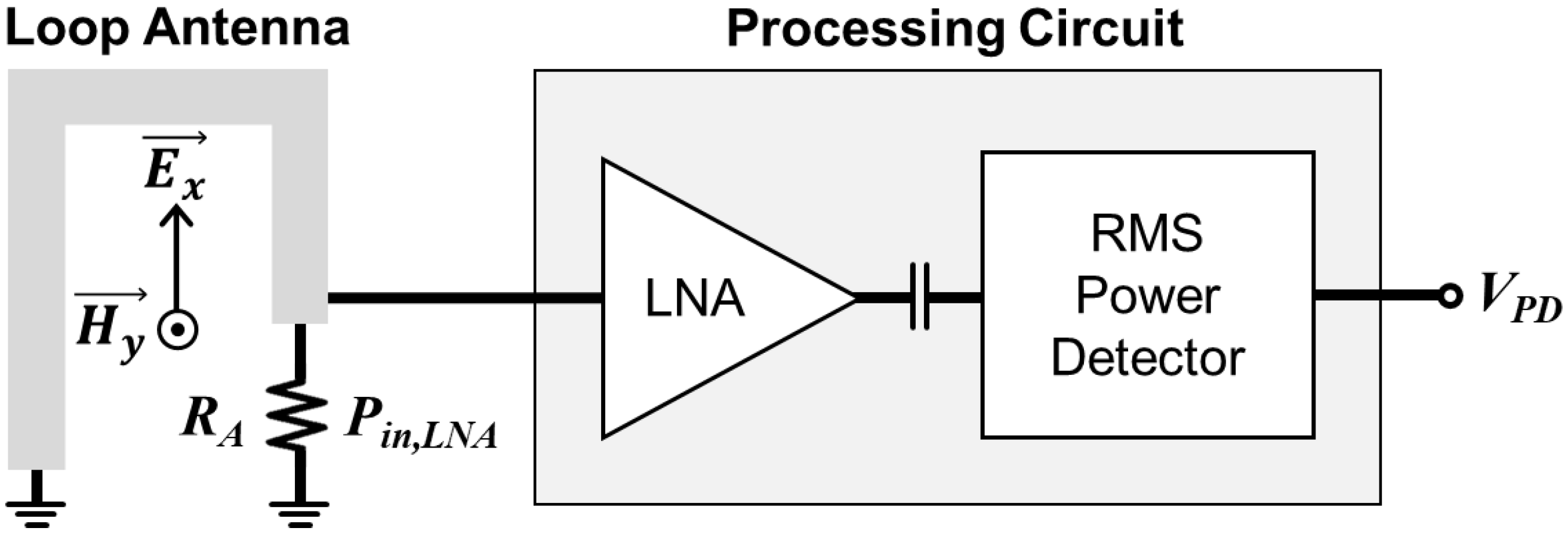
2. Probe Design
2.1. Probe Structure
2.2. Probe Design
2.3. Probe Operation
3. Probe Fabrication and Measurement
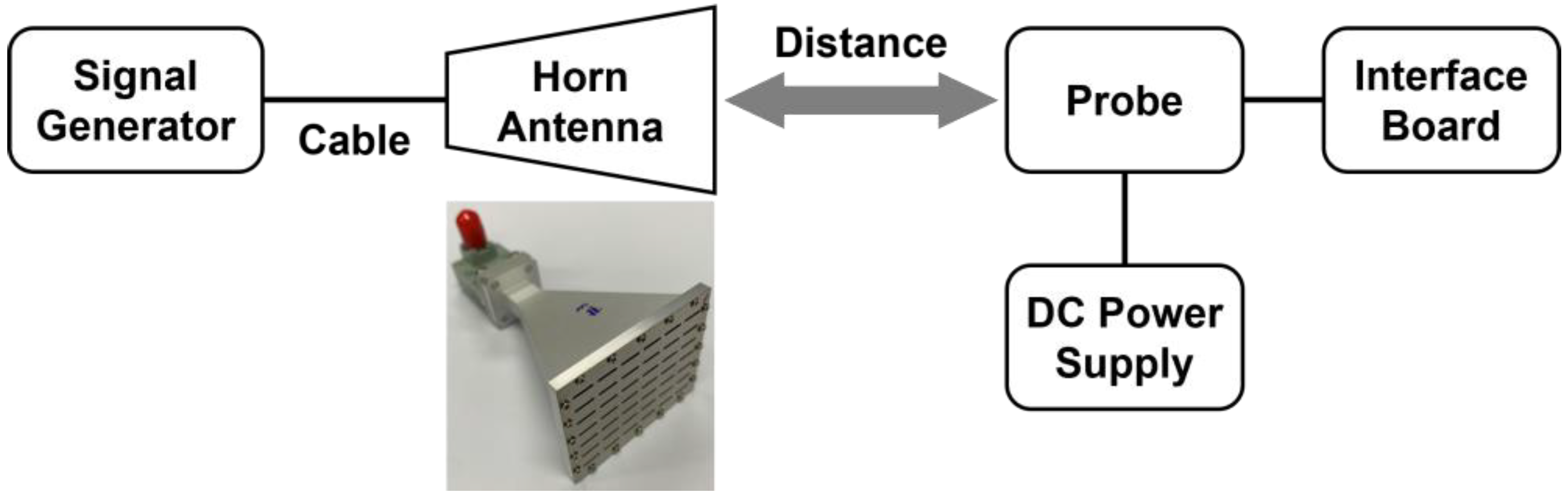
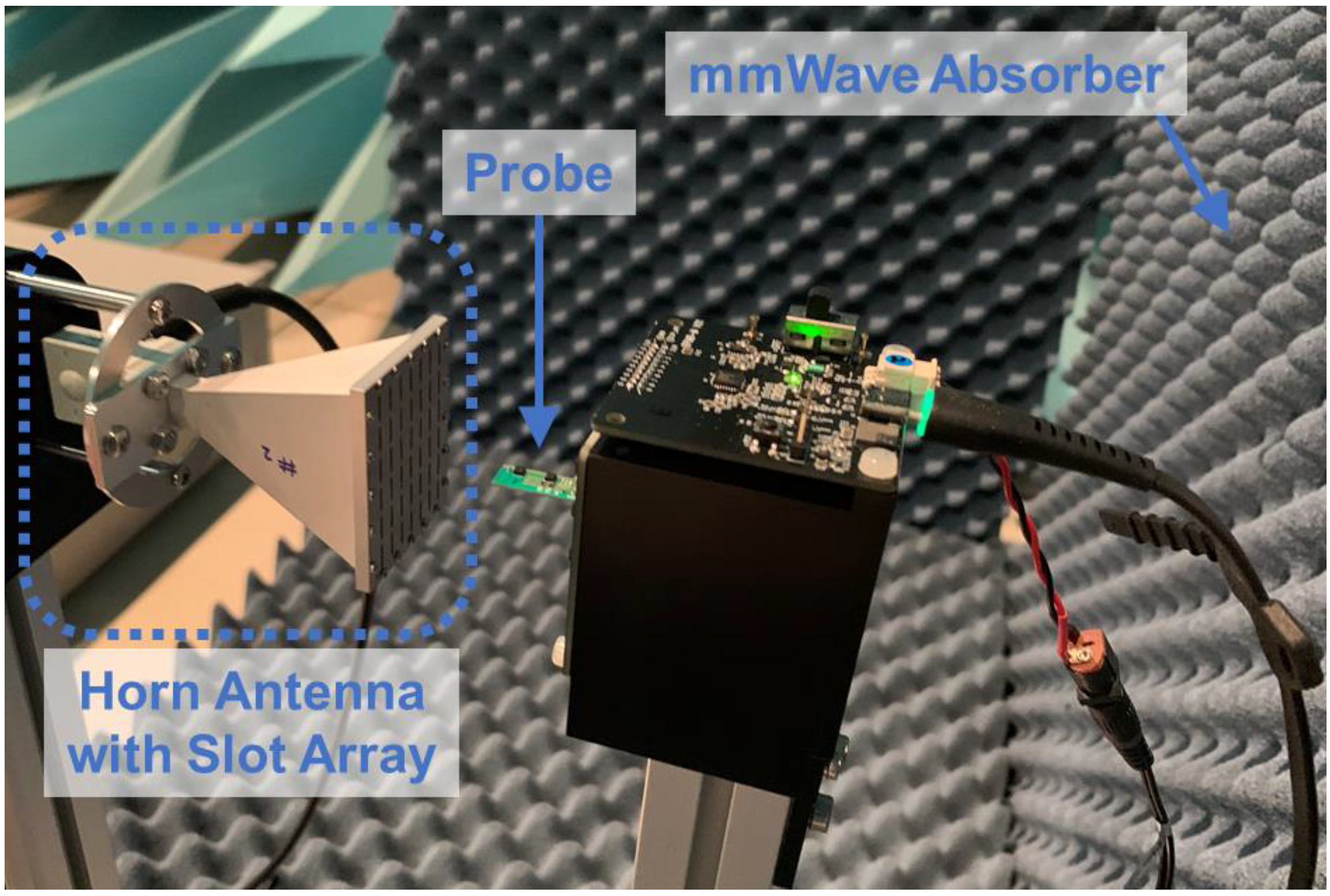
3.1. Fabricated Probe and Measurement Setup
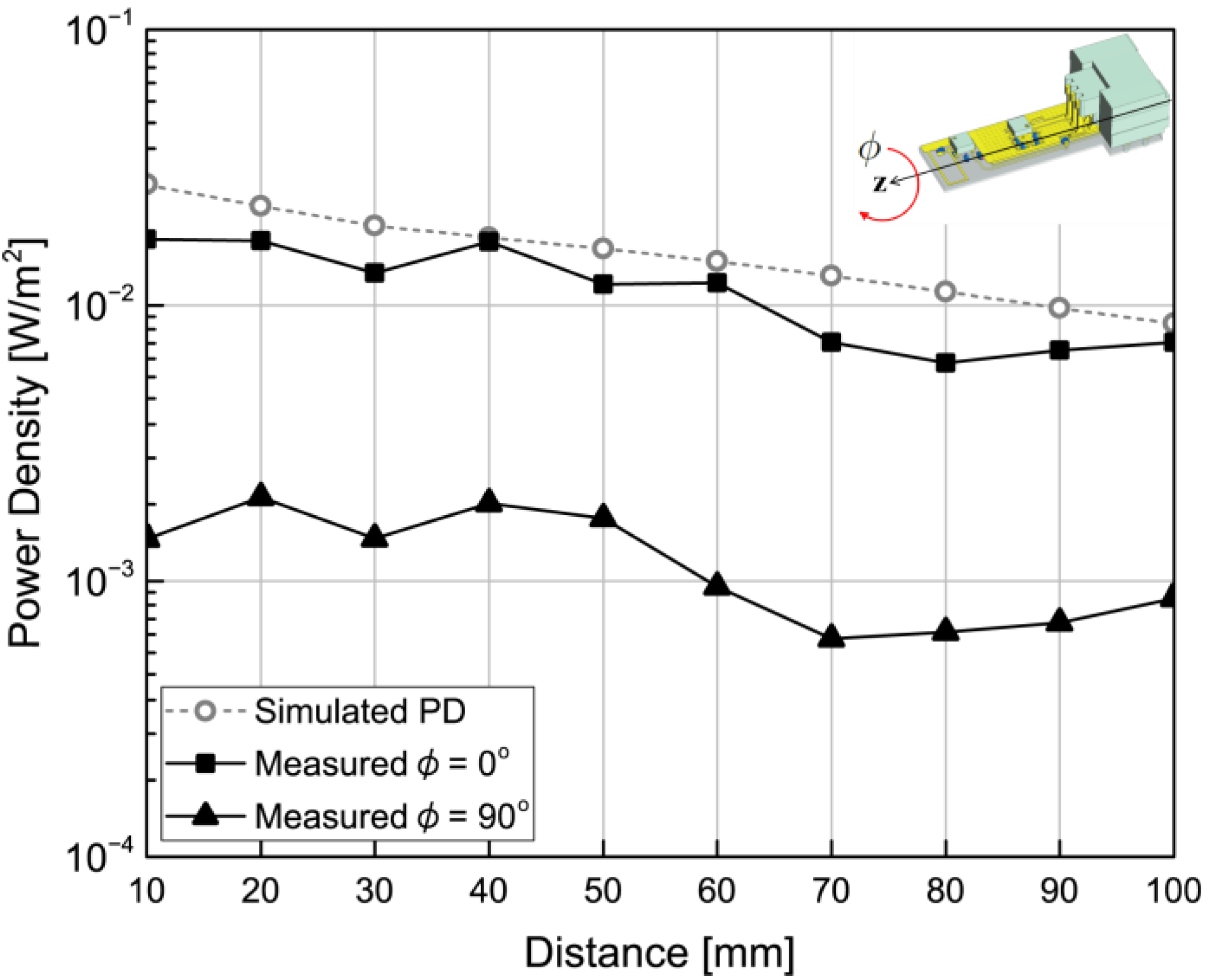
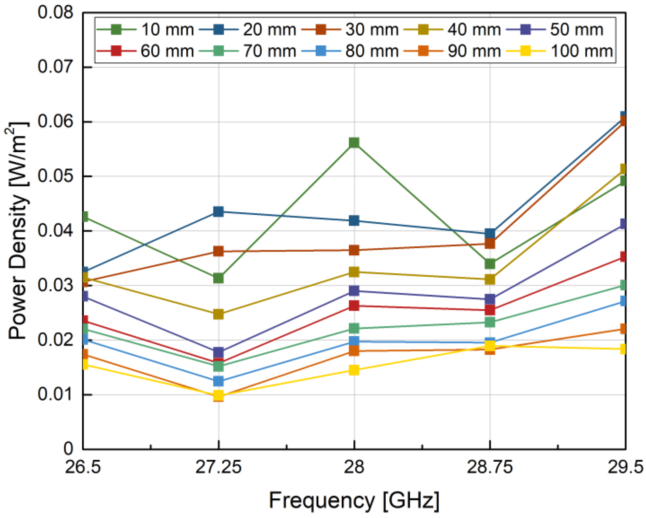
3.2. Measurement Results
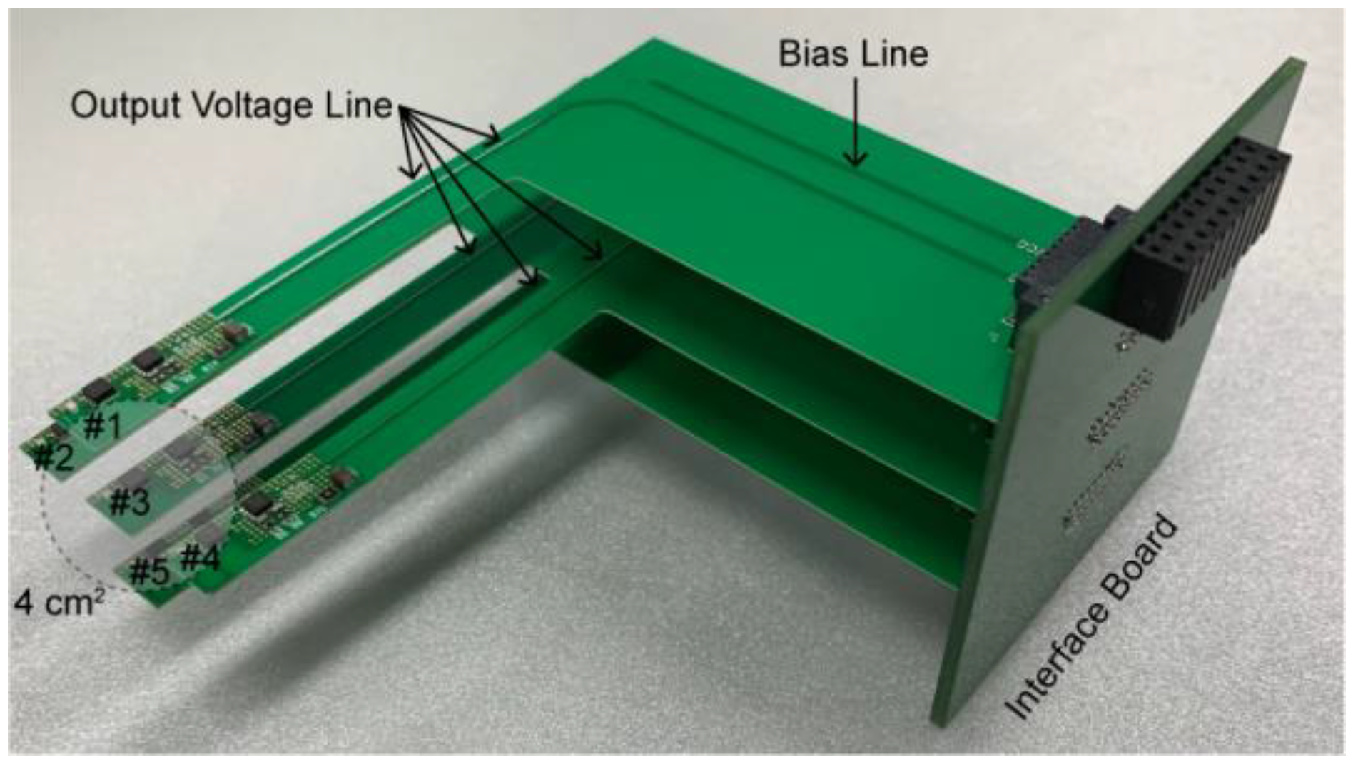
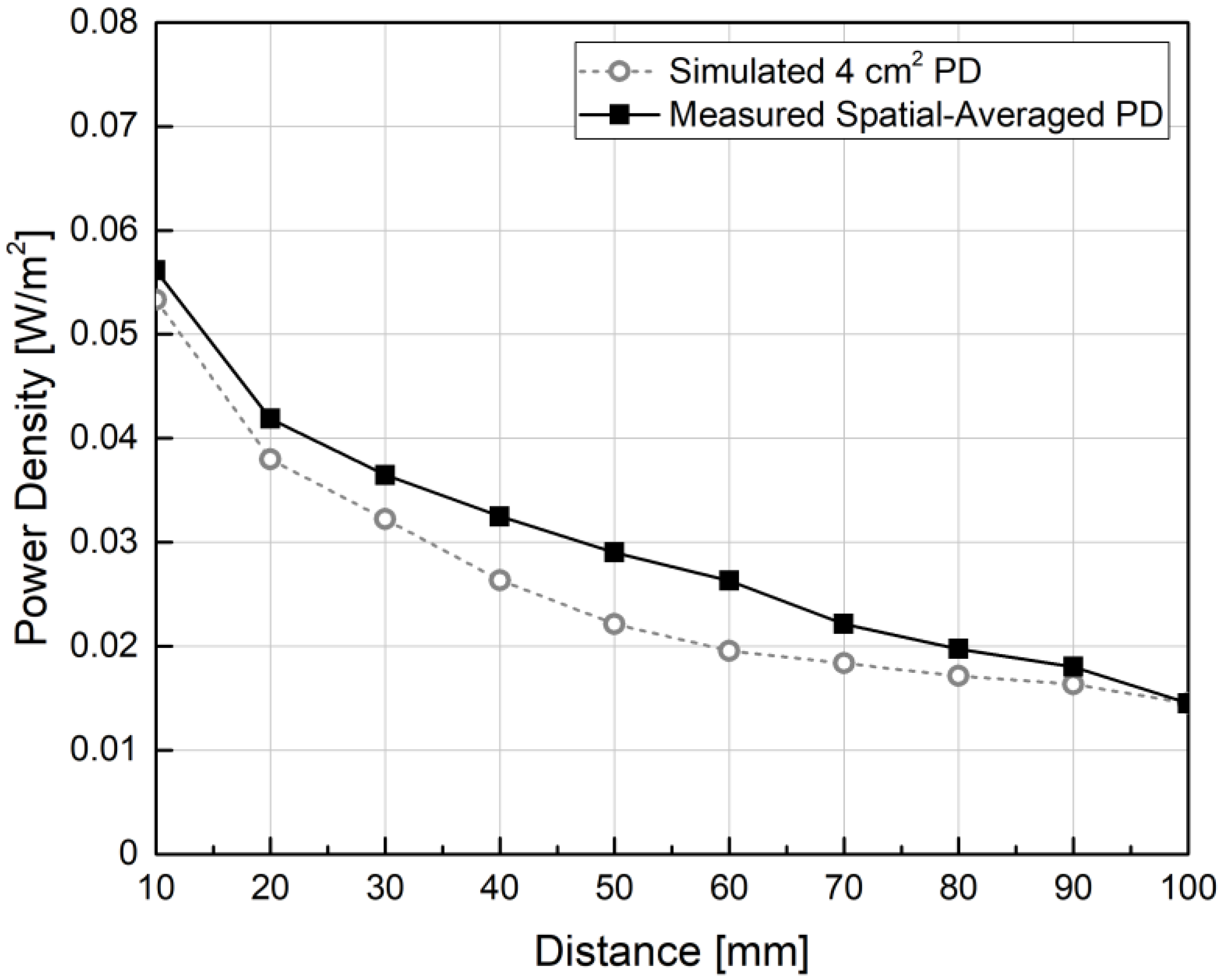
3.3. Expansion to Probe Array
4. Discussion on Reactive near Field Measurement
5. Conclusions
Author Contributions
Funding
Institutional Review Board Statement
Informed Consent Statement
Data Availability Statement
Conflicts of Interest
References
- Aerts, S.; Verloock, L.; Van Den Bossche, M.; Colombi, D.; Martens, L.; Törnevik, C.; Joseph, W. In-situ measurement methodology for the assessment of 5G NR massive MIMO base station exposure at sub-6 GHz frequencies. IEEE Access 2019, 7, 184658–184667. [Google Scholar] [CrossRef]
- Adda, S.; Aureli, T.; D’elia, S.; Franci, D.; Grillo, E.; Migliore, M.D.; Pavoncello, S.; Schettino, F.; Suman, R. A theoretical and experimental investigation on the measurement of the electromagnetic field level radiated by 5G base stations. IEEE Access 2020, 8, 101448–101463. [Google Scholar] [CrossRef]
- Chiaraviglio, L.; Lodovisi, C.; Franci, D.; Pavoncello, S.; Aureli, T.; Blefari-Melazzi, N.; Alouini, M.-S. Massive measurements of 5G exposure in a town: Methodology and results. IEEE Open J. Commun. Soc. 2021, 2, 2029–2048. [Google Scholar] [CrossRef]
- Lee, A.K.; Jeon, S.B.; Choi, H.D. EMF levels in 5G new radio environment in Seoul, Korea. IEEE Access 2021, 9, 19716–19722. [Google Scholar] [CrossRef]
- Kim, K.; Lee, Y.S.; Kim, N.; Choi, H.D.; Lim, K.M. 5G Electromagnetic radiation attenuates skin melanogenesis in vitro by suppressing ROS generation. Antioxidants 2022, 11, 1449. [Google Scholar] [CrossRef] [PubMed]
- Wali, S.Q.; Sali, A.; Allami, J.K.; Osman, A.F. RF-EMF exposure measurement for 5G over mm-wave base station with MIMO antenna. IEEE Access 2022, 10, 9048–9058. [Google Scholar] [CrossRef]
- Colombi, D.; Ghasemifard, F.; Joshi, P.; Xu, B.; Di Paola, C.; Törnevik, C. Methods and practices for in situ measurements of RF EMF exposure from 5G millimeter wave base stations. IEEE Trans. Electromagn. Compat. 2022, 64, 1986–1993. [Google Scholar] [CrossRef]
- International Commission on Non-Ionizing Radiation Protection. Guidelines for Limiting Exposure to Electromagnetic Fields (100 kHz to 300 GHz). Health Phys. 2020, 118, 483–524. [Google Scholar] [CrossRef] [PubMed]
- Feng, Z.; Wang, J.; Diao, Y. Estimation of absorbed power density based on spherical wave expansion to plane wave expansion for exposure assessment at 30 GHz. IEEE Antennas Wirel. Propag. Lett. 2023, 22, 546–550. [Google Scholar] [CrossRef]
- Xing, G.; Li, S.; Hoorfar, A.; An, Q.; Zhao, G. Near-field millimeter-wave imaging via multi-plane MIMO arrays. IEEE Access 2023, 11, 37347–37359. [Google Scholar] [CrossRef]
- IEC TR 63170:2018; Measurement Procedure for the Evaluation of Power Density Related to Human Exposure to Radio Frequency Fields from Wireless Communication Devices Operating between 6 GHz and 100 GHz. Technical Report; International Electrotechnical Commission: Geneva, Switzerland, 2018.
- Kanda, M.; Driver, L.D. An isotropic electric-field probe with tapered resistive dipoles for broad-band use, 100 kHz to 18 GHz. IEEE Trans. Microw. Theory Techn. 1987, 35, 124–130. [Google Scholar] [CrossRef]
- Hwang, J.H.; Kwak, S.I.; Kwon, J.H.; Choi, H.D. Development of multi-band personal dosimeter for RF and ELF exposure monitoring. In Proceedings of the URSI Asia-Pacific Radio Science Conference (URSI AP-RASC), Seoul, Republic of Korea, 21–25 August 2016; pp. 414–416. [Google Scholar]
- Shao, W.; Fang, W.; Huang, Y.; Li, G.; Wang, L.; He, Z.; Shao, E.; Guo, Y.; En, Y.; Yao, B. Simultaneous measurement of electric and magnetic fields with a dual probe for efficient near-field scanning. IEEE Trans. Antennas Propag. 2019, 67, 2859–2864. [Google Scholar] [CrossRef]
- MAAL-011129 Broadband LNA, 18-31.5 GHz. MALCOM. Available online: https://www.macom.com/products/product-detail/MAAL-011129 (accessed on 20 April 2023).
- LTC5596 Datasheet and Product Info: Analog Devices. Linear Technology. Available online: https://www.analog.com/en/products/ltc5596.html#product-overview (accessed on 20 April 2023).
- Kwon, D.; Hwang, J.-H.; Hyoung, C.-H.; Choi, H.-D. A compact rectangular loop antenna for 5G mmWave application. In Proceedings of the International Symposium on Antennas and Propagation (ISAP), Sydney, Australia, 31 October–3 November 2022; pp. 203–204. [Google Scholar]


Disclaimer/Publisher’s Note: The statements, opinions and data contained in all publications are solely those of the individual author(s) and contributor(s) and not of MDPI and/or the editor(s). MDPI and/or the editor(s) disclaim responsibility for any injury to people or property resulting from any ideas, methods, instructions or products referred to in the content. |
© 2023 by the authors. Licensee MDPI, Basel, Switzerland. This article is an open access article distributed under the terms and conditions of the Creative Commons Attribution (CC BY) license (https://creativecommons.org/licenses/by/4.0/).
Share and Cite
Kwon, D.; Lee, Y.S.; Hyoung, C.-H.; Hwang, J.-H.; Choi, H.-D. Loop-Type Field Probe to Measure Human Body Exposure to 5G Millimeter-Wave Base Stations. Appl. Sci. 2023, 13, 11777. https://doi.org/10.3390/app132111777
Kwon D, Lee YS, Hyoung C-H, Hwang J-H, Choi H-D. Loop-Type Field Probe to Measure Human Body Exposure to 5G Millimeter-Wave Base Stations. Applied Sciences. 2023; 13(21):11777. https://doi.org/10.3390/app132111777
Chicago/Turabian StyleKwon, DukSoo, Young Seung Lee, Chang-Hee Hyoung, Jung-Hwan Hwang, and Hyung-Do Choi. 2023. "Loop-Type Field Probe to Measure Human Body Exposure to 5G Millimeter-Wave Base Stations" Applied Sciences 13, no. 21: 11777. https://doi.org/10.3390/app132111777
APA StyleKwon, D., Lee, Y. S., Hyoung, C.-H., Hwang, J.-H., & Choi, H.-D. (2023). Loop-Type Field Probe to Measure Human Body Exposure to 5G Millimeter-Wave Base Stations. Applied Sciences, 13(21), 11777. https://doi.org/10.3390/app132111777