Article

Study of High Transmittance of SiO2/Nb2O5 Multilayer Thin Films Deposited by Plasma-Assisted Reactive Magnetron Sputtering

1
Korea Photonics Technology Institute, Gwangju 61007, Republic of Korea
2
Optrontec, Daejeon 34113, Republic of Korea
*
Author to whom correspondence should be addressed.
Appl. Sci. 2023, 13(24), 13271; https://doi.org/10.3390/app132413271
Submission received: 14 November 2023 / Revised: 7 December 2023 / Accepted: 11 December 2023 / Published: 15 December 2023
(This article belongs to the Special Issue Properties, Characterization and Applications of Ceramics Materials)

Abstract

:
SiO2/Nb2O5 multilayer thin films were designed for the special application of an aviation lighting system emitting green light. For optical components in this system to meet requirements such as a high transmittance and durability, SiO2/Nb2O5 multilayer thin films of 60 individual layers were fabricated by a plasma-assisted reactive magnetron sputtering method. As a result, the transmittance spectra were confirmed to have a flat top surface and a square bandwidth. The transmittances of the SiO2/Nb2O5 multilayer thin films in the range of 500 nm to 550 nm was approximately 96.14%. The reason for high transmittance was attributed to the almost matching between the designed and fabricated SiO2/Nb2O5 multilayer thin films. It was found that there was little difference in the total thickness between the designed and fabricated SiO2/Nb2O5 multilayer thin films without interlayer diffusion. The surface roughness and hardness of the SiO2/Nb2O5 multilayer thin films on a glass substrate was 2.32 nm ± 0.19 nm and 6.6 GPa, respectively. These results indicate that SiO2/Nb2O5 multilayer thin films can be applied not only to the optical filters used in aviation lighting devices, but also to various optics applications because of high transmittance.

1. Introduction

Various optical filters with complex target specifications can be applied to various state-of-art technologies, including the superconducting technology, green energy generation/storage technology, and the emerging 5G networks technology [1]. Optical filters consist of a complex multilayer thin film coating using tens or hundreds of layers made of two or more materials [2]. Among the special application fields using optical filters, taxiway lights helping aircraft to move safely and quickly on the ground must emit green light in accordance with international standards [3]. If the color classification of the lights installed on the runway is not clear, a serious aviation accident may occur. Therefore, it is mandatory to use the aviation lighting system emitting green light.
To meet international standards, optical band pass filters with a high transmittance in the 530 nm wavelength band must be applied. In order to develop an optical band pass filter mounted on taxiway lights among aviation lighting devices, an optical thin film with a transmission performance of more than 95% in the 500~550 nm band was studied. The reliability of lighting devices exposed to the external environment all year round is very important for safety. Therefore, it is very important to select the most durable coating method and materials to produce optical band pass filters with excellent visibility.
SiO2 is well known as a low-refractive-index material in optical multilayer systems because of its wide region of transparency from UV to near-infrared wavelengths and superior environmental resistance [2,4,5,6]. Nb2O5 as a high-refractive-index material has been used instead of the more common TiO2 because of some advantages such as dense microstructures and low optical absorption [7]. To improve its optical properties, Nb2O5 has been selected as a high-refractive-index and low-loss material for optical waveguides, interference filters, and anti-reflection [8]. Nb2O5 as a highly refractive material has been applied by using the plasma-assisted vapor deposition, ion-assisted electron beam evaporation and sputtering methods, etc. [9,10].
In this work, Nb2O5 was selected as a high-refractive-index material and SiO2 was selected as a low-refractive-index material. SiO2/Nb2O5 multilayer thin films were designed using the software Essential Macleod (version 11.8.600) on the basis of characteristics such as refractive index, optical constant, and substrate. Nb2O5 and SiO2 were sputtered to obtain an excellent transmission performance. The structural characteristics of single-layer Nb2O5 and SiO2 thin films deposited by using a magnetron sputtering were analyzed using an X-ray diffractometer (XRD) and X-ray photoelectron spectroscopy (XPS). Surface and cross-sectional images were characterized by using scanning electron microscopy (SEM). The surface roughness of 60 layers of SiO2/Nb2O5 multilayer thin films was evaluated by atomic force microscopy (AFM). The optical transmittance and reflectance of the SiO2/Nb2O5 multilayer thin films was characterized by using a UV–VIS spectrophotometer. Hardness properties of the thin films were measured by using a nanoindenter equipped with a modified Berkovich indenter. The optical transmittance of 60 layers of the SiO2/Nb2O5 multilayer thin films was compared with that of commercial products. Finally, the feasibility of the SiO2/Nb2O5 multilayer thin films was evaluated for application to taxiway lights.

2. Experimental Details

2.1. Fabrication

Multilayer thin films were designed by combining Nb2O5 as a high-refractive-index material and SiO2 as a low-refractive-index material. We designed the SiO2/Nb2O5 multilayer thin films using Essential Macleod with variable parameters such as material, refractive index, extinction coefficient, and wavelength. Nb2O5 and SiO2 layer thicknesses were decided in order to achieve highest transmittances in the range of 500 nm to 550 nm. Each layer’s thicknesses were designed in the range of 40 nm to 120 nm. Single-layer thin films and multilayer thin films composed of SiO2 and Nb2O5 were fabricated by the plasma-assisted reactive magnetron sputtering method in order to improve the durability of thin films. The commercial coating machine (OWLS-1800, Optorun Co., Ltd., Tsurugashima, Japan) was used in the experiment. The coating equipment separates the metal coating region using mid-frequency magnetron sputtering and the oxidation region using radio-frequency inductive coupled plasma. The glass substrates were rotated into two regions repeatedly and finally a metal oxide thin film was densely deposited on the glass substrates. The respective refractive index (n) and extinction coefficient (k) were obtained using the SiO2 (1250 nm) and Nb2O5 (600 nm) single-layer thin films on three glass substrates (B33, D263, and D270, Schott AG). The SiO2/Nb2O5 multilayer thin films were designed by the number of layers, thickness, and sequence of layers in order to achieve a high transmittance at a central wavelength of 530 nm. The SiO2/Nb2O5 multilayer thin films were prepared by the plasma-assisted reactive magnetron sputtering method. A multi-target apparatus was used for the deposition process using the parameters listed in Table 1. The base pressure (Pa) and working pressure (Pa) were 2.0 × 10⁻⁵ and 8.0~9.0 × 10⁻¹. The deposition rate (Å/s) of SiO2 and Nb2O5 was 6.2~9.29 (Å/s) and 1.67~4.76(Å/s), respectively. Various deposition conditions such as power supplied to the magnetron, deposition rate, and sputtering time were precisely controlled.

2.2. Characterization

The amorphous nature of the SiO2/Nb2O5 multilayer thin films was evaluated by means of an X-ray diffractometer (X’pert Pro, Panalytical) with CuKα (=1.542 Å) used as a source. X-ray photoelectron spectroscopy (NEXSA, Thermo Fisher Scientific) studies were carried out to determine the chemical states of the niobium, silicon, and oxygen at the surface of the SiO2/Nb2O5 multilayer thin films. The coefficient of thermal expansion of the substrates was measured using a dilatometer (DIL402F3, NETZSCH, Selb, Germany) in the range of 0–450 °C with a heating rate of 5 °C/min. under a N2 atmosphere. The surface morphology and elemental compositions of the SiO2/Nb2O5 multilayer thin films were characterized using scanning electron microscopy (SU8100, Hitachi, Tokyo, Japan). The surface roughness of the thin film was measured using an atomic force microscope (Bruker, Billerica, MA, USA), which yielded the quantitative root mean square (RMS) value for the SiO2/Nb2O5 multilayer thin films. The transmittance spectra were recorded by a UV–Vis spectrophotometer (Cary 500 scan, Varian H) within 480–600 nm. The commercial thin films substrates were purchased from Edmund (ED) and Isuzu (IS) as a reference sample. The hardness of the thin films was characterized by a nanoindenter with a Berkovich tip (SteP6 UNHT3, Anton Paar, Graz, Austria). A spectroscopic ellipsometer (M2000, J.A. Woollam, Lincoln, USA) was used to measure the refractive index (n) of the single-layer SiO2 and Nb2O5 thin films. Nano-indentation tests were conducted seven times and the average values were obtained. The Oliver–Pharr method was used to calculate the hardness of the thin films. The penetration depth of indentation was determined within 10% of the thin-film thickness to minimize the influence of the substrates [4].

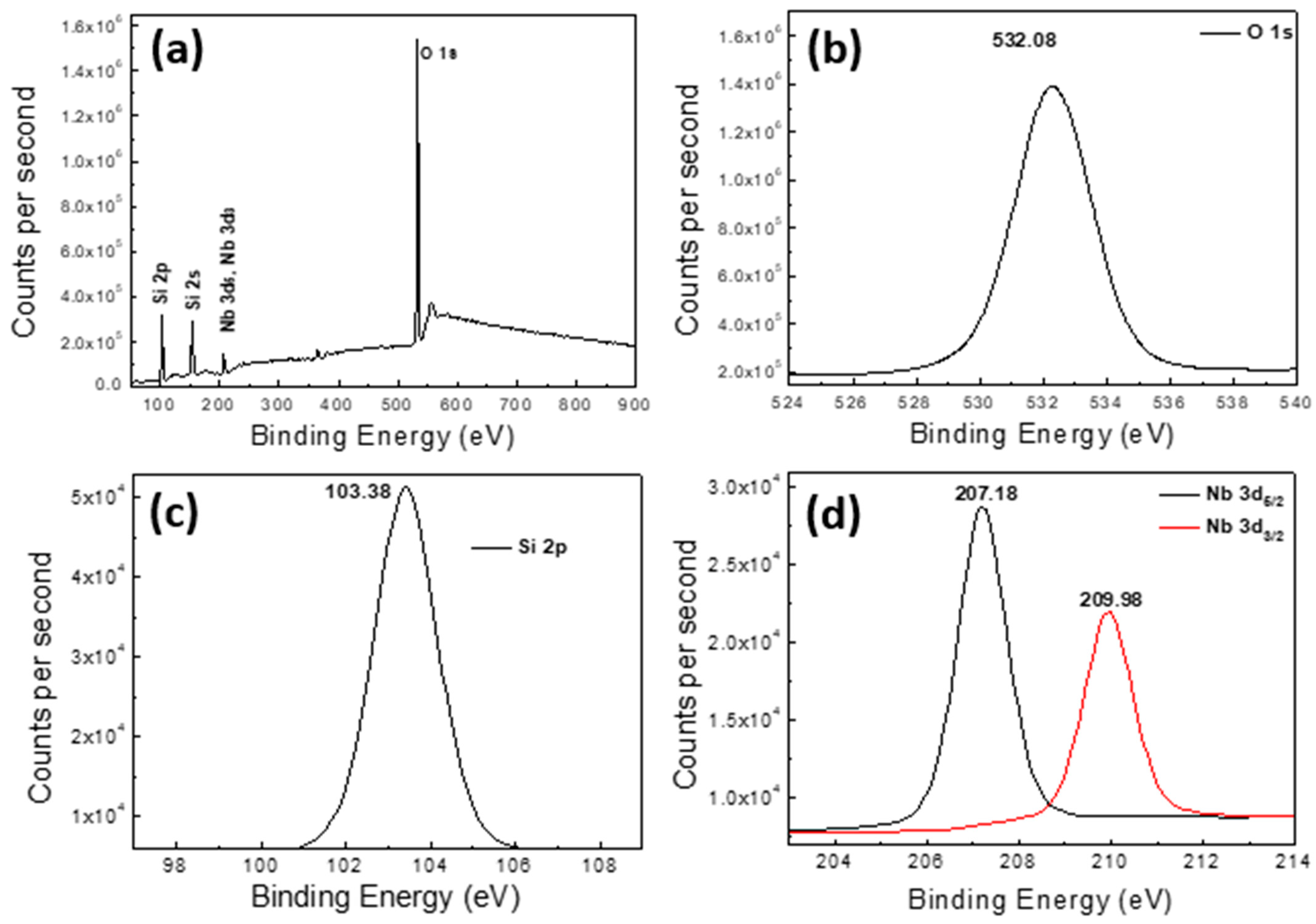
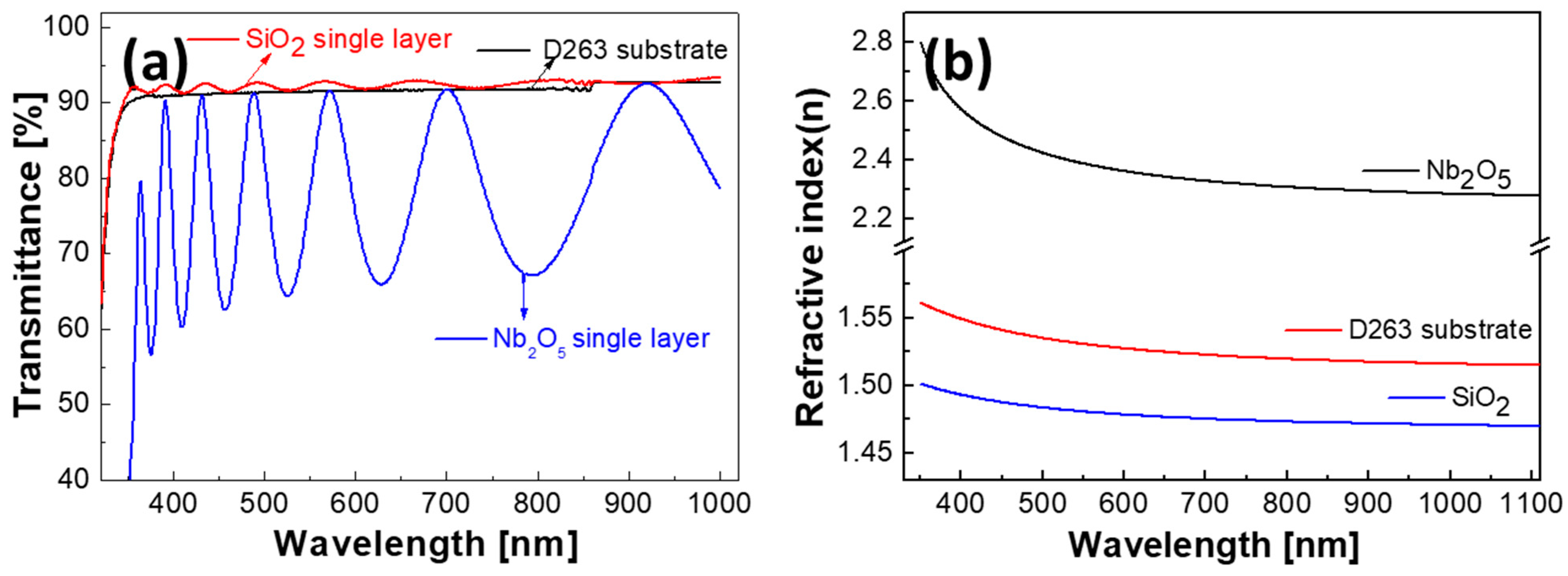
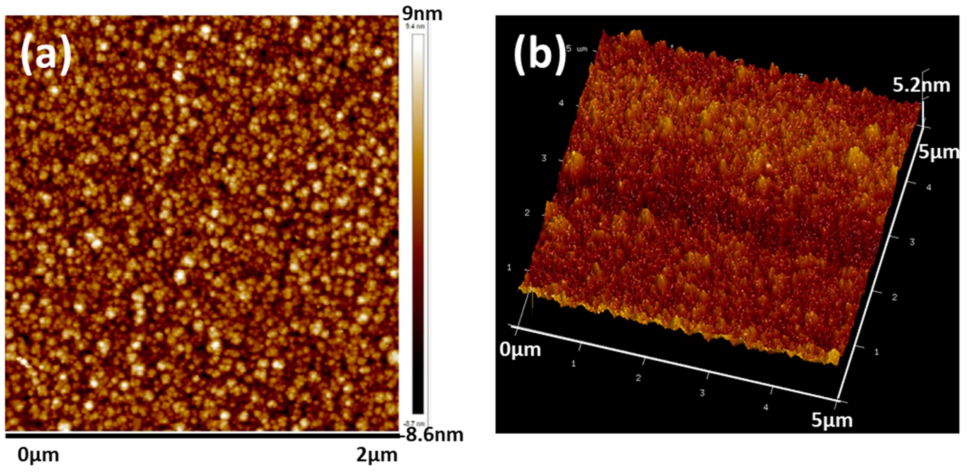
3. Results and Discussion

Three substrates (B33, D263, and D270) from Schott were used to evaluate the compatibility of the thin-film growth for multilayer thin films. They have very similar optical properties such as transmittance and refractive index. However, the coefficients of thermal expansion in the 25~300 °C range are 3.3, 7.2, and 9.4 (×10−6/K), respectively. The SiO2/Nb2O5 multilayer thin films were deposited onto these three substrates (B33, D263, and D270) using the sputtering deposition conditions listed in Table 1. Typical XRD patterns of the SiO2/Nb2O5 multilayer thin films on the three substrates are shown in Figure 1. The SiO2/Nb2O5 multilayer thin films were amorphous regardless of the substrate types. The amorphous peak was located at 2θ~25° in the XRD pattern. The XRD patterns representing SiO2 and Nb2O5 crystal phases did not appear, indicating that the multilayer thin films were homogeneous and isotropic. Other studies on SiO2/Nb2O5 multilayer thin films deposited by an e-beam or sputtering methods show similar results [4,11,12]. The coefficients of thermal expansion of the film materials SiO2 and Nb2O5 were 0.55 and 5.8 (×10−6/K), respectively [13]. Based on the results, D263 was used in this current work in order to minimize the strain and stress between the substrate and thin films since the coefficient of thermal expansion 7.2 (×10−6/K) of D263 is close to 5.8 (×10−6/K) of Nb2O5 [14].
The SiO2/Nb2O5 multilayer thin films were analyzed using X-ray photoelectron spectroscopy (XPS, NEXSA, Thermo Fisher Scientific, Waltham, MA, USA) to analyze the binding energy and chemical composition of the SiO2 and Nb2O5. During XPS analysis, the pressure was maintained at 1.5 × 10⁻⁹ Torr, and Al Kα (hν = 1486.6 eV) was used as the X-ray light source. As shown in Figure 2a, the full spectrum of XPS confirms the presence of Si, O, and Nb on the surface of the SiO2/Nb2O5 multilayer thin films. It was confirmed that within the SiO2 and Nb2O5 optical thin-film layers, major peaks assigned to O1s, Si2p, Si2s, Nb3d5/2, and Nb3d3/2 are distinctive indicating the respective components. It is not easy to determine the exact valence state in silicon oxide and niobium oxide thin film. In this study, we aim to compare SiO2/Nb2O5 multilayer thin films with previous research reports. In fact, the amorphous oxide thin films are nonstoichiometric. Si2p peak was formed at 103.38 eV and the O1s spectra were located at 532.08 eV as shown in Figure 2b,c. Alfonsetti et al. reported the different oxygen concentration in SiOx as a function of Si2p binding energy. The behavior of the Si2p was shifted from 101.9 eV to 103.8 eV as the oxygen concentration increased from x = 1.05 to 2 in SiOx [15]. Ingo et al. reported that the binding energies of Si2p and O1s are 103.4 and 533.0 eV, respectively [16]. Based on comparisons with the above references, the current results obtained from Figure 2b,c reflect that the binding energies of Si4+ and O2− are combined in the form of SiO2. The doublet with binding energies ~207.18 (Nb3d5/2) and ~209.98 eV (Nb3d3/2) was associated with photoelectrons emitted from Nb atoms as shown in Figure 2d. Other studies reported that three XPS peaks are assigned to Nb2O5, NbO2, and NbO, which are located at ~208.6 eV, 206.2 eV, and 203.6 eV [17]. King et al. reported that the niobium spectra broaden and shift to a lower binding energy, indicating the presence of multiple oxidation states, i.e., Nb4 + (208.6, 205.9 eV) and Nb2+ (206.6, 203.9 eV) [18]. Lombardo et al. reported that the doublet at binding energy 207.1 eV (Nb3d5/2) is characteristic of the Nb5+ state, and the peak at 209.8 eV (Nb3d3/2) also confirms the film composition as diniobium(V) pentoxide, Nb2O5. The binding energies ~207.18 (Nb3d5/2) and ~209.98 eV (Nb3d3/2) from the current XPS spectrum were very similar to the reported results, i.e., characteristic peaks at 209.8~209.9 eV (Nb3d3/2) and 207.1~207.2 eV (Nb3d5/2) indicating the presence of Nb5+ [18,19]. Thus, the above XPS results indicated the major presence of Si4+ and Nb5+ in the SiO2/Nb2O5 multilayer thin films. Although the ratios are substoichiometric for both silicon and niobium, they are written as simplified SiO2/Nb2O5 multilayer thin films in the paper.
In order to investigate the optical parameters, single-layer SiO2 and Nb2O5 thin films on a D263 substrate were prepared. The refractive index was compared using a UV–Vis spectrophotometer and spectroscopic ellipsometer. Figure 3a shows the transmittance of the single-layer SiO2 and Nb2O5 thin films by using a UV–Vis spectrophotometer. Essential Macleod was used to calculate the refractive index (n) from the spectral data of the UV–Vis spectrophotometer. The measured refractive index (n) of the single-layer SiO2 and Nb2O5 thin films obtained were 1.481 and 2.398 at 530 nm, respectively. Figure 3b shows the refractive index (n) of the single-layer SiO2 and Nb2O5 thin films, as well as a D263 substrate measured by using a spectroscopic ellipsometer. The refractive index (n) and extinction coefficient (k) were calculated from spectra fits on the basis of a Lorentzian multi-oscillator model [20]. The measured refractive index (n) of the single-layer SiO2 and Nb2O5 thin films at 530 nm were 1.468 and 2.404, respectively. The extinction coefficient (k) of the single-layer Nb2O5 thin films at 530 nm was 1.0 × 10⁻⁵. According to two methods, the difference of refractive index (n) of the single-layer SiO2 and Nb2O5 thin films were 0.87% and 0.25%, respectively. SiO2/Nb2O5 multilayer thin films were designed with Essential Macleod using the refractive index (n) of the single-layer SiO2 and Nb2O5 thin films measured on a spectroscopic ellipsometer. The refractive index of the SiO2 thin film was similar to the refractive index of quartz (bulk SiO2). Tajima et al. reported a refractive index of 1.47 at 540 nm for a SiO2 optical thin film deposited by the DC sputtering method [21]. The refractive index values of Nb2O5 thin films deposited by sputtering methods were previously reported according to processing conditions and film thickness to be in the range of 2.14 to 2.44 at 530 nm [10,22]. It is well known that the refractive index of optical thin films by the sputtering methods is higher than that of optical thin films by electron beam deposition methods. This indicates that the thin films deposited by sputtering methods are denser than the films prepared by electron beam deposition methods [23,24]. In this work, single-layer SiO2 and Nb2O5 thin films deposited by the plasma-assisted reactive magnetron sputtering method indirectly show that a deposition process to obtain dense and durable thin films has been secured.
Figure 4a shows cross-sectional and surface SEM images of the SiO2/Nb2O5 multilayer thin films deposited by plasma-assisted reactive magnetron sputtering method on D263 substrates. The secondary electron (SE) image clearly shows 60 individual layers of alternating SiO2 and Nb2O5, since Nb has a higher atomic number than that of Si. The measured thickness of dark SiO2 layers with a low index and bright Nb2O5 layers with a high index is almost matching with the thickness designed with Essential Macleod. There was little difference in the total thickness between the designed and fabricated SiO2/Nb2O5 multilayer thin films. The total thickness of the designed and fabricated thin films was 6.03 μm and 6.10 μm, respectively. Interfacial diffusion among thin films was not observed between each SiO2 and Nb2O5 layer. Hence, by constructing SiO2/Nb2O5 multilayer thin films properly, one can reduce the cross-plane scattering without deterioration in band pass filtering. The surface with a grain boundary of 50 to 200 nm in size was observed on the top surface as shown in Figure 4b. Overall, a very smooth and flat surface was obtained.
A cross-sectional image of 12 layers of the SiO2/Nb2O5 thin films is displayed, where white indicates energy dispersive X-ray spectroscopy (EDS) line scanning, as shown in Figure 5a. EDS was used to indicate major elements composed of multilayer thin films. The EDS results showed Nb and Si elements and a small amount of other elements from the substrate. In order to represent the distribution of Nb and Si elements layer by layer, a small percentage of elements were ignored. The distribution results from the EDS line scan were displayed as shown in Figure 5b for the SiO2/Nb2O5 multilayer thin films along the white solid line. The complementary EDS intensity of SiO2 and Nb2O5 is attributed to Si Kα1 and Nb Lα1. The line profiles show alternating sawtooth shapes. The relative contrast changes are reliable and clear periodic oscillations are observed from complementary elemental line profiles. In the Si-rich band, that is, the Nb-deficient region, the EDS intensity of Si Kα1 was relatively high, in contrast to Nb Lα1, and conversely the EDS intensity for Nb Lα1 was relatively high in the Nb-rich region. It was shown that there was a clear distinction between the Si and the Nb thin-film layer, indicating that the multilayer thin film was successfully manufactured without observable interfacial diffusion.
AFM measurements were performed in order to confirm the information regarding the surface topography of the as-prepared thin films. The 2D and 3D topography of the SiO2/Nb2O5 multilayer thin films shows smooth surfaces, as presented in Figure 6. The calculated root mean square (RMS) surface roughness was found to be equal to 2.32 nm ± 0.19 nm. A crack-free, densely packed surface was obtained and this was also confirmed by the SEM topography results presented in Figure 4. It is well known that the sputtering method has advantages for obtaining dense and uniform structures because the surface diffusion of sputtered substrates promotes the growth of a homogenous film [25,26]. Using the sputtering method, many studies have been conducted to improve surface roughness according to sputtering power, process pressure, etc. AFM images of the TiO2 thin film and SiO2 thin film presented surface roughness in the range of RMS 0.84~1.04 nm using a sputtering power of 8.1 kW and 6.0 kW, respectively [27]. A similar study reported antireflection films with an Air/SiO2/Nb2O5/SiO2/Nb2O5/SiO2/Nb2O5/glass structure designed by the Macleod program manufactured by a DC sputtering system. As the process pressure decreased, the surface roughness tended to decrease from 1.242 nm to 0.127 nm [28]. Kwon et al. reported Nb2O5/SiO2/ITO multilayer films prepared using a magnetron sputtering system. The surface roughness of Nb2O5/SiO2/ITO multilayer films was in the range of 0.1~0.4 nm [29]. The current results indicate that the surface condition of SiO2/Nb2O5 multilayer thin films with a 2.32 nm ± 0.19 nm of surface roughness will not deteriorate the optical properties such as transmittance.
SiO2/Nb2O5 multilayer thin films were designed and manufactured based on information such as the refractive index (n) and an extinction coefficient (k) of SiO2 and Nb2O5 with the Essential Macleod program. For the application of multilayer thin films to narrow band pass filters, a square bandwidth of the transmittance is essential at a specific wavelength of 500~550 nm. The application of multilayers, with the thickness of each layer being one-fourth of the wavelength, can improve the performance of an AR (anti reflecting) coating. The high transmittance or high reflection at a specific wavelength using multilayer thin films can be explained by the difference in the refractive index between SiO2 and Nb2O5 [30,31,32]. The optical transmittance and reflectance of the SiO2/Nb2O5 multilayer thin films deposited were characterized using a UV–Visible spectrometer, as shown in Figure 7a. The transmittances of the SiO2/Nb2O5 multilayer thin films in the range of 500 nm to 550 nm were approximately 96.14% in this work. The transmittances of ED and IS commercial thin films in the 500~550 nm range were 91.44% and 84.99%, respectively, as shown in Figure 7b. As a result of comparing the transmittance of the current work with those of the commercial products in the 500 to 550 nm range, the difference in the transmittance of the commercial thin films from ED and IS company was 4.7 and 11.15%, respectively. The thin film of ED, composed of SiO2 and Ta2O5 (refractive index 2.1476 @ 530 nm), has a total thickness of 9.15 μm with approximately 130 layers. The total thickness of the IS thin film, which is composed of SiO2 and TiO2 (refractive index 2.5414 @ 530 nm), is 2.60 μm with approximately 36 layers. In particular, it was confirmed that the deviation of transmittance in the 500 to 550 nm range was more than 5%. In this work, high transmittance was attributed to the flat top surface and square bandwidth, as shown in Figure 7. As explained in Figure 4, there was almost no difference in the thickness of each SiO2, Nb2O5 layer of the designed and fabricated SiO2/Nb2O5 multilayer thin films. Additionally, no significant interfacial diffusion was observed between the SiO2 and Nb2O5 layers.
Hardness (H) is defined as the resistance to local plastic deformation. The Berkovich indenter has a very flat profile and has the same projected area-to-depth ratio as a Vickers indenter. Hardness (Pmax/Ap2) can be explained as the maximum indentation load Pmax divided by the projected contact area Ap. The projected contact area Ap can be estimated from this relationship (Ap = Co × hc2), where Co is 24.6 for the Berkovich indenter and hc is the contact depth [33]. The hardness properties of a thin film can be measured by using a nano indenter equipped with a modified Berkovich indenter. The Oliver–Pharr method using the obtained load vs. displacement curve was used to calculate the hardness of the thin films [34]. Since thin films are very soft compared with substrate materials, an accurate hardness evaluation of thin film is difficult to attain due to the substrate effect. Therefore, it is recommended that the penetration depth of indentation should be within 10% of the thin-film thickness to minimize the influence of the substrate [35]. Figure 8a shows the load–penetration depth curve of a SiO2 and Nb2O5 single-layer thin film on D263 substrates. The load–penetration depth curve was obtained as the corresponding peak load was held for 15 sec at the maximum penetration depth (Hmax). After being unloaded, the penetration depth was not completely recovered, which indicates irreversible plastic deformation in the SiO2 and Nb2O5 single-layer thin films. It was observed that the Pmax reached 3 mN and 0.711 mN for the SiO2 single layer with 600 nm thickness and the Nb2O5 single layer with 1200 nm thickness, respectively. The hardness of the SiO2 and Nb2O5 single-layer thin films was 10.73 GPa and 6.3 GPa, respectively. Previous works on the hardness of SiO2 and Nb2O5 thin films reported a hardness in the ranges of 10.4~11.9 GPa and 6.5~6.8 GPa, respectively [33,36]. The hardness (6.6 GPa) of the SiO2/Nb2O5 multilayer thin films on B33 substrates showed a value that was more than 30% greater than the hardness (4.4 GPa) of the SiO2/Nb2O5 multilayer thin film on D263 substrates. The load–penetration depth curves of the SiO2/Nb2O5 multilayer thin film with 6.09 μm thickness on the B33 and D263 substrates are plotted in Figure 8b. A Pmax of 20 mN was applied for SiO2/Nb2O5 multilayer thin films on the B33 and D263 substrates. The contact depth Hc for SiO2/Nb2O5 multilayer thin films on the B33 and D263 substrates was 280 nm and 332.6 nm, respectively. It is interesting that the same multilayer has different mechanical properties depending on the types of substrate. To investigate the effect of the substrates on the mechanical properties of the multilayer thin films, the physical properties of the substrates were investigated. For the B33 and D263 glass substrates from Schott, the coefficients of mean linear thermal expansion α (20~300 °C) were 3.2 (×10−6/K) and 7.2 (×10−6/K), respectively. This implied that differences in the physical properties of the substrate, represented by linear thermal expansion, affect the physical properties of the thin films. More studies will be conducted systematically to identify the physical factors that directly affect hardness.

4. Conclusions

For the special application of an aviation lighting system emitting green light, optical thin films made of SiO2 and Nb2O5 were designed using Essential Macleod. SiO2/Nb2O5 multilayer thin films were fabricated by the plasma-assisted reactive magnetron sputtering method. An XRD analysis revealed that SiO2/Nb2O5 multilayer thin films have an amorphous phase. Interfacial diffusion was not observed between the SiO2 and Nb2O5 layers based on cross-sectional SEM images and XPS scan spectra showing distinctive major peaks representing O1s, Si2p, Si2s, Nb3d5/2, and Nb3d3/2. XPS results indicated the major presence of Si4+ and Nb5+ in the SiO2/Nb2O5 multilayer thin films, although the ratios were substoichiometric for both silicon and niobium. The most notable results were that the SiO2/Nb2O5 multilayer thin films had a surface roughness of 2.32 nm ± 0.19 nm, determined by an AFM analysis, and a transmittance of 96.14% in the range of 500 nm to 550 nm with a flat top surface and square bandwidth. The hardness of the SiO2/Nb2O5 multilayer thin film on B33 substrates measured by using a nanoindenter was 6.6 GPa. The high transmittance and hardness of the SiO2/Nb2O5 multilayer thin films clearly demonstrate their feasibility for the special application of an aviation lighting system emitting green light.

Author Contributions

Investigation, J.-H.I., S.H.K., K.H., D.L., Y.S.H. and K.M.L.; Writing—original draft, S.K.; Writing—review & editing, J.H.C. All authors have read and agreed to the published version of the manuscript.

Funding

This research was supported by the Materials and Components Technology Development Program of MOTIE/KEIT, 20018828 (Development of optical filter for wavelength control and light source module for lighting device), the Industrial Infrastructure Program for Smart Specialization of MOTIE/KIAT, P0017725 (Project of Industry supporting optical materials for camera lenses), and the Nano and Material Technology Development Program through the National Research Foundation of Korea (NRF), funded by the Ministry of Science and ICT (NRF-2022M3H4A3085283).

Institutional Review Board Statement

Not applicable.

Informed Consent Statement

Not applicable.

Data Availability Statement

Data is contained within the article.

Conflicts of Interest

Author Yun Sik Hwang and Kyung Min Lee were employed by the company Optrontec. The remaining authors declare that the research was conducted in the absence of any commercial or financial relationships that could be construed as a potential conflict of interest.

References

  1. Mbam, S.O.; Nwonu, S.E.; Orelaja, O.; Nwigwe, U.S.; Gou, X.F. Thin-film coating; historical evolution, conventional deposition technologies stress state micro nano level measurement. Mater. Res. Express 2019, 6, 122001. [Google Scholar] [CrossRef]
  2. Sullivan, B.T.; Clarke, G.A.; Akiyama, T.; Osborne, N.; Ranger, M.; Dobrowolski, J.A.; Howe, L.; Matsumoto, A.; Song, Y.; Kikuchi, K. High-rate automated deposition system for the manufacture of complex multilayer coatings. Appl Opt. 2000, 39, 157–167. [Google Scholar] [CrossRef] [PubMed]
  3. ICAO (International Civil Aviation Organization). Annex 14, Standards and Aerodrome Certification; ICAO: Montreal, QC, Canada, 2022. [Google Scholar]
  4. Moriizumi, Y.; Honma, H.; Takai, O. Optical properties and durability performance of substance SiO2/Nb2O5 for multilayer thin films prepared by high-density plasma-assisted vapor deposition. Jpn. J. Appl. Phys. 2016, 55, 01AA23. [Google Scholar] [CrossRef]
  5. Thielsch, R.; Gatto, A.; Heber, J.; Kaiser, N. A comparative study of the UV optical and structural properties of SiO2, Al2O3, and HfO2 single layers deposited by reactive evaporation, ion-assisted deposition and plasma ion-assisted deposition. Thin Solid Film. 2002, 410, 86–93. [Google Scholar] [CrossRef]
  6. Jasapara, J.; Nampoothiri, A.V.V.; Rudolph, W.; Ristau, D.; Starke, K. Femtosecond laser pulse induced breakdown in dielectric thin films. Phys. Rev. 2001, 63, 045117. [Google Scholar] [CrossRef]
  7. Song, Y.; Sakurai, T.; Maruta, K.; Matusita, A.; Matsumoto, S.; Saisho, S.; Kikuchi, K. Optical and structural properties of dense SiO2, Ta2O5 and Nb2O5 thin-films deposited by indirectly reactive sputtering technique. Vacuum 2000, 59, 755–763. [Google Scholar] [CrossRef]
  8. Szymanowski, H.; Zabeida, O.; Klemberg-Sapieha, J.E.; Martinu, L. Optical properties and microstructure of plasma deposited Ta2O5 and Nb2O5 films. J. Vac. Sci. Technol. 2005, 23, 241–247. [Google Scholar] [CrossRef]
  9. Yoshimura, K.; Miki, T.; Iwama, S.; Tanemura, S. Characterization of niobium oxide electrochromic thin films prepared by reactive d.c. magnetron sputtering. Thin Solid Film. 1996, 281/282, 235–238. [Google Scholar] [CrossRef]
  10. Chen, K.N.; Hsu, C.M.; Liu, J.; Liou, Y.C.; Yang, C.F. Investigation of Antireflection Nb2O5 Thin films by the sputtering method under different deposition parameters. Micromachines 2016, 7, 151. [Google Scholar] [CrossRef]
  11. Yuan, Z.S.; Jhang, J.M.; Yu, P.H.; Jiang, C.M.; Huang, Y.C.; Wu, Y.L.; Lin, J.J.; Yang, C.F. Comparisons of theoretical and experimental results of blue light SiO2–Nb2O5 distributed bragg reflector fabricated using E-beam deposition. Vacuum 2020, 182, 109782. [Google Scholar] [CrossRef]
  12. Moriizumi, Y.; Honma, H.; Takai, O. Optical and mechanical properties of SiO2 and Nb2O5 thin films deposited by high-density plasma assisted vapor deposition. J. Surf. Finish. Soc. Jpn. 2015, 66, 212–218. [Google Scholar] [CrossRef]
  13. Chen, T.C.; Chu, C.J.; Ho, C.H.; Wu, C.C.; Lee, C.C. Determination of stress-optical and thermal-optical coefficients of Nb2O5 thin film material. J. Appl. Phys. 2007, 101, 043513. [Google Scholar] [CrossRef]
  14. Shaaban, K.H.; Yousef El, S.; Abdel Wahab, E.A.; Shaaban, S.A.; Mahmoud, E.R. Investigation of crystallization and mechanical characteristics of Glass and Glass-Ceramic with the Compositions xFe2O3-35SiO2-35B2O3-10Al2O3-(20x) Na2O. J. Mater. Eng. Perform 2020, 29, 4549–4558. [Google Scholar] [CrossRef]
  15. Alfonsetti, R.; Passacantando, M.; Lozzi, L.; Picozzi, P. XPS studies on SiOx thin films. Appl. Surf. Sci. 1993, 70/71, 222–225. [Google Scholar] [CrossRef]
  16. Ingo, G.M.; Riccucci, C.; Bultrini, G.; Dirè, S.; Chiozzini, G. Thermal and microchemical characterisation of sol-gel SiO2, TiO2 and x SiO2–(1–x) TiO2 ceramic materials. J. Therm. Anal. Calorim. 2001, 66, 37–46. [Google Scholar] [CrossRef]
  17. Zhang, W.; Wu, W.; Wang, X.; Cheng, X.; Yan, D.; Shen, C.; Peng, L.; Wang, Y.; Li, B. The investigation of NbO2 and Nb2O5 electronic structure by XPS, UPS and first principles methods. Surf. Interface Anal. 2013, 45, 1206–1210. [Google Scholar]
  18. King, B.R.; Patel, H.C.; Gulino, D.A.; Tatarchuk, B.J. Kinetic measurements of oxygen dissolution into niobium substrates: In situ X-ray photoelectron spectroscopy studie. Thin Solid Film. 1990, 192, 351. [Google Scholar] [CrossRef]
  19. Lombardo, L.; Donato, N.; Grassini, S.; Gullino, A.; Moulaee, K.; Neri, G.; Parvis, M. Nb2O5 thin film-based conductometric sensor for acetone monitoring. In Proceedings of the IEEE International Symposium on Medical Measurements and Applications (MeMeA), Istanbul, Turkey, 26–28 June 2019; pp. 1–5. [Google Scholar]
  20. Stenzel, O. The Physics of Thin Film Optical Spectra: An Introduction; Springer-Verlag: Berlin/Heidelberg, Germany, 2005. [Google Scholar]
  21. Tajima, N.; Murotani, H.; Matsudaira, T. Optical multicoating using low-refractive-index SiO2 optical thin films deposited by sputtering and electron beam evaporation. Thin Solid Film. 2023, 776, 139824. [Google Scholar] [CrossRef]
  22. Lai, F.; Lin, L.; Huang, Z.; Gai, R.; Qu, Y. Effect of thickness on the structure, morphology and optical properties of sputter deposited Nb2O5 films. Appl. Surf. Sci. 2006, 253, 1801–1805. [Google Scholar] [CrossRef]
  23. Guenther, K.H. Optical thin films deposited by energetic particle processes. Thin Film. Opt. Syst. 1992, 1782, 344–355. [Google Scholar]
  24. Hubler, G.K.; Sprague, J.A. Energetic particles in PVD technology: Particle-surface interaction processes and energy-particle relationships in thin film deposition. Surf. Coat. Technol. 1996, 81, 29–35. [Google Scholar] [CrossRef]
  25. Harper, J.M.E.; Cuomo, J.J.; Gambino, R.J.; Kaufman, H.R.; Robinson, R.S. Mean free path of negative ions in diode sputtering. J. Vac. Sci. Technol. 1978, 15, 1597–1600. [Google Scholar] [CrossRef]
  26. Thornton, J.A. Influence of apparatus geometry and deposition conditions on the structure and topography of thick sputtered coatings. J. Vac. Sci. Technol. 1974, 11, 666–670. [Google Scholar] [CrossRef]
  27. Kim, D.J.; Kim, K.M.; Han, H.S.; Lee, J.H.; Ko, D.H.; Park, K.R.; Jang, K.B.; Kim, D.W.; Forrester, J.S.; Lee, S.H.; et al. TiO2/SiO2 multilayer thin films with enhanced spectral selectivity for optical narrow bandpass filters. Sci. Rep. 2022, 7, 32. [Google Scholar] [CrossRef] [PubMed]
  28. Kim, D.W. The properties of multi-layered optical thin films fabricated by pulsed DC magnetron sputtering. J. Korean Inst. Surf. Eng. 2019, 52, 211–226. [Google Scholar]
  29. Kwon, Y.H.; Jang, G.E. Effect of SiO2 and Nb2O5 Buffer Layer on Optical Characteristics of ITO Thin Film. Trans. Electr. Electron. Mater. 2015, 16, 29–33. [Google Scholar] [CrossRef]
  30. Chattopadhyay, S.; Huang, Y.F.; Jen, Y.J.; Ganguly, A.; Chen, K.H.; Chen, L.C. Anti-reflecting and photonic nanostructures. Mater. Sci. Eng. 2010, 69, 1–35. [Google Scholar] [CrossRef]
  31. Xu, S.; Jia, H.; Wang, C.; Zhao, W.; Wang, Y.; Yang, C.; Wu, H.; Zhu, J.; Wang, B.; Wang, Q. Low-temperature preparation of SiO2/Nb2O5/TiO2–SiO2 broadband antireflective coating for the visible via acid-catalyzed sol–gel method. Coatings 2020, 10, 737. [Google Scholar] [CrossRef]
  32. Richter, F.; Kupfer, H.; Schlott, P.; Gessner, T.; Kaufmann, C. Optical properties and mechanical stress in SiO2/Nb2O5 multilayers. Thin Solid Film. 2001, 389, 273–283. [Google Scholar] [CrossRef]
  33. Zhang, W.; Li, J.; Xing, Y.; Nie, X.; Lang, F.; Yang, S.; Hou, X.; Zhao, C. Experimental study on the thickness-dependent hardness of SiO2 thin films using nanoindentation. Coatings 2021, 11, 23. [Google Scholar] [CrossRef]
  34. Oliver, W.; Pharr, G. An improved technique for determining hardness and elastic modulus using load and displacement-sensing indentation systems. J. Mater. Res. 1992, 7, 1564–1583. [Google Scholar] [CrossRef]
  35. Sasmal, S.; Anoop, M.B. Nanoindentation for evaluation of properties of cement hydration products. In Nanotechnology in Eco-Efficient Construction; Woodhead Publishing: Sawston, UK, 2019; pp. 141–161. [Google Scholar]
  36. Mazur, M.; Szymańska, M.; Kaczmarek, D.; Kalisz, M.; Wojcieszak, D.; Domaradzki, J.; Placido, F. Determination of optical and mechanical properties of Nb2O5 thin films for solar cells application. Appl. Surf. Sci. 2014, 301, 63–69. [Google Scholar] [CrossRef]
Figure 1. XRD pattern of SiO2/Nb2O5 multilayer thin films on three substrates (B33, D263, and D270).
Applsci 13 13271 g001
Figure 2. (a) XPS wide spectrum, (b) XPS narrow-scan spectrum of O1s, (c) XPS narrow-scan spectrum of Si2p, and (d) XPS narrow-scan spectrum of Nb3d of the SiO2/Nb2O5 multilayer thin film.
Applsci 13 13271 g002
Figure 3. (a) Optical transmittance from UV–Vis spectrometer and (b) refractive index of a SiO2 thin film, a Nb2O5 thin film and a D263 bare substrate from spectroscopic ellipsometer.
Applsci 13 13271 g003
Figure 4. (a) Cross-sectional SEM images and (b) top surface image for the SiO2/Nb2O5 multilayer thin films deposited by sputtering on D263 substrates.
Applsci 13 13271 g004
Figure 5. (a) Cross-sectional images of 12 layers of the SiO2/Nb2O5 thin films for EDS line scanning and (b) complementary elemental line profiles for SiO2 and Nb2O5 along with a white solid line.
Applsci 13 13271 g005
Figure 6. AFM surface (a) 2D and (b) 3D topography of SiO2/Nb2O5 multilayer thin films on D263 substrates.
Applsci 13 13271 g006
Figure 7. (a) Optical transmittance and reflectance of the SiO2/Nb2O5 multilayer thin films deposited by sputtering and (b) comparisons of the current work with commercial band pass filters.
Applsci 13 13271 g007
Figure 8. Load–penetration depth curve of (a) SiO2 and Nb2O5 single-layer thin films on D263 substrates, (b) the SiO2/Nb2O5 multilayer thin films on B33 substrates and D263 substrates.
Applsci 13 13271 g008
Table 1. Experimental deposition conditions of the sputtering methods for SiO2/Nb2O5 multilayer thin films.
ParametersSiO2 FilmNB2O5 Film
Sputtering TargetSiNb
Base Pressure (Pa)2.0 × 10−52.0 × 10−5
Working Pressure (Pa)8.0~9.0 × 10−18.0~9.0 × 10⁻¹
O2 Partial Preassure (O2/Ar + O2)0.3~0.90.3~0.9
MF Power (kW)88
RF Power (kW)33
Target to Substrate Spacing (mm)150150
Rotating Speed of Substrate (rpm)8080
Temp. of the substrate (°C)150150
Clean Room Temp. (°C)2020
Clean Room Relative Humidity (%)4545
Deposition Rate (Å/s)6.2~9.291.67~4.76
Disclaimer/Publisher’s Note: The statements, opinions and data contained in all publications are solely those of the individual author(s) and contributor(s) and not of MDPI and/or the editor(s). MDPI and/or the editor(s) disclaim responsibility for any injury to people or property resulting from any ideas, methods, instructions or products referred to in the content.

