1. Introduction
Semiconductor devices have shown improved performance and integration according to Moore’s law, which states that the number of transistors that can be integrated doubles every 18 months. However, as technology advances, the need for multi-functional, high-performance, and high-capacity electronic devices is also increasing. Accordingly, the miniaturization of semiconductor devices, which were developed according to Moore’s law, has also faced limitations. To overcome this, various semiconductor manufacturing process technologies are being developed, and in particular, technologies in the packaging stage, which are post-processes, are also being studied. Three-dimensional packaging technologies with higher density levels and performance capabilities than existing two-dimensional packaging technologies and that have the advantages of a smaller size and lower production cost are being studied continually. Three-dimensional packaging technology is characterized by vertically stacked semiconductor devices, including TSV (through silicon via), a technology that connects stacked chips to electrodes through fine, etched holes, wafer grinding, and bonding to stack various chips vertically [
1]. There are different methods of bonding, such as the wafer-to-wafer (W2W), chip-to-wafer (C2W), and chip-to-chip (C2C) types. In general, the W2W stacking method is favored due to its compatibility with processing in a vacuum environment, thereby minimizing the risk of Cu surface oxidation and enhancing ultra-fine misalignment capabilities. On the other hand, the C2W or C2C stacking methods present challenges such as fine misalignment issues of less than half a micron and Cu oxidation during dicing and chip transfer processes. In the context of device stacking, the arrangement methods can be divided into face-to-face bonding and face-to-back bonding.
There are many bonding methods for Cu bonding. The surface-activated bonding (SAB) method allows room temperature bonding by removing copper oxide on the surface using Ar plasma and subsequently activating the surface for bonding in ultra-high vacuum conditions. However, due to the demanding nature of ultra-high vacuum processes and the potential reliability degradation from the high-energy impact of Ar plasma, this method has not been widely adopted for mass production. Wet processes using chemical solutions such as acetic acid, sulfuric acid, and hydrochloric acid are also available as an alternative to plasma for copper oxide removal. However, treating completed components with acidic solutions is considered unsuitable for mass production due to the potential performance degradation. An alternative method for achieving low-temperature bonding while preventing copper surface oxidation involves the use of a self-assembled monolayer (SAM). This method entails coating the copper surface with a polymer-based SAM, adsorbing it to the copper surface, and then detaching it during bonding. Although SAMs can prevent copper oxidation, achieving complete detachment may require temperatures close to 250 °C. The presence of residual SAM on the copper surface or decomposed SAM remnants in the chamber may pose compatibility issues with semiconductor processes. Among various copper bonding methods, the most suitable for semiconductor CMOS devices’ mass production and high-performance computing (HPC) applications in next-generation stacked packaging is metal/dielectric hybrid bonding. Metal/dielectric hybrid bonding is gaining increased attention, driven by the rising number of input/output bumps and a rapid reduction in bump pitch. As a metal, copper (Cu) has been used as a bonding material owing to its excellent electrical properties, thermal conductivity, and low cost [
2]. As dielectric materials, SiCN, SiO
2, benzocyclobutene (BCB), and polyimide (PI) are commonly used. Since both Au and Ag can be employed in the CMP process, they can be applied in Cu/dielectric hybrid bonding as a metal passivation layer on the Cu surface.
The mechanism of metal-to-metal wafer bonding consists of diffusion of the metal at the bonding interface [
3]. Accordingly, for smooth bonding, it is necessary to keep the metal as clean as possible. However, due to the characteristics of Cu, there is a disadvantage in that oxidation occurs very easily in air. Many studies are being conducted in an effort to prevent this [
4,
5,
6,
7,
8]. For example, a two-step plasma treatment using Ar and N
2 was applied to the Cu surface to remove Cu oxide and to activate the Cu surface so as to form a nanometer-level Cu nitride (Cu
4N) layer to serve as a bonding interface [
4]. Other researchers attempted to prevent Cu oxidation and to realize pure Cu-to-Cu bonding by depositing nanometer-level metal thin-film passivation layers consisting of, for instance, titanium (Ti), silver (Ag), and gold (Au), on the Cu surface [
5,
6,
7]. Practically, to activate Cu diffusion at the bonding interface and also decompose natural Cu oxide films, Cu bonding lasting approximately one hour at a high temperature of at least 400 °C is necessary [
8]. However, a bonding process at a high temperature can subject semiconductor devices to excessive thermal and mechanical stress; thus, low-temperature Cu bonding studies are needed for three-dimensional stacked structures. Cu bonding using a <111> Cu nanotinned structure was reported at about 200 °C [
9], and Cu bonding using a nanolayer of Au was reported at a temperature of 150 °C [
10]. Also, Cu bonding using a nanolayer of Ag was reported at a temperature of 180 °C [
11]. Both studies confirmed that Cu can be bonded at a temperature of less than 200 °C, demonstrating that the material deposited with a thin-film passivation layer and Cu were mutually diffused to form a bonded interface. The biggest advantage of the method using the metal passivation nanolayer is that only this method enables Cu bonding at a temperature lower than 200 °C [
12]. However, since the two materials are mutually diffused after passivation metal is deposited on Cu, IMC (intermetallic compound) can be generated, which can cause problems with mechanical and electrical reliability [
13].
In this study, Cu-to-Cu bonding was evaluated using Au and Ag nanolayers to prevent Cu oxidation on the Cu surface prior to bonding and to induce solid-state diffusion to form a uniform Cu bonding interface. Au is rarely oxidized, prevents Cu from being oxidized, has excellent electrical conductivity, has high chemical stability, and can be planarized by a chemical mechanical polishing (CMP) process [
14]. Ag, like Au, has very good electrical conductivity and a damascene process using CMP is possible [
15]. However, Ag can be oxidized and has a higher Young’s modulus and coefficient of thermal expansion than Au. The material properties of Au and Ag are listed in
Table 1. As mentioned above, the objective of employing metal passivation in Cu bonding is to achieve a robust Cu bond at temperatures below 200 °C, as Cu is not significantly thermally expanded at this range, ensuring a secure bond. So, in this study, bonding experiments were conducted at 180 °C, and the characteristics between the Au and Ag passivation layers were compared. In addition, the diffusion properties of each material were investigated at various temperatures. Other studies [
3,
10,
11,
12,
16,
17] have already reported low-temperature Cu bonding using Au or Ag, but this study aims to investigate diffusion characteristics of evaporated Au and Ag into Cu and identify mechanisms between them.
2. Materials and Methods
In this study, an e-beam evaporator (Evaporation System, SRN-200, Sorona Inc., San Luis Obispo, CA, USA) was used to deposit the Au and Ag, and sputter (Sputtering system, SRN-110, Sorona Inc.) was used to deposit Ti layer followed by Cu layer. Evaporated Au and Ag nanolayers tend to form porous films rather than thin films, which is expected to facilitate solid diffusion with the Cu thin film layer. An 8-inch silicon wafer (100) was thermally oxidized (Diffusion Furnace, SJF-1000, DS GLOBAL, Seoul, Republic of Korea) to grow approximately 0.7 µm of SiO2 and then diced (Automatic Dicing Saw DAD 3350, DISCO Corporation, Tokyo, Japan) to 1 cm × 1 cm. After the dicing step, Au or Ag nanolayers were deposited on the Cu surface to a thickness of approximately 12~15 nm. During our evaporation process, the deposition rate was so fast that it was very difficult to control the thickness to less than 10 nm. For this reason, we have deposited 12 nm Au and 15 nm Ag nanolayers on the Cu surface.
To confirm how Au and Ag mutually diffuse with Cu, an XPS (X-ray photoelectron spectroscopy, Thermo Fisher Scientific Brno s.r.o, Nexsa, Brno, Czech Republic) analysis was utilized. The specimens were processed as follows: Ti was sputtered with a thickness of 50 nm as an adhesion layer on the Si/SiO
2 surface, after which 1 µm of Cu film was sputtered. Afterwards, 12 nm of Au or 15 nm of Ag was deposited by e-beam evaporator, and the specimens were heated on a hot plate at temperatures of 25 °C, 100 °C, 150 °C, and 200 °C for one hour to evaluate the degree of mutual diffusion. The process flow for the diffusion test is presented in
Figure 1. The film structure was analyzed by TEM (transmission electron microscope, JEM-3010, Oxford X-Max 80T, Abingdon-on-Thames, UK) measurements in addition to the XPS measurements.
Finally, Cu bonding was performed using Au or Ag as a passivation layer. In this study, W2W bonding (SB 8e, Suss Microtec, Garching, Germany) was employed. The process flow for the bonding is presented in
Figure 2. As shown in
Figure 2, the top wafer was fabricated with 1 cm × 1 cm square Cu structures and bonded to the bottom wafer on a Cu blanket film. The bonding procedure was conducted at 180 °C under a pressure of 0.8 MPa for 30 min. Subsequently, an annealing step was performed at 200 °C under a pressure of 0.2 MPa for a duration of 60 min. Both the bonding temperature and annealing temperature were chosen to achieve Cu bonding at temperatures below 200 °C, facilitating low-temperature Cu bonding with the use of a metal passivation layer. The temperature was ramped up from room temperature to 180 °C at first, and then bonding and annealing processes were performed. Inside the bonding chamber, a base pressure of 5 × 10
−5 mbar was maintained from the beginning to the end of the process. The effects of the annealing process are reported in the literature [
18]. To analyze the quality of the bonding interface after the bonding process, a SAT (scanning acoustic tomography, FS 200 III, Hitachi, Tokyo, Japan) analysis was conducted, after which FE-SEM (field emission-scanning electron microscope, High Technologies Corporation (SU8010), Hitachi, Tokyo, Japan) and Cs-STEM (spherical aberration corrector scanning transmission electron microscope, NEO ARM, JEOL, Tokyo, Japan) measurements were taken. The shear strength of the bonded specimen was measured using a shear strength tester (Bondtester, Dage 4000 Plus, Dako Co., Ltd., Seoul, Republic of Korea).
3. Results and Discussion
An SEM analysis was conducted to observe the state of the Au and Ag layers deposited by e-beam evaporation. As shown in
Figure 3, Au and Ag similarly exhibited porous structures and non-film-like layers, characteristic of metal deposited using an e-beam evaporator. Given that the materials were deposited in a porous form, the deposition thickness was not perfectly uniform. Here, the Au and Ag layers were deposited at average thicknesses of about 12 nm and 15 nm, respectively.
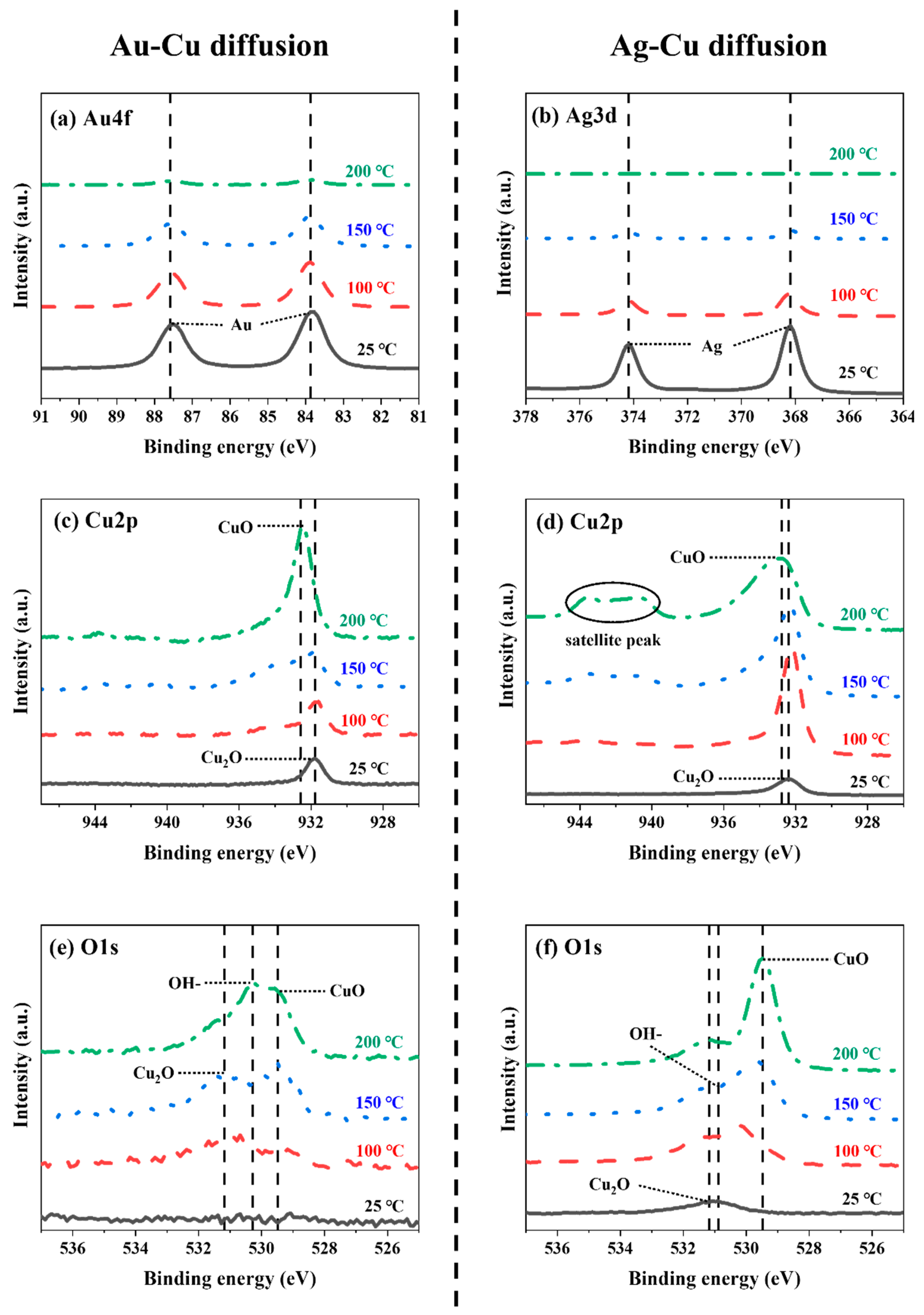
The chemical state and amount of each element (Au, Ag, Cu, and O) were determined by XPS, as shown in
Figure 4, to discern the diffusion characteristics between Ag and Cu, and between Au and Cu. First, for Au and Cu, it was found that the atomic percentage of Au gradually decreases on the surface and the atomic percentage of Cu gradually increases as the temperature increases. In addition, O increases as Cu increases on the surface, likely a phenomenon caused by oxidation due to the increased Cu on the surface as Cu diffuses more actively to Au at higher temperatures. At 25 °C, there is a very small amount of O at the surface compared to the Ag-Cu case. For Ag and Cu, as the temperature increases, the atomic percentage of Ag on the surface gradually decreases, with Ag completely diffused into Cu at 200 °C. The Au and the Ag surfaces both have oxygen because they both have porous structures; in particular, Ag tends to be easily oxidized compared to Au. In
Figure 4e, The O1s peak profile shows that CuO becomes more prominent than Cu
2O as the temperature increases, as Cu is more oxidized and forms a more stable state from Cu
2O to CuO [
19]. Also, under high-temperature heating, the chemisorbed OH- peak appeared to be distinctly high. On the other hand, for Ag, it was observed that Cu
2O changes to CuO as the temperature increases, but unlike the Au case, there is almost no chemisorbed OH- peak, and a strong satellite peak appears around 942 eV, as shown in
Figure 4d. The presence of this satellite peak indicates a similar coexistence of Cu
2+ and Cu
+, although Cu
2+ may be more abundant [
20]. As shown in
Figure 4e,f, oxygen content was observed on the surface before the bonding process in this study due to a porous form of metal nanolayer. To control oxygen permittivity on the bonding surface, a more densely structured metal layer may be required, especially given the use of a nanolayer.
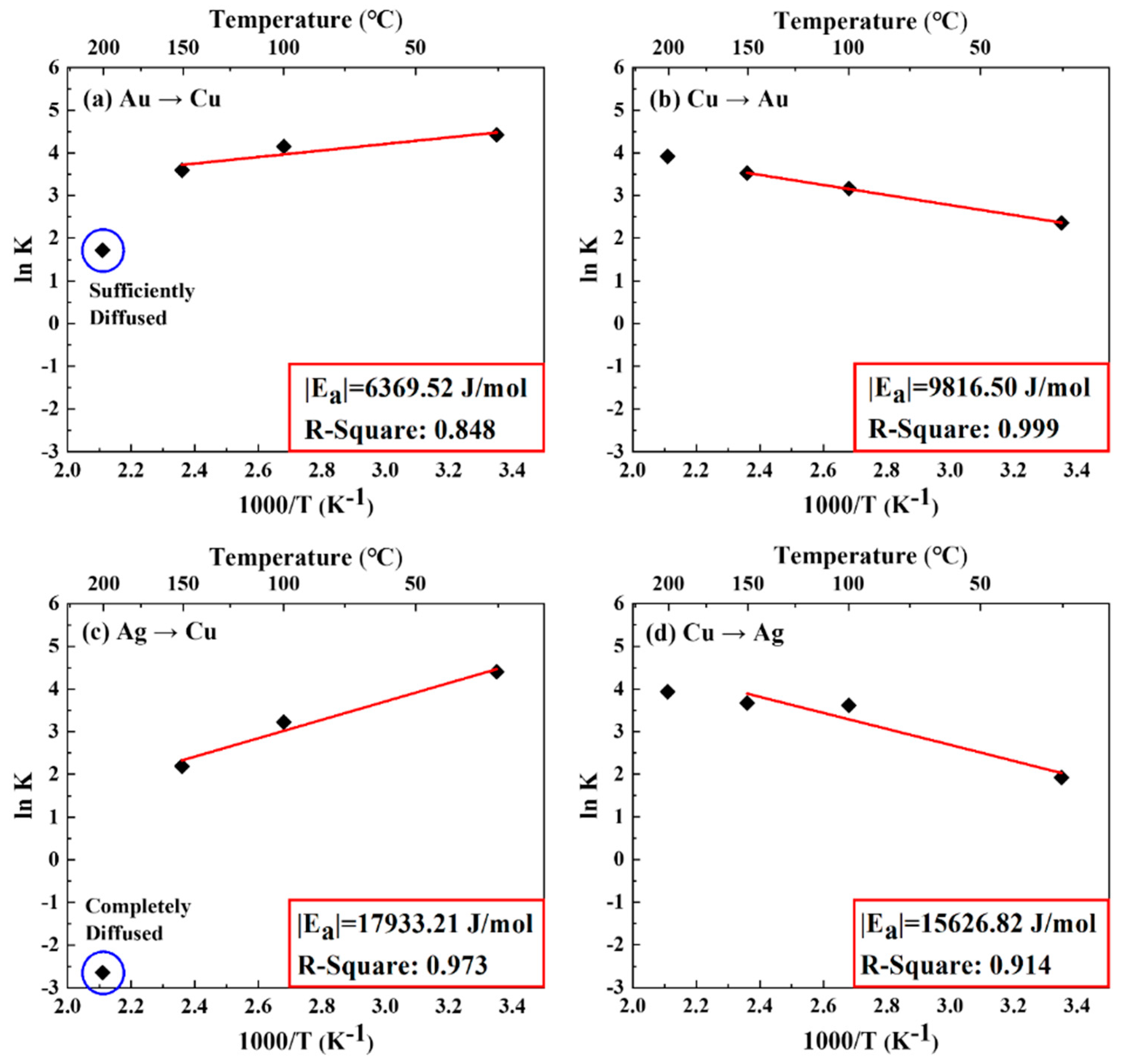
Next, the diffusion activation energy required for diffusion between Au and Cu, Ag, and Cu was estimated using the data obtained through the XPS analysis and with the Arrhenius equation below. In Equation (1) below, K is the amount of each element obtained through the XPS analysis, A is the diffusion constant, E
a is the diffusion activation energy, R is the gas constant (8.314 J⋅K
−1⋅mol
−1), and T is the absolute temperature value.
If natural logarithms are taken on both sides of the above equation, it can be transformed in the following way.
The diffusion activation energy obtained through Equation (2) for Au and Cu was 6369.52 J/mol when Au diffuses to Cu, and 9816.50 J/mol when Cu diffuses to Au, as shown correspondingly in
Figure 5a,b. The lower the diffusion activation energy, the easier the diffusion; hence, according to this result, it is believed that the diffusion of Cu into Au was more difficult than the diffusion of Au into Cu. As shown in
Figure 5c,d, the diffusion activation energy for Ag and Cu was 17,933.21 J/mol when Ag diffuses into Cu and 15,626.82 J/mol when Cu diffuses into Ag, unlike the Au case, showing that the diffusion of Cu into Ag is easier than the diffusion of Ag into Cu. Ag has similar electronegativity toward Cu, while Au has stronger electronegativity toward Cu. Additionally, Ag may be oxidized at the surface, whereas Au does not oxidize at all. Therefore, diffusion from Cu to Ag requires less energy than diffusion from Ag to Cu, while diffusion from Cu to Au requires greater activation energy than diffusion from Au to Cu.
Based on the phase diagrams of Au-Cu [
21] and Ag-Cu [
22], AuCu
3 may exist at 200 °C if an alloy is formed between Au and Cu, but
Figure 4a,c show no evidence of the formation of the AuCu
3 alloy. For Ag-Cu, mostly the α phase, which is the Cu phase, may exist at 200 °C with a minuscule amount of the α phase. In this study, IMC (intermetallic compound) formation was not observed for either Au or Ag due to non-bulk diffusion at high temperatures. The diffusion activation energy value estimated in this study was compared with the diffusion activation energy value of Au and Cu at bulk levels at high temperatures. The activation energy of Au-Cu bulk diffusion at above 700 °C was approximately 178~197 kJ/mol when Au diffuses to Cu and about 169~172 kJ/mol when Cu diffuses to Au [
23,
24]. In addition, the activation energy of Ag-Cu bulk diffusion at temperatures exceeding 700 °C was about 184~198 kJ/mol when Ag diffuses to Cu and about 192 kJ/mol when Cu diffuses to Ag [
23,
24]. Given that diffusion at low temperatures primarily occurs in the form of grain boundary diffusion rather than lattice diffusion, it is unsurprising that the diffusion activation energy observed in this study is lower compared to diffusion at elevated temperatures. Within the scope of this study, distinct diffusion behaviors of Cu on the surface were observed when comparing porous Au and Ag nanolayers with bulk Cu films. In the context of Au-Cu interactions, it was evident that Au exhibited rapid diffusion into Cu, whereas in the Ag-Cu scenario, Cu demonstrated rapid diffusion into Ag.
In general, a high temperature of over 400 °C is required to facilitate Cu bonding, though this can deteriorate the performance of semiconductor devices [
25]. In addition, the bonding temperature of semiconductors varies depending on the product, but low temperatures below 250 °C are increasingly required. Cu bonding using a metal passivation layer can be applied to products either ultra-fine pitch Cu pad structures or larger Cu pad structures with a low Cu volume that does not sufficiently expand at low bonding temperatures. In this study, Cu bonding was evaluated at a temperature of 180 °C, and annealing was carried out at a temperature of 200 °C.
Figure 6 shows the ion beam milling preprocessing conducted for SEM and TEM measurements of the bonding interface.
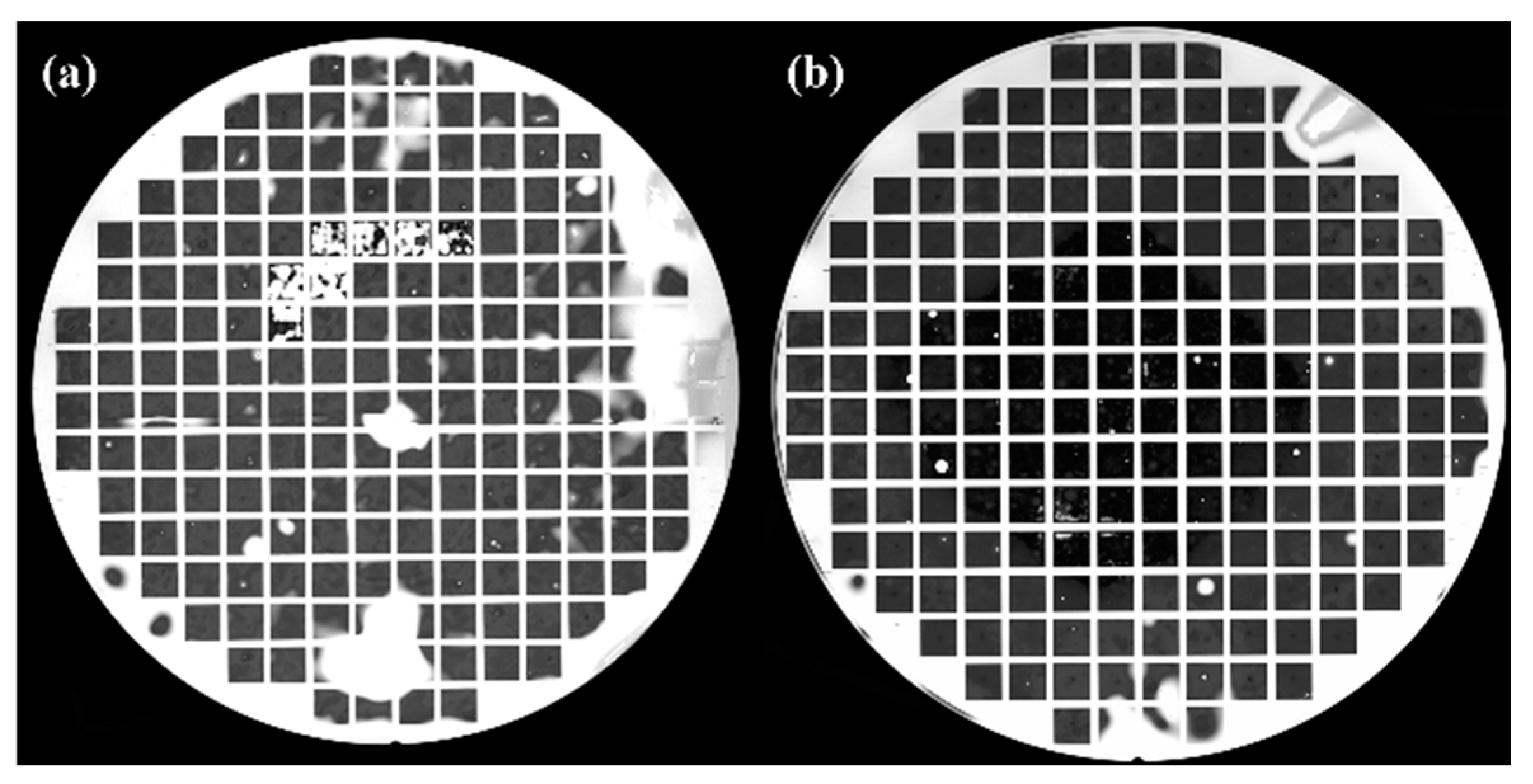
Figure 7 shows the SAT images of the Cu bonding interface with Au and Ag nanolayers.
Figure 8 shows the FE-SEM and TEM results of the Cu bonding interface using an Au nanolayer. In the FE-SEM image shown in
Figure 8a,b, the black area is Cu and oxygen introduced before bonding, and the white line next to the black area is Au. According to the EDS (energy dispersive spectroscopy) line mapping chart in
Figure 8c, a large amount of oxygen was observed at the interface. It is believed that oxygen contamination was already present at the Au and Cu interface before bonding.
Figure 9 shows the FE-SEM and TEM results of the Cu bonding interface using an Ag nanolayer. The use of the Ag nanolayer also led to a pattern very similar to that of the Au nanolayer. However, in contrast to when the Au nanolayer was used, for the Ag nanolayer, oxygen is not observed solely at the Cu region of the interface; instead, it seems to be widely dispersed throughout the bonding interface. This suggests an oxidation process occurring in the Ag nanolayer. Despite the presence of oxygen inflow prior to bonding, it was verified that oxidation of the Ag nanolayer occurred. There is a strong probability that both Ag and AgO diffusion took place during the Ag-Cu interaction. When evaporated Au and Ag diffused inward during the bonding and annealing process, the interface was filled with Cu and O at the surface before bonding.
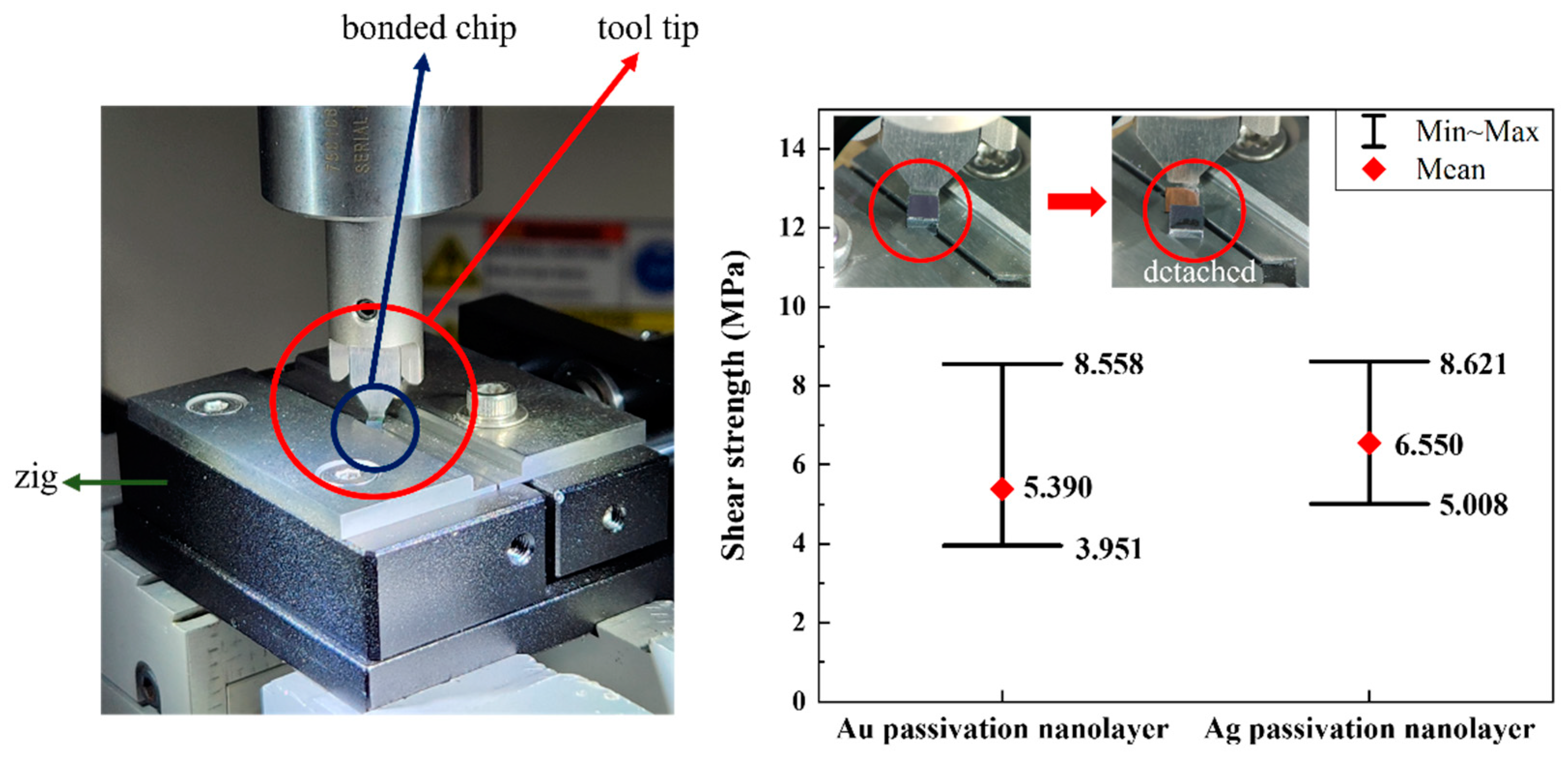
The bonding strength of the bonded specimen was evaluated by shear strength measurements. A specimen of 2 mm × 2 mm in size was used, and the average value was calculated from 20 shear strength measurements. The bottom part of the diced chip was fixed with a zig, and the tip was moved at a speed of 600 µm/s to measure the shear strength when separated by pushing the top part. As shown in
Figure 10, the average shear strength of Cu bonding using an Au and an Ag nanolayer was 5.39 MPa and 6.55 MPa, respectively. For Cu bonding using the Au nanolayers, the average value was slightly lower, and the standard deviation was slightly broader than that of Cu bonding using Ag nanolayers. The relatively low shear strength values in this study can be attributed to two factors: firstly, the low bonding pressure utilized, and secondly, the presence of the non-uniform presence of a metal layer at the bonding interface. To enhance the shear strength of the bonding interface, it is essential to explore a thinner metal passivation layer. Also, the annealing process significantly contributes to improving bonding strength and Cu diffusion. Our current annealing temperature is set at 200 °C, which is the maximum temperature intended for the low-temperature Cu bonding system. Therefore, we may explore the possibility of extending the annealing temperature for further optimization.


