Abstract
Plasma discharges under atmospheric pressure are applicable for modifying the electrical properties of dielectric surfaces. The aim of the plasma discharge treatment of such surfaces is to design a procedure so that its characteristic parameters improve the resulting levels of the breakdown electrical strength Eb when tested under pulsed or alternating electrical voltages. In this research, a set of functional experiments performed by using plasma in samples of two types of materials (thermoset, thermoplastic) were processed and evaluated, and the resulting effect of the magnitude of the breakdown electrical voltage, electrical intensity, and electrical conductivity of the surface were compared. A slit plasma chamber, previously described and parameterized, was employed to treat the surface of the dielectric samples. The surface structure was modified via plasma discharge without precursors, and methodologies were developed to evaluate these modifications with respect to the change in the electrical strength parameters of the insulator surface. Subsequently, the surface strength of the affected and unaffected samples was measured and evaluated as a function of exposure time, and the stability of the modification was assessed. The first methodical test showed that plasma discharge without precursors improved the long-term surface electrical strength of the dielectric surface. The test and its parameters were carried out with respect to feasibility in an industrial environment.
Keywords:
plasma; treatment; dielectric; electrical strength; numerical model; precursor; nanosurface; HV apparatus 1. Introduction to Plasma Generation
In the technology of manufacturing and surface modification, plasma [1] finds use in changing the properties of the upper layers of material surfaces, various mechanical surface adjustment procedures, and altering the properties at the molecular and atomic levels [2,3,4,5]. For such purposes and to achieve physical or chemical changes in the target material surface, the plasma must be generated with a suitable generator [6] under repeatable, pre- defined conditions. To date, plasma-enhanced chemical vapor deposition (PECVD) applications have employed vacuum technologies; presently, however, high-frequency discharge generators to produce plasma under an atmospheric pressure are becoming increasingly more widespread. These technologies, unlike vacuum applications, offer several advantages.
Methods to generate a non-thermal high-frequency plasma discharge have been implemented in diverse industries and exhibit a broad application potential [3,4]. The technology is well developed and has proved interesting especially in thin film deposition [5] or surface modification. The advantage of generating plasma discharges under an atmospheric pressure lies in the possibility of easily forming a local structure with liquid precursors [7]. The electromagnetohydrodynamic properties [1] of generated plasma discharges depend on the design of the electrical generator and the chamber employed to excite the plasma [8,9,10]. The basic chamber arrangement may involve a cold plasma device that utilizes an atmospheric pressure (kINPen), with a central RF electrode and an argon atmosphere [7]. Research has been performed on the COST reference microplasma current in He [8] and the use of an RF plasma pencil to generate plasma [9]. An emerging approach relies on a COST reference microplasma current in He, supported by parallel RF and grounded electrodes [8] and the RF plasma pencil (from the category of the barrier torch discharge, BTD) [9].
The plasma generator, also referred to as the plasma pencil, contains an electrical generator and a high-frequency electrode with an operating frequency of f = 13.56 MHz. When the generator is operating, an atmosphere consisting of argon, nitrogen, and other gases, independent or with admixed precursor gases or substances, flows through the capillary [9]. The qualitative and quantitative electromagnetic discharge parameters are determined by the geometrical arrangement of the chamber, electrodes, shape of the excitation signal of the RF generator, and related parameters [10,11,12].
2. Electrical Surface Strength of Insulators
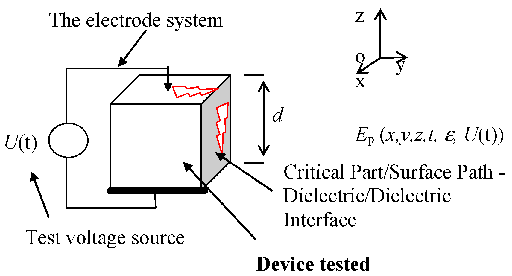
Considering the historical development of the design and manufacture of an HV apparatus [13,14,15] and the design of an electrical apparatus and equipment [16,17,18,19,20], one of the parameters studied is tahe ability of the equipment to withstand the action of an electrical surge. This parameter is tested with both shock waves and a harmonic electric voltage (f = 50 or 60 Hz) for a period of t = 1 s according to the Czech and international standards. In the device or on its surface, during a time period (pulse or t = 1 s), an electrical breakdown can occur through the volume of the insulator and at the insulator interface (dielectric/metal, dielectric/dielectric), Figure 1.

Figure 1.
The principle of the test for the surface electrical strength Ep [V/m] of the proposed device.
Research into the electrical breakdown during testing is relevant to the design of materials, their modification, and when assembling the device/equipment being tested. The solution focuses on achieving a high electrical strength Ep during the testing or operating the device at the insulator interface, delivering a repeatability of the parameters during voltage immunity tests (Figure 1).
Deficiencies in the electrical strength Ep and the repeatability of stress test parameters have thus far been addressed by standard “macroscopic” methods, focusing on:
- (1)
- (2)
- (3)
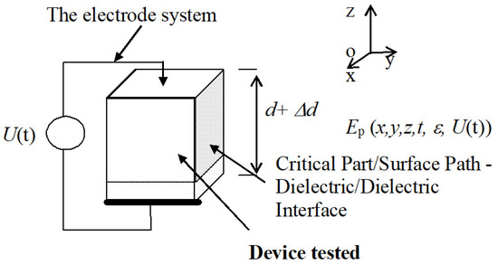
Figure 2.
An approach to improve the surface electrical strength Ep of the designed device by changing the jump distance d.
Figure 2.
An approach to improve the surface electrical strength Ep of the designed device by changing the jump distance d.
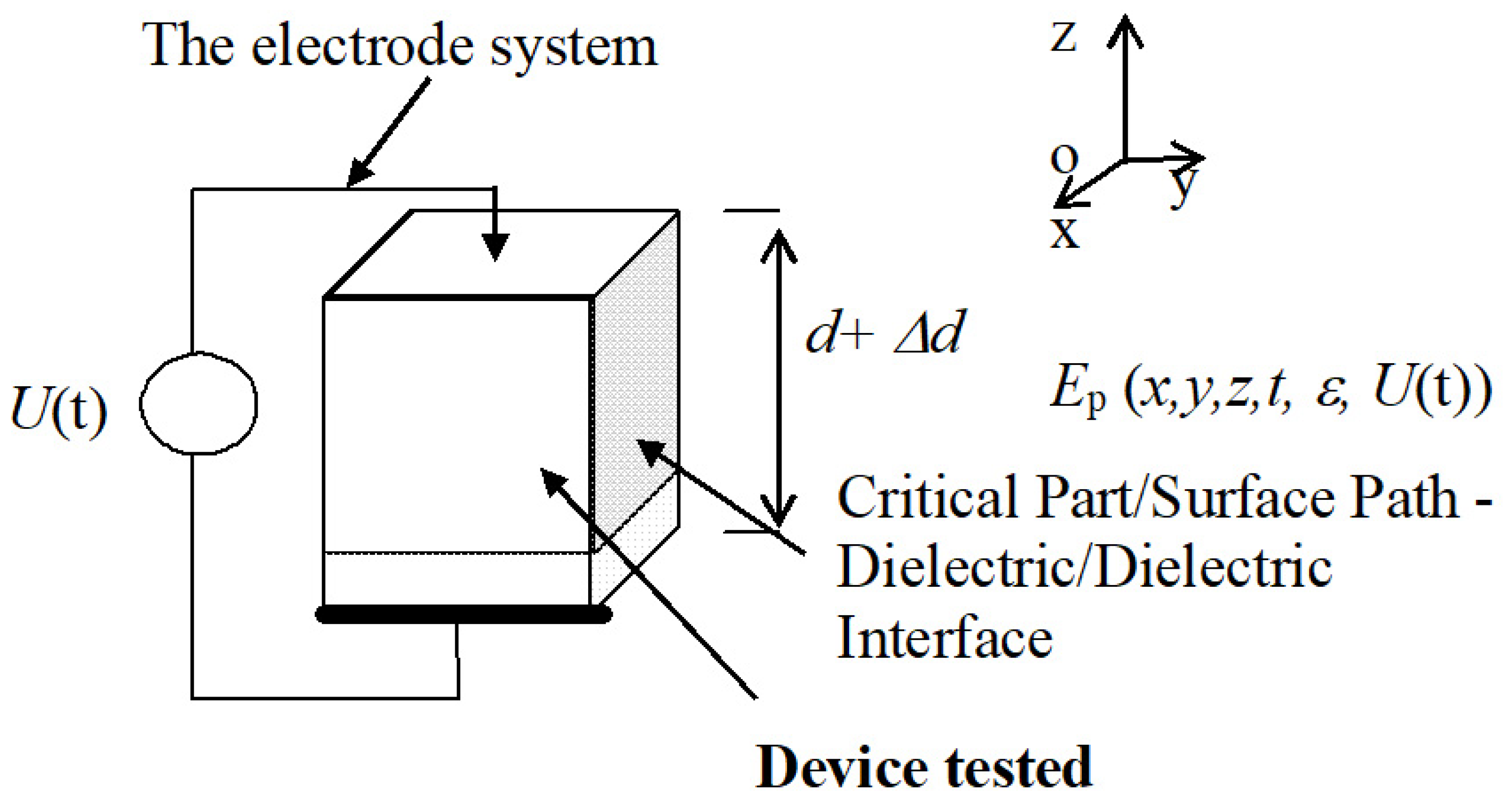
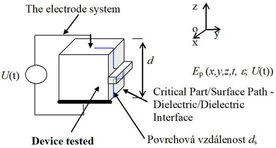
Figure 3.
An approach to improve the surface electrical strength Ep of the designed device via changing the surface distance by an additional element (rib) ds.
Figure 3.
An approach to improve the surface electrical strength Ep of the designed device via changing the surface distance by an additional element (rib) ds.
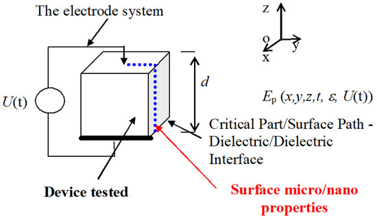
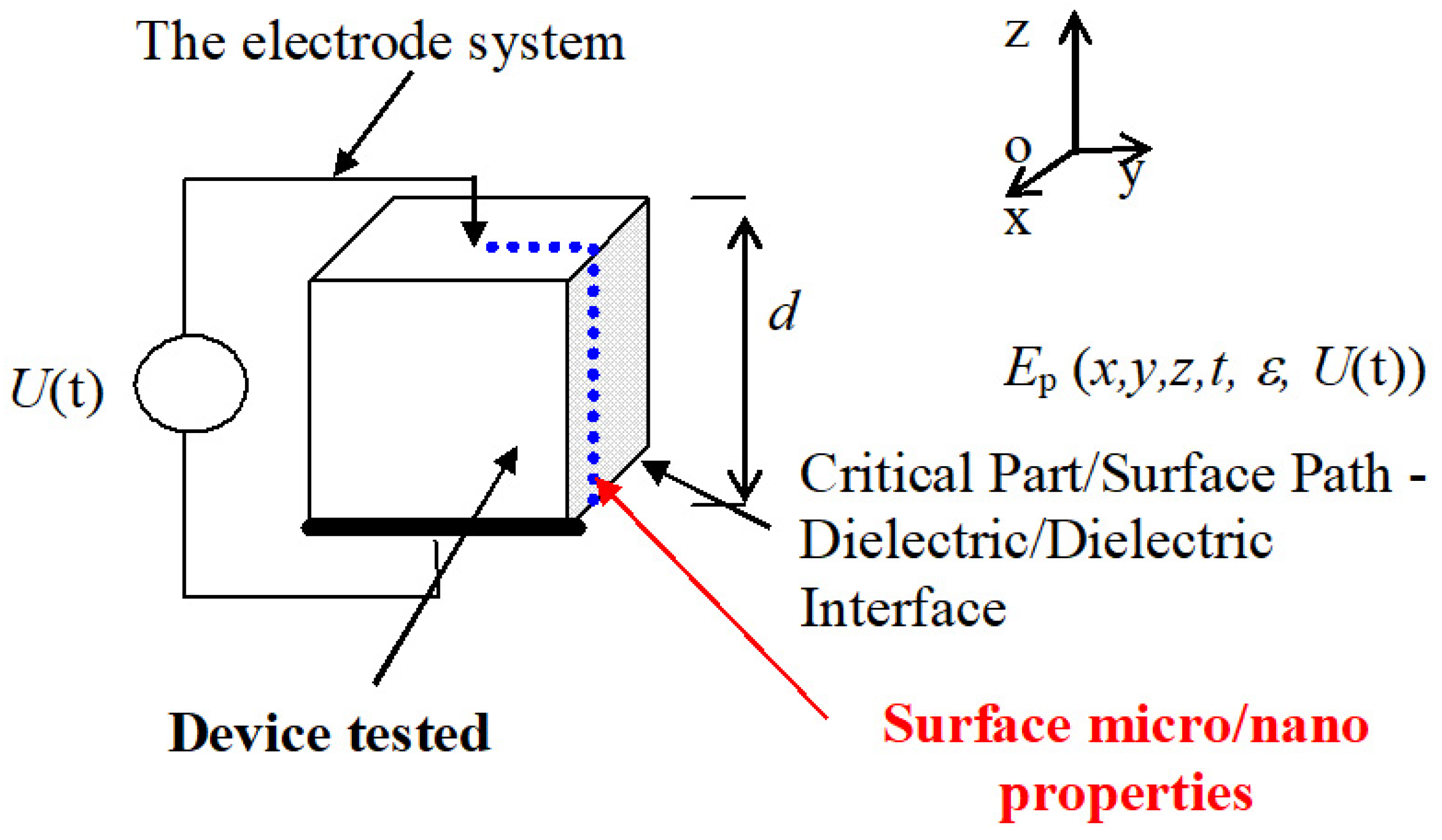
Figure 4.
Increasing the surface electrical strength Ep of the proposed device by changing the micro/nanosurface properties of the insulator.
Figure 4.
Increasing the surface electrical strength Ep of the proposed device by changing the micro/nanosurface properties of the insulator.
The testing of the surface and bulk properties of dielectric materials and designed insulators is described with the standard techniques published in the Czech and international standards. Schematically, however, this could be expressed by setting up a method for measuring the values of the breakdown voltages Ud and breakdown intensities Ep (Figure 5). From the traditional empirical measurement experience [21], it can be argued that the relationship between the bulk and the surface electrical strength is described through an approximate expression as
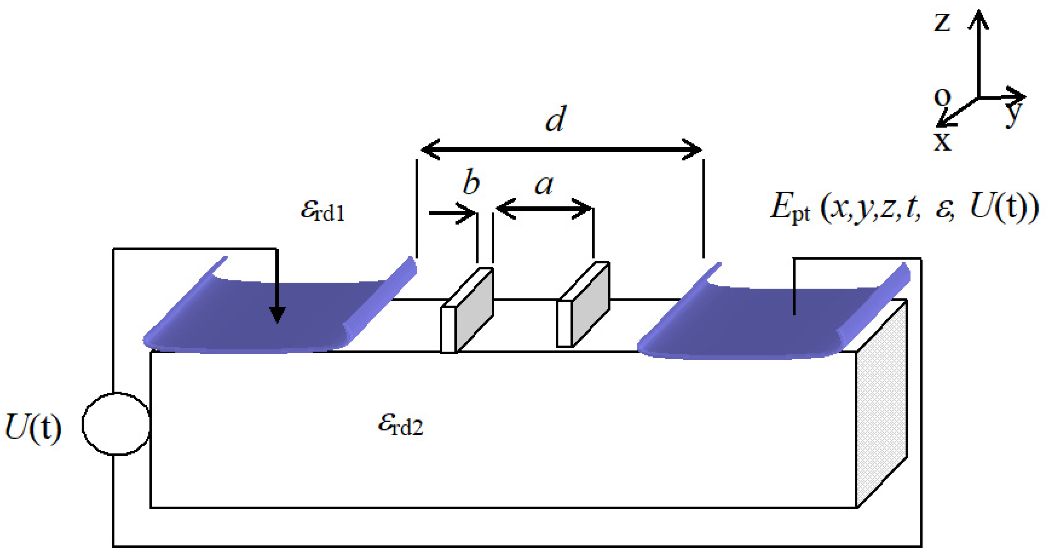
where Epn,ε is the electrical strength in the normal direction characteristic of a material with relative permittivity εr, and Ept,ε denotes the electrical strength in the tangential direction characteristic of a material with relative permittivity εr. The standard treatment of the interface of insulating materials or insulating materials and electrodes of the device under test via method 2 (Figure 3) encounters critical parameters; the essential factor is expressed by the formula
where a, b are the distances and dimensions of the dielectric shaping, respectively according to Figure 6.

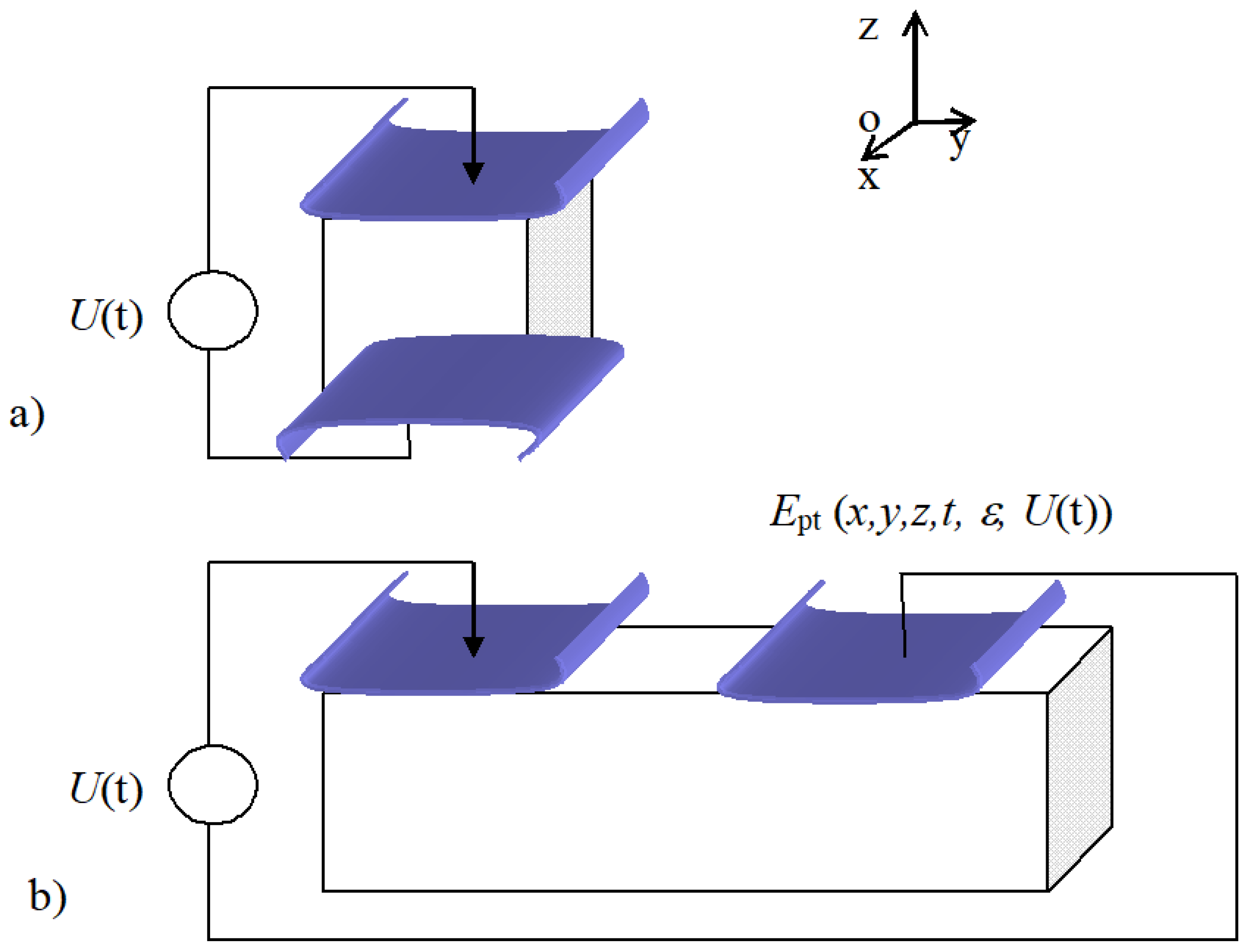
Figure 5.
The principal arrangement and methods for measuring the (a) bulk, and (b) surface electrical strength Ep [V/m].
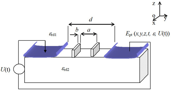
Figure 6.
Methods for adjusting and measuring the surface and bulk electrical strength Ep.
In a system of auxiliary ribs at a finite jump distance d = constant, at a jump voltage Ud (Figure 6), critical Relation (2) is determined by the actual number and geometry of the ribs, which still contribute positively to the increase in the electrical strength Ep of the dielectric–dielectric–electrode interface. If the ratio a/b drops below the critical value of Relation (2), the electrical strength Ep paradoxically decreases, and the opposite resultant effect occurs.
One of the progressive methods for formulating a technical procedure to increase the surface electrical strength Ep in a specific device/apparatus design is applying microscopic (nanoscopic) surface modification of the dielectric–insulator interface. Surface modification techniques, such as sandblasting, facilitate the microscopic roughening of the surface and an increase in the jump distance d. Another progressive method lies in the modification/deposition of a nanosurface on the dielectric to increase the surface electrical strength value Ep. In this context, the effects of the residual electrical charges σ [C/m2] on the surface during impact stress tests are known [22].
3. Current State of the Research and Solutions for the Surface Strength of Insulators
According to well-proven procedures [14,15,16,17,18,19,20], standard devices and HV devices with surface treatment and known materials are designed. The current trends in increasing the surface strength Ep focus mainly on the concept, design, geometric layout of the HV device, and solutions using miniaturization (using microelectronics); one of the related activities then lies in changing the electrical strength of materials, both volumetric and surface ones [23,24,25,26], by choosing the concept and design for the critical part of the device or equipment. The approaches can be characterized and summarized into several categories, as follows:
- (a)
- Insulator surface modification and shaping, both physical and chemical;
- (b)
- Application of layers to increase the electrical strength parameters of the insulator;
- (c)
- Alteration of the nanostructure or the interface surface of the insulator.
Utilizing experiments, the numerical modeling, design, and improvement of the measurement methods of the electrical surface charge σ or the electric field vector E can be carried out.
Further, a more detailed approach to increase insulation properties according to (a) is outlined in [23], for example, where the authors analyze the results of a multiphysics numerical model of a three-pole insulator in a horizontal arrangement, with the operating voltage Un = ± 800 kV GIL (gas-insulated transmission lines), based on this model; the temperature distribution and gas flow inside the GIL insulator are then determined. A similar issue is addressed, with the support of numerical modeling, by the authors of [25] for the DC-GIL system of the ITER project with Un = 1 MV.
Another experimental concept [24] focuses on a set of procedures for evaluating parameters involved in the aging of insulators; the authors of the report discuss methods for evaluating the occurrence of surface discharges, observing space charge generation, and measuring the strength of the dielectric.
In the area of space or surface charge generation and distribution, it has been established that the charge accumulation rate depends on the aging time of the nanostructured resin. The problem of formation, distribution, and lifetime of the surface electric charge σ also depends on the method of combining the dielectric and electrode system. Importantly, the insulator design can cause a disproportionate generation of the local surface electric charge σ [25].
If we examine in greater detail the possibilities in the field of increasing the stress resistance achieved through the deposition of layers, we may emphasize procedures such as minimizing the influence of inhomogeneous or non-isotropic environments [26,27,28,29] on this parameter according to (b); for instance, this option is outlined in paper [26]. To increase the dielectric strength and to reduce the probability of electrical breakdown during voltage tests (due to a surface discharge), the concept of a layered insulator with functional gradient dielectric materials is used.
If we further investigate the results in the field of modifying the nanolayer surface (c) to reduce the discharge activity and to increase the voltage resistance of the insulator, we can consult sources such as [15,30]. Numerical modeling was employed in the hypothesis analysis and verification [15,30]; thus, to configure the measurement process, the system was suitably selected and adjusted to the analysis of a numerical model based on finite element methods [13,30], and the subsequent evaluation of the influence of the micro–nanostructure on the physical parameters of the dielectric.
The dependence of the electrical strength Ep and the micro/nano structure of the dielectric interface was already considered in an article from 1955 [31].
In investigating the mechanism of electrical breakdown in liquids, researchers have sought to measure the electrical strength value Ep that is characteristic of the pure liquid itself; ideally, the goal is to find an Ep value that is free from the influence of any external factors such as electrode composition, the condition of the electrode and dielectric vessel surfaces, and the measurement site configuration. In [31], very reproducible results are provided, allowing the correlation of the electrical strength Ep with the molecular structure of two homologous series of liquid hydrocarbons. This line of research was followed by a more recent project from 2010 [32]; the concept addressed the measurement and evaluation of selected electrical characteristics of nanocomposite materials.
The electrical breakdown voltage value Up and the surface resistance value Rs in PE/SiO2 nanocomposites were evaluated, and a comparison of the results [32] showed that the dispersion of small numbers of electrical nanocharges could improve the observed properties of the synthetic insulator.
Another stream of research on the nanostructure of materials usable as dielectrics was addressed in [33]. Different contents and particle sizes of Cr3C2 in composite materials were tested. The topic of nanocomposite structures was developed in [34]. The electrical strength Ep of nanocomposites containing low-density polyethylene (LDPE) filled with TiO2 nanoparticles was investigated and also evaluated. The surface modification of the TiO2 nanoscale was shown to have a significant impact on the electrical strength during stress tests.
The authors’ research focuses on improving the surface electrical parameters of insulators through surface changes in the order of micrometers or at the atomic and molecular levels. Such modification is not expected to radically increase the breakdown strength with intensity Ep through orders of magnitude; rather, the procedure aims to provide the possibility of an additional technological improvement in a device which has approached the limits of breakdown testing. The modification must have a long-term effect and must not be demanding in terms of technology or funding.
Plasma discharge treatment at an atmospheric pressure nevertheless offers such an additional refinement of the insulator–dielectric surface. As shown above, these technologies are employed in other industrial domains; thus, the authors’ research has centered on generating a suitable plasma discharge by a device usable in relevant branches of the industry [35,36].
Current techniques [37,38] deliver some plasma discharge parameters and evaluations that can be used as procedures and approaches to reduce the surface discharge in a device or apparatus. These options include, above all, the precise adjustment of the electromagnetic-electric field vectors [39,40] and the parameters of the dimensions and nature of the materials, observing the manufacturing technology. Among the experimental projects published to date [21,38,41], a very promising direction lies in creating layered materials at the interface of dielectrics and forming nanomaterial composites with a subsequent increase in the surface strength Ep.
4. Precursors and Surface Treatment
To shape the nanosurfaces of insulator samples, a separate plasma discharge or the insertion of precursors into the gases entering the plasma chamber are applicable; the precursors can be inorganic-based or organic-based [42]. To minimally predict the influence and impact of the plasma discharge on the surface of a dielectric material, it is useful to have a basic numerical model of the precursor and to analyze its electrohydrodynamic properties.
One of the precursors considered is benzene; benzene-based molecules are also usable. Benzene and its derivatives can be geometrically modeled in a simplified way as toroids, or toroids augmented with the probability space of the excursion of the envelope atoms (carbon C and hydrogen H) and the bonds between them [42].
With the produced and utilized samples, the plasma discharge and precursor application was performed. Subsequently, the changes in the electrical properties of such treated surfaces were systematically measured and evaluated for repeatability (type A and B uncertainties) and then compared with untreated samples [43].
The evaluation of the numerical model was based on the results outlined in [42]. The outcomes of the analysis were compared with the experimental evaluations; for example, the frequency spectrum of the benzene model for the Z parameter (impedance parameter) is non-primitive, according to [42]. Such impedances interact with the electromagnetic field of the chamber and its excited frequency characteristic. The mutual interactions and the radiating EMG field change the physico-chemical properties of the precursor and form an output nanosurface on the exposed part of the dielectric surface of the sample.
To predict the formation of new bonds on the dielectric–polymer surface via precursors, we need to know the precursors’ electromagnetic properties. Substances based on benzene molecules embody the elementary types of precursors used. When these interact with the plasma discharge, new bonds are formed on the surface to be treated; the treated surface then changes its parameters. For our purposes, the surface strength was monitored. Knowing the results of the analysis of the models allowed us to design an effective measurement method for diagnosing the discharge and the condition of the treated surface.
5. Methods of Adjusting the Electrical Strength of Dielectrics: Surface Strength
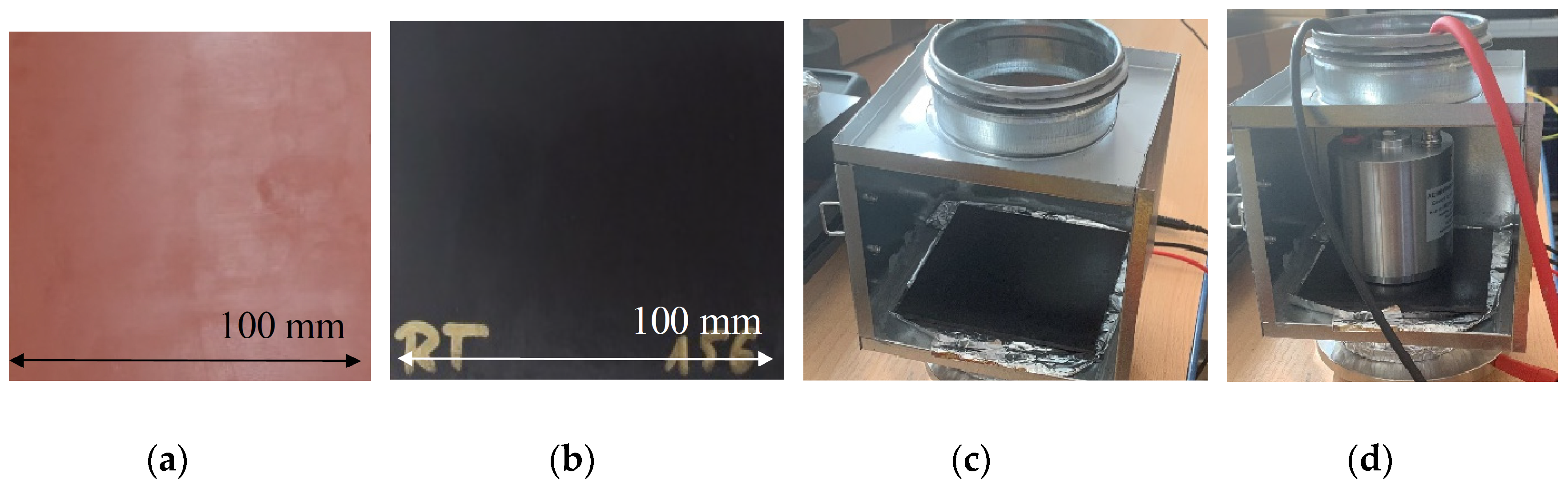
In order to achieve the desired surface treatment and to change the parameters, it appears convenient to use the plasma technique under atmospheric conditions, thus modifying not only the mechanical and structural but also the electrical properties of the sample. Such a state of the dielectric and its surface in the structure of the insulator is suitable for changing the surface strength parameters, both with and without the use of precursors. As a basis for testing and verifying the plasma modification of the dielectric surface, we created samples of dielectric insulating materials: an epoxy-based thermoset and a PE thermoplastic polymer, Figure 7.

Figure 7.
Samples of dielectric materials for HV insulators and insulating parts: (a) epoxy base-termoset type, (b) PE-thermoplastic base, (c) chamber for surface strength measurement, (d) chamber and sample with a probe for surface strength measurement.
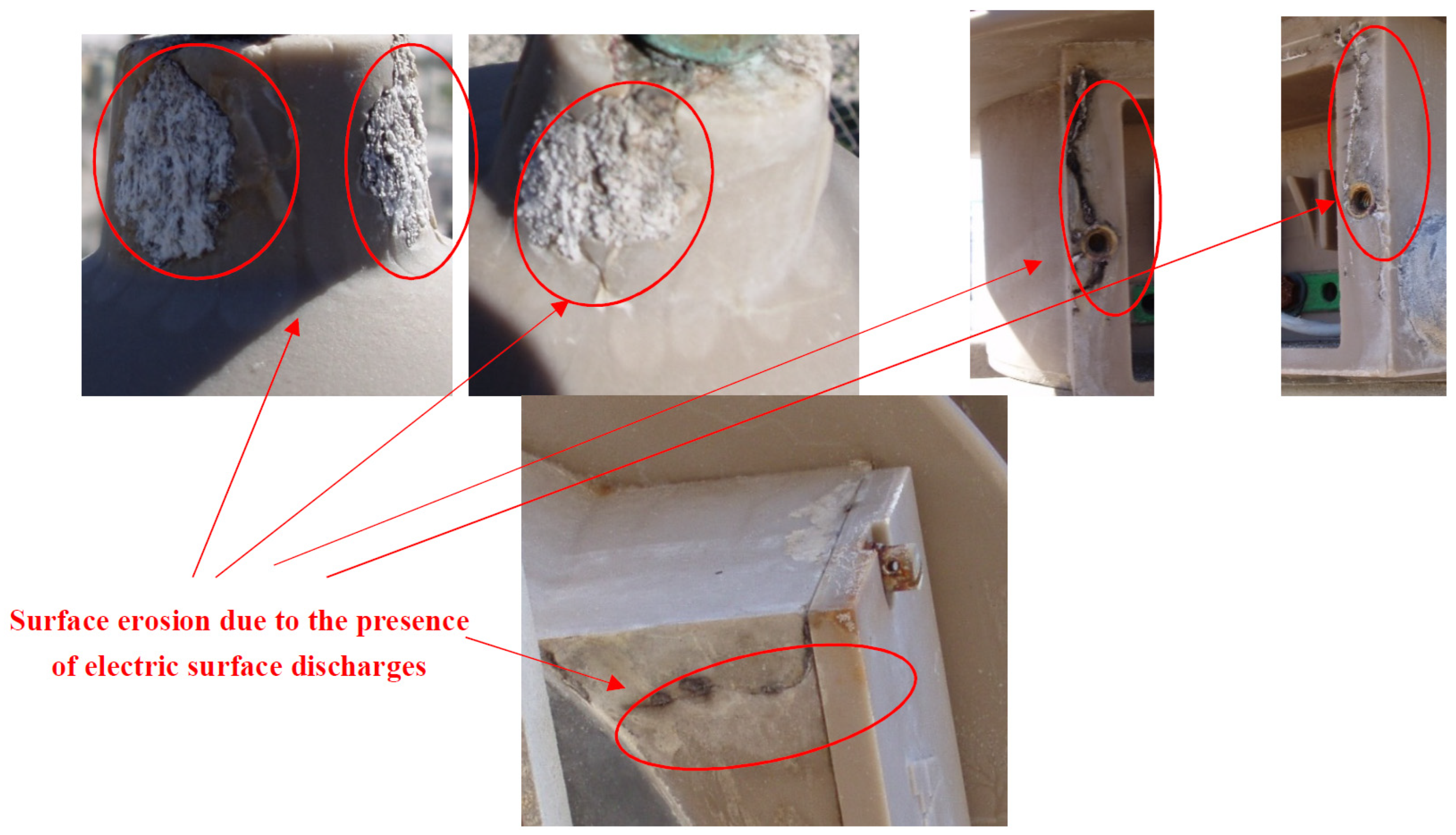
The surface electrical strength Ep and its management in insulators, together with modifications of the geometrical or surface design of the equipment, are important for outdoor and indoor installations of apparatuses and equipment for the LV, HV, and UHV voltage classes. This requirement is determined by the durability or long-term safety and safe operation of the designed/manufactured equipment, identification, detection, evaluation of initial discharges and discharge activity, and use of surface modification technologies [1,44]. An example of the impact of long-term exposure to increased electrical intensity of the surface discharge Ep on the condition and operation of the equipment is shown in Figure 8; in this context, significant factors include not only the quality of the equipment (aging) in terms of safe operation, parameters and changes/impacts on the insulator surface, but also the design and construction of the equipment itself with respect to minimizing the conditions for generating surface electric field intensity Et [43].
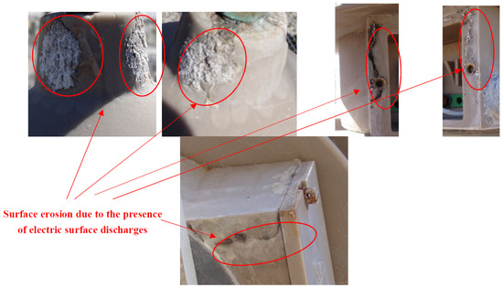
Figure 8.
Effect of increased electric field strength on the HV insulator surface in the aging process of the insulating material.
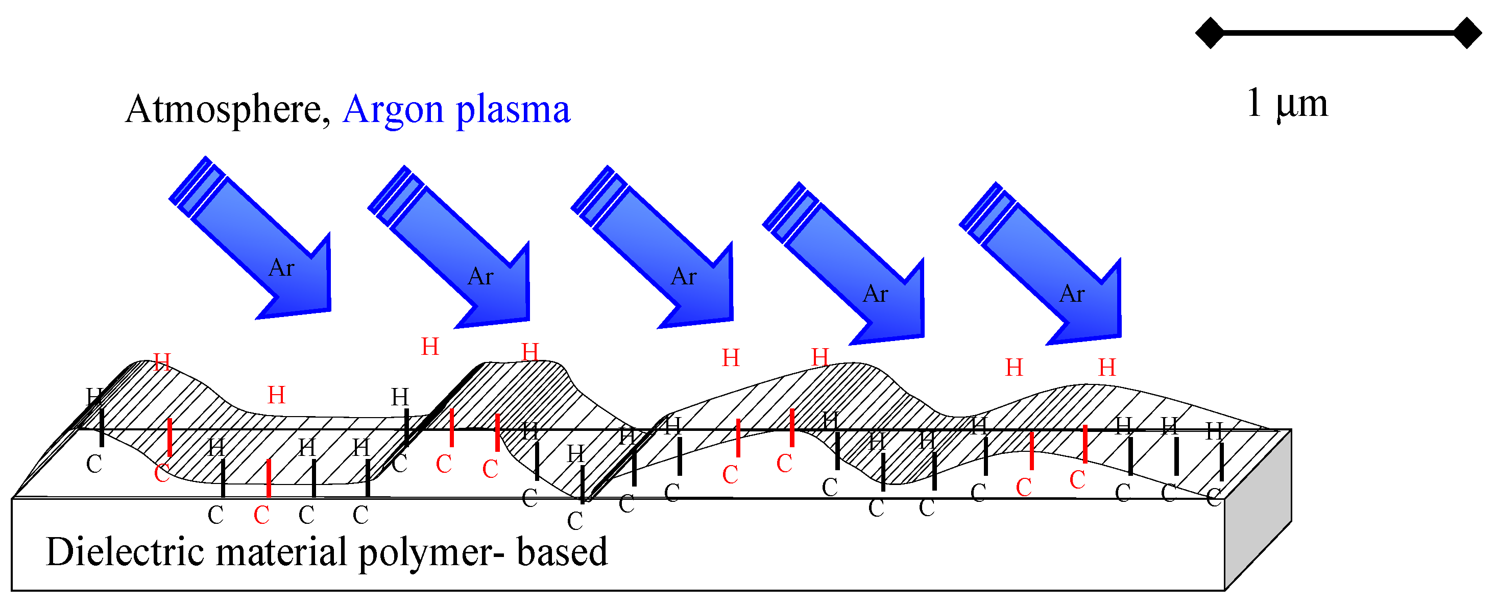
From previous research [36,37,44] on the properties of precursors of organic origin [36,42], the basic experiments with the effect of the plasma atmospheric discharge treatment [4,5,6,7] on the surface of the dielectric, together with the evaluation of changes in the relevant parameters, have moved to the application level (GA 20-14105S) [37,43]. In a recent article by Polášková et al. [37], the scientifically proven mechanism of surface changes through the action of plasma generated by a slit jet is approached. Interestingly, a part of the report is centered on elucidating the physico-chemical processes during the action of plasma at the interface of the dielectric material in a free atmosphere. The basic principle lies in the creation of electromagnetic conditions at the dielectric/air surface interface, such that the strong action of the electromagnetic field and temperature changes the arrangement and molecular composition of the thermoset and thermoplastic polymers; see Figure 9 and Figure 10. The result of the measurement of the incident plasma spectrum at the dielectric interface is exposed in Figure 11. The design and tests of the chamber have previously been published [9,10,12,36,44]. These chambers can be set up, and they parametrically affect the surface of the samples with plasma in a repeatable manner, monitoring and documenting the impact of plasma matter on the surface and the formation of artifacts (Figure 12 and Figure 13). These changes and new formations vary both from the point of direct action of the atmospheric plasma discharge (Figure 14) and according to the chosen setting of the plasma-generating chamber mode and frequency spectrum (for example, the spectrum presented in Figure 11). A more in-depth qualitative evaluation and approximation of the process to influence the polymer surface via atmospheric plasma discharges was proposed in [45,46]. Such treatment procedures, if performed properly, induce changes not only on the surface of the dielectric in the microscopic region (Figure 12 and Figure 13) but also at the level of the polymer molecules and atoms [45] (Figure 15). The surface is altered in its molecular structure and the newly formed chains cause a macroscopic change in the surface of the material (Figure 15). The expected bonds are those that are potentially able to bind an electric charge, and this results in a macroscopic increase in the interfacial strength of the modified surface, Ep. This hypothesis has already been investigated and tested in other areas of electrochemistry [45,46]. Therefore, the authors attempted to verify it by measurements, whether a change in surface strength properties could also be expected. The authors worked with the hypothesis of an increase in the capture of free electric charges moving along the surface at threshold parameters before the electric discharge effect (Figure 15). These electric charges (negative) can bind to the free hydrogen bonds of the bridges and do not complete the electrode–electrode path of the test electrode system. In its effect, such a mechanism increases the electrical strength, which has been quantitatively tested and demonstrated. These effects then deliver the result schematically outlined in Figure 4. Thus, changes in the parameters can be expected when testing the surface strength of the dielectric.
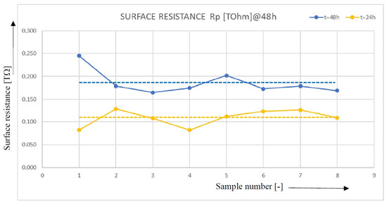
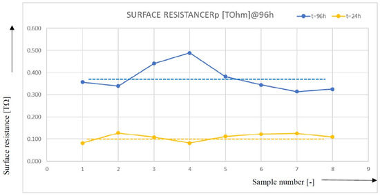
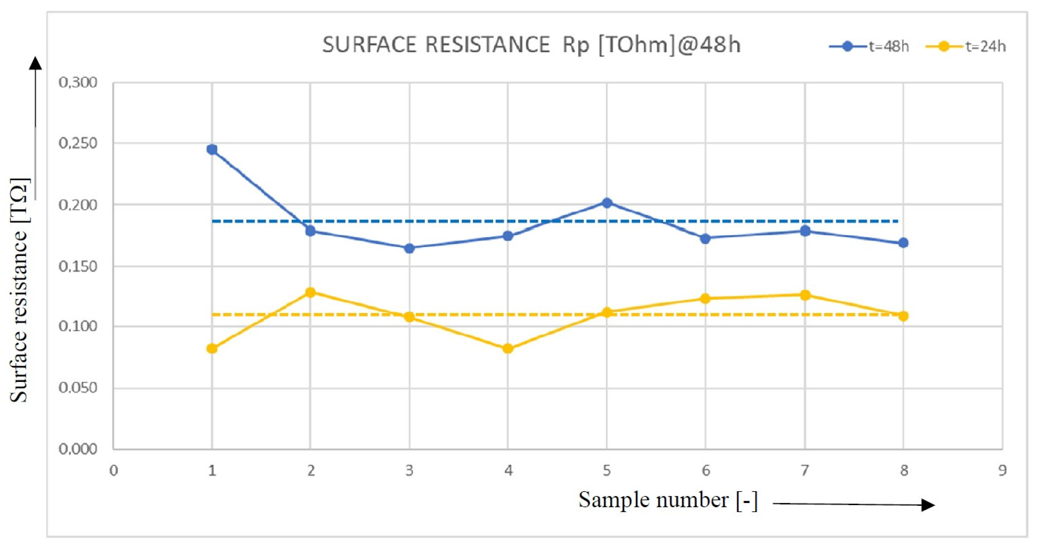
Figure 9.
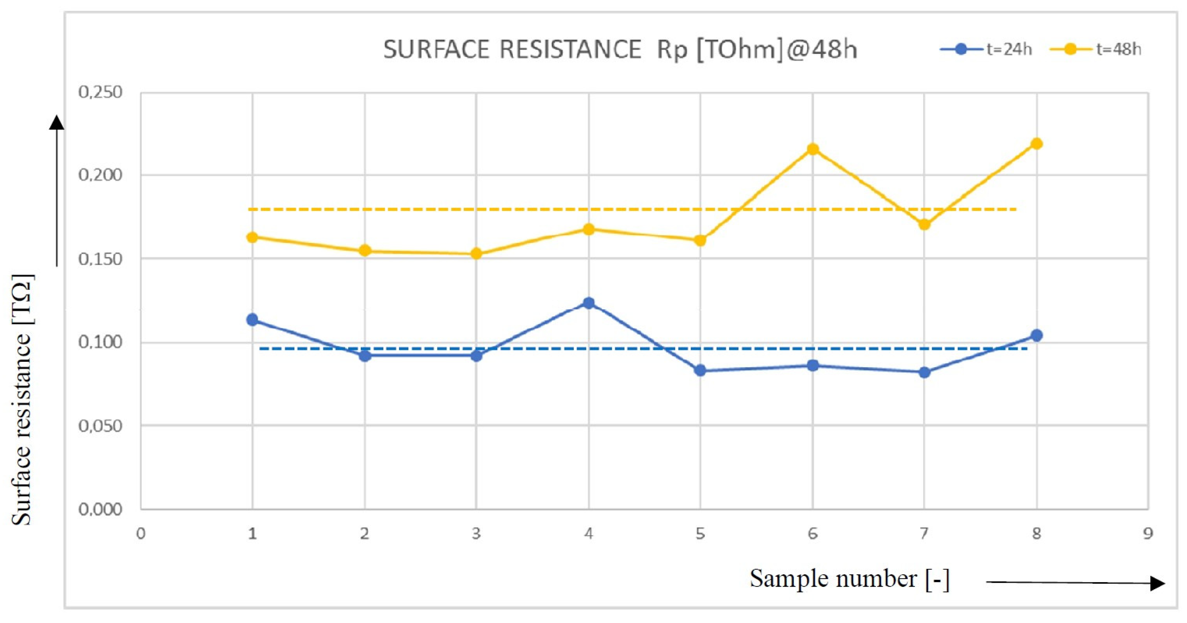
The evaluation of the time dependence of the change in surface treatment on the value of the surface resistance Rp for a thermoset sample (the dashed value is an expression of the average value of the quantity), second series.
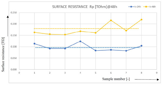
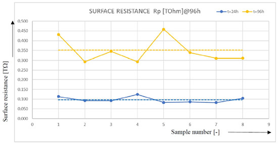
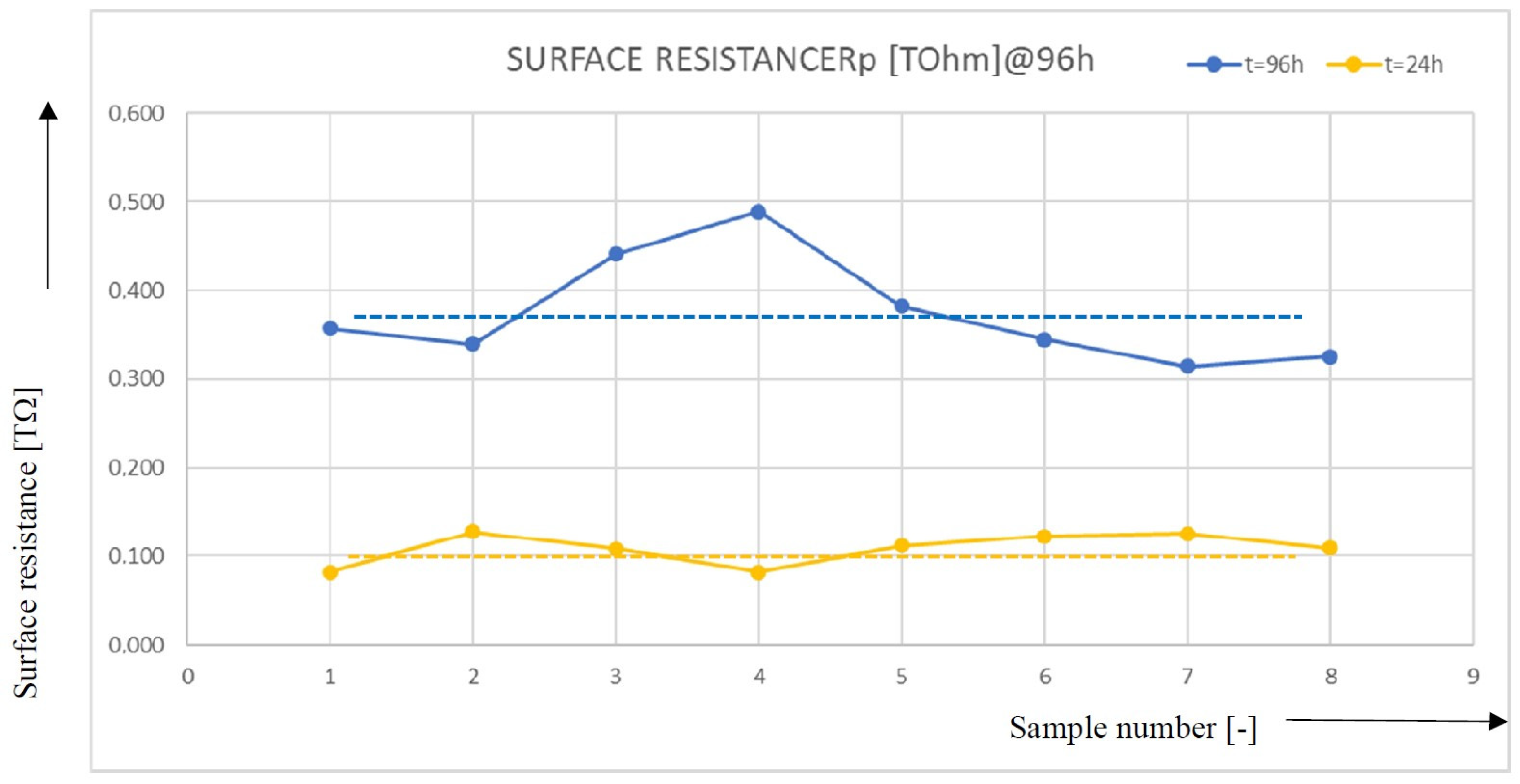
Figure 10.
Evaluation of the time dependence of the change in surface treatment on the value of the surface resistance Rp for a thermoplastic sample (the dashed value is an expression of the average value of the quantity), second series.

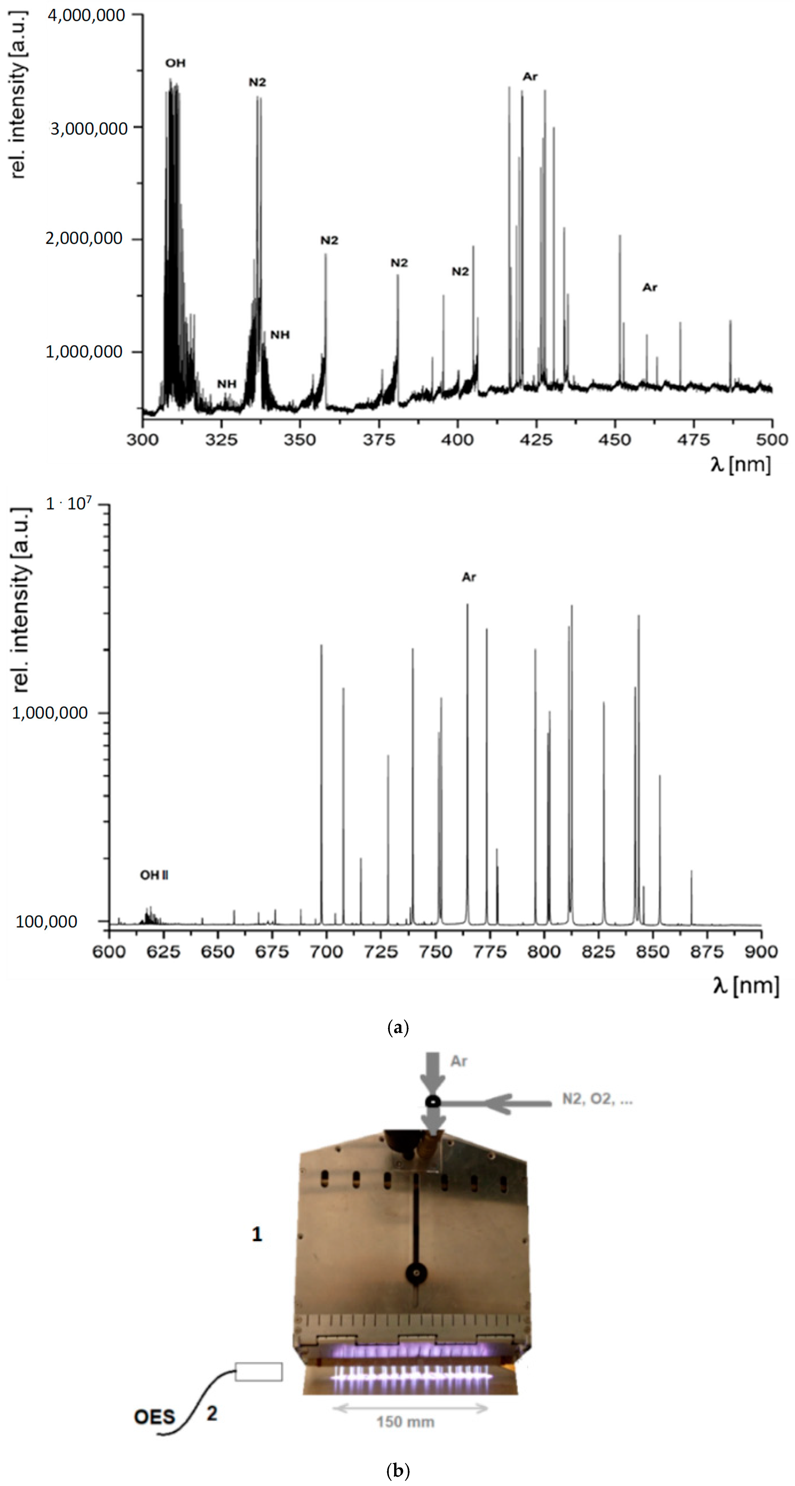
Figure 11.
Evaluation and overview of the optical emission spectrum of PSJ type A plasma (a) for Pout = 500 W, flow Ar w = 5 L/min. (b) Arrangement of the plasma diagnostics; experiment-1—plasma nozzle, 2—optical probe.
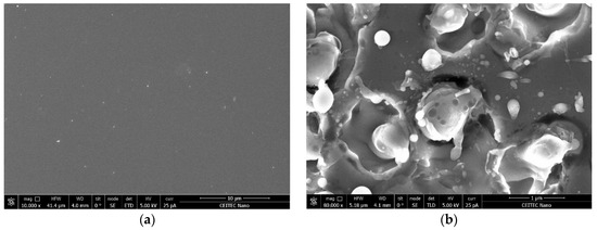

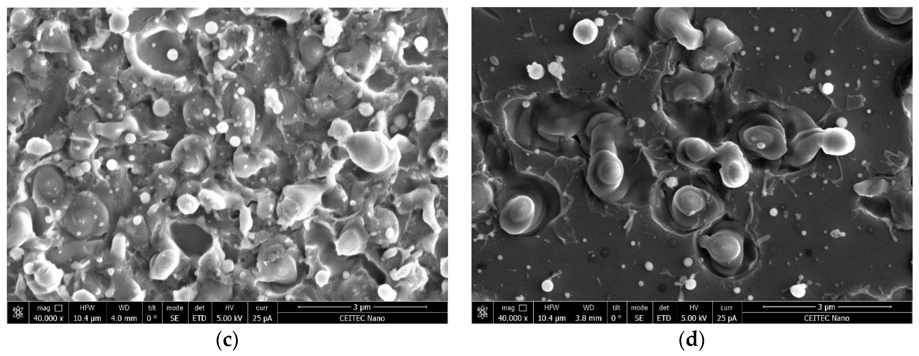
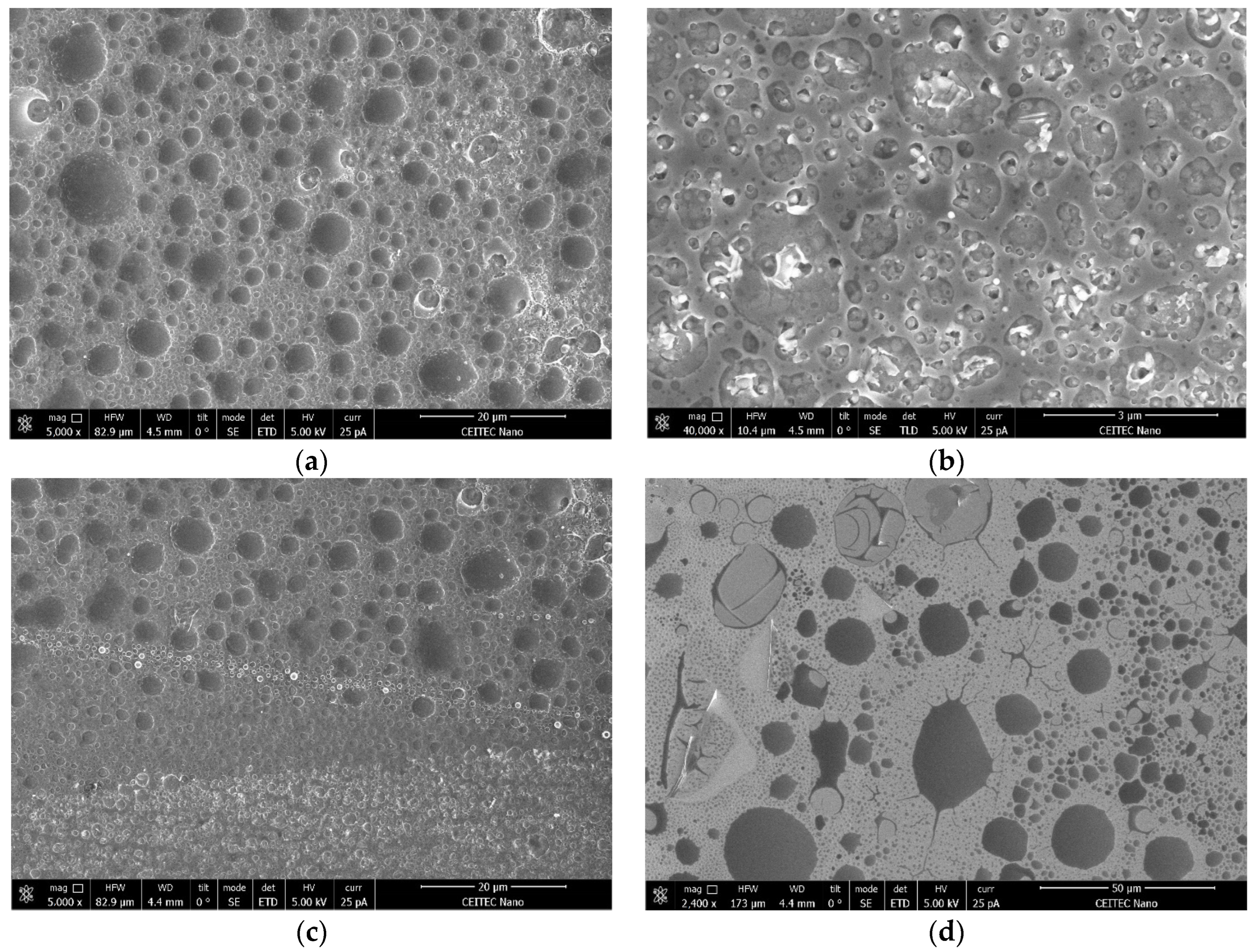
Figure 12.
SEM of the dielectric sample surface after plasma treatment by adjusting the selected spectrum A: (a) sample region outside the plasma effect, (b) central region of the plasma effect, (c) transition region, (d) edge of the plasma effect.

Figure 13.
SEM of the surface of the dielectric sample after plasma treatment by adjusting the selected spectrum B: (a) central region of plasma action, (b) different type of structure in the central region of plasma action, (c) transition region between structures (a,b), (d) edge of plasma action.
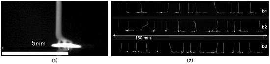
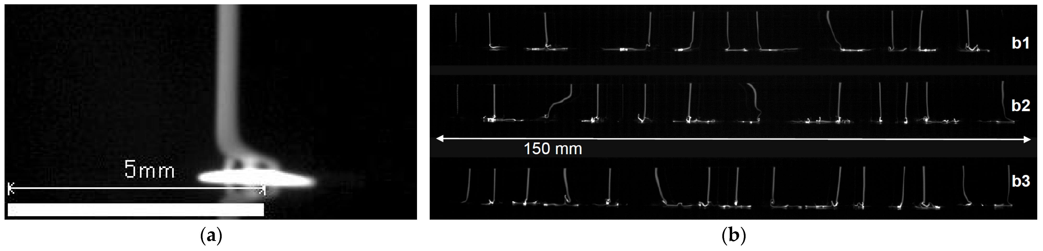
Figure 14.
Discharge behavior and distribution on the dielectric surface captured by the high-speed camera: (a) one column of discharge, (b) a series of PSJ discharges from the plasma nozzle mouth and on the sample surface with frequency spectra (40,000 fps, shutter speed 5 µs), (b1) power 500 W, flow rate Ar w = 4 m3/h, (b2) power 500 W, flow rate Ar w = 6 m3/h, (b3) power 600 W, flow rate Ar w = 6 m3/h.
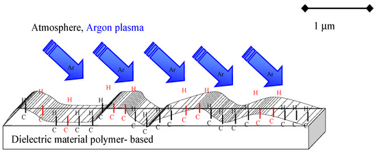
Figure 15.
Schematic arrangement of microscopic and atomic changes in polymer dielectric surface after PSJ plasma discharge treatment, the newly formed chains of bonded atoms.
In this section, the methodology of applying an atmospheric plasma discharge on the surface of a dielectric sample is presented (Figure 7a,b). The process utilized a generator with the output power Pout = 10–1000 W, Uout = 300–600 V, a periodic signal, and the first harmonic f1 = 13.56 MHz (Figure 14). According to the previously performed experiments (from 1996 until now [4,7,9,10,35,36,45,46]), the parameters (Figure 11) of the electric power of the exciting slot nozzle of the plasma discharge in gases, for example, were obtained based on experiments with Ar, N2, etc., to effectively influence the surface. An example of the impact of changes in the plasma surface is shown in the images of the surface in Figure 12 under different settings of the discharge parameters. Furthermore, the effective state of the discharge on the surface of the dielectric is indicated in Figure 14, with the generator parameters set. Other settings can be applied, but they either achieve the necessary efficiency, significantly change the surface, or the permanence of the change in surface properties is insufficient. Thus, in the laboratory, air pressure was maintained in the range of p = 101.30–102.2 kPa, under daylight (wavelength of 440–780 nm, temperature distribution for white light of 4800–5100 nm), with a luminous flux of 1500 lm, and humidity of 45–55%. These experimental condition data are quite justified for laboratory research. However, for the planned possible deployment of this technology in an industrial application, their achievability in a factory environment must be considered and accessibility taken into account. Therefore, no major precautions were taken in terms of setting up and maintaining very harsh laboratory conditions. The repeatability of the effective plasma action on the sample was ensured by a conveyor belt with a set feed rate of v = 22 mm/s. The samples and their surfaces were subjected to plasma discharge twice on the same surface to ensure good homogeneity of action on the surface. After the first exposure, the samples were rotated 90° and treated again with plasma at the same height of the PSJ mouth above the sample surface equal to h = 10 mm.
Because of the targeted involvement of the technology in the production of HV devices, the authors also decided not to modify and clean the surface of the samples before plasma application. In the anticipated production use, these measures (cleaning of the device surface, air pressure, humidity, lighting conditions, etc.) would be unrealistic to follow repeatedly in several respects. However, test results indicated that measurable changes in electrical surface strength parameters can be expected.
5.1. Detailed Description of the Plasma Surface Treatment
The plasma was generated through a setup including a power frequency generator and a plasma chamber producing a plasma slit beam (PSJ). The effective area of the plasma beam amounted to 150 mm. The plasma was generated in an argon atmosphere conducted into the plasma nozzle at a flow rate of w = 4 m3/h. The high-frequency power generator to produce the PSJ had an operating frequency of the first harmonic at f1 = 13.56 MHz, and the output was regulated to a power of up to Pout = 600 W. In the first series of experiments for the surface modification of polymer dielectric samples (six samples, two controls) the power was set to Pout = 500 W. The repeatability of the plasma impact on the sample was ensured by a belt conveyor having a set feed rate. The samples and their surfaces were exposed to the plasma discharge twice in order to ensure good homogeneity of the influence on the surface (the feed rate was set to vd = 22 mm/s, and the height of the PSJ mouth above the sample surface equaled h = 10 mm). The selected sample size to demonstrate the effect was chosen to be a × b = 100 × 100 mm; such a parameter facilitated easy handling and the capture of the homogeneity characteristics of the plasma exposure. All dielectric samples of the second series, both the thermoplastic and the thermoset types, were exposed in this way in a time sequence. In each of the two subsets, a total of N = 8 samples were exposed, while 2 samples were left unexposed to allow a comparison of the measured parameters. The distance to the plasma nozzle mouth from the sample surface was micrometrically set to d = 10.0 mm. For the measurement of the surface parameters (Figure 7) with the probe (Figure 7d), and the required measurement purposes, the standard recommended “suitable” electrode and dielectric arrangement concept (IEC 61340-5-1- [47], ESD STM 11.11-2001- [48], ASTM Standard D 257-99- [49]) (Figure 7d) was chosen. The test probe and specimens were chosen to accommodate a minimal deformation of the field lines due to the geometry of the surrounding environment and to satisfy the accuracy of the testing. The configuration could then be considered as a homogeneous and defined environment.
5.2. Surface Treatment and Measuring Methodologies
The test methodology and relevant parameters were verified as follows:
- In the first step, the proposed methodology was employed for measuring six samples, two without a surface treatment and four with the surface exposed, by an atmospheric plasma discharge. The treatment was performed on samples of both types of material, namely, epoxy resin-based and thermoplastics-based materials.
- After verifying the parameters and repeatability of the discharge exposure, the procedure was conducted again, this time on 10 samples of each category.
- Before and after exposing the sample surface to a plasma discharge, we measured and evaluated the residual surface electric charge σ [C/m2], surface resistance Rp [Ω], and electric current passing through the sample Is [μA].
- The time dependence of the stability of the parameters Rp and Is was tested, and the measurement according to point 2 was repeated at pre-defined time intervals T, namely, 24 h, 48 h, 72 h, and from 120 h to 144 h after exposure to the plasma discharge.
- The post-exposure samples were transported in a container with a defined material and surface conductivity, pre-determined dimensions, and material structure/composition. The surface electric charge was measured and adjusted to ensure minimum surface charging of the exposed sample during storage and transport to the measurement laboratory.
Regarding the surface parameters of the samples after treatment, these were measured according to the above-mentioned procedure in the following manner:
- Measuring system calibration: device, probe, environment, unexposed sample.
- Measurement and evaluation of the resistance Rc using a CA-6543 device, Chauvin Arnoux, France.
- Simultaneous measurement of the electric current Is using a Kethley probe EA10000, Keythley, Tectronix, USA.
- Evaluation of the resistance Rv, electric surface charge density σ, and electric intensity E in exposed and non-exposed samples.
- The entire procedure 1–4 was repeated for the interval T, namely, 24 h, 48 h, 72 h and from 120 h to 144 h.
- Evaluation of the measured data and graphic recording.
The treatment methodology is shown in Figure 16.
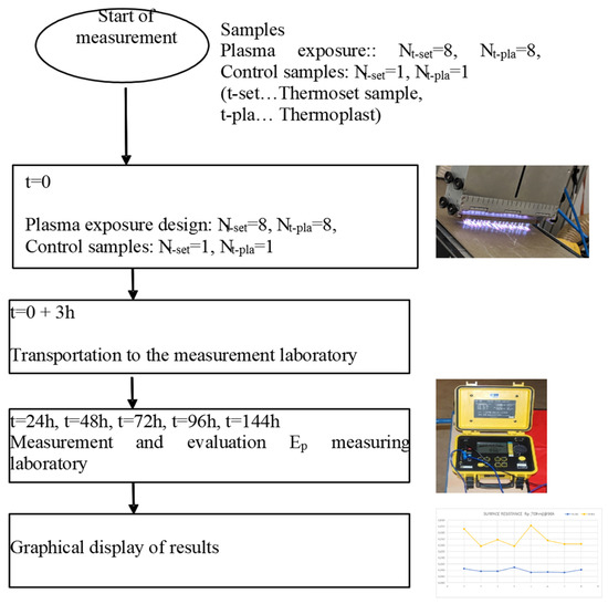
Figure 16.
Schematic of the measurement process and verification of the parameters of the tested dielectric samples.
6. Experimental Evaluation, Results, and Discussion
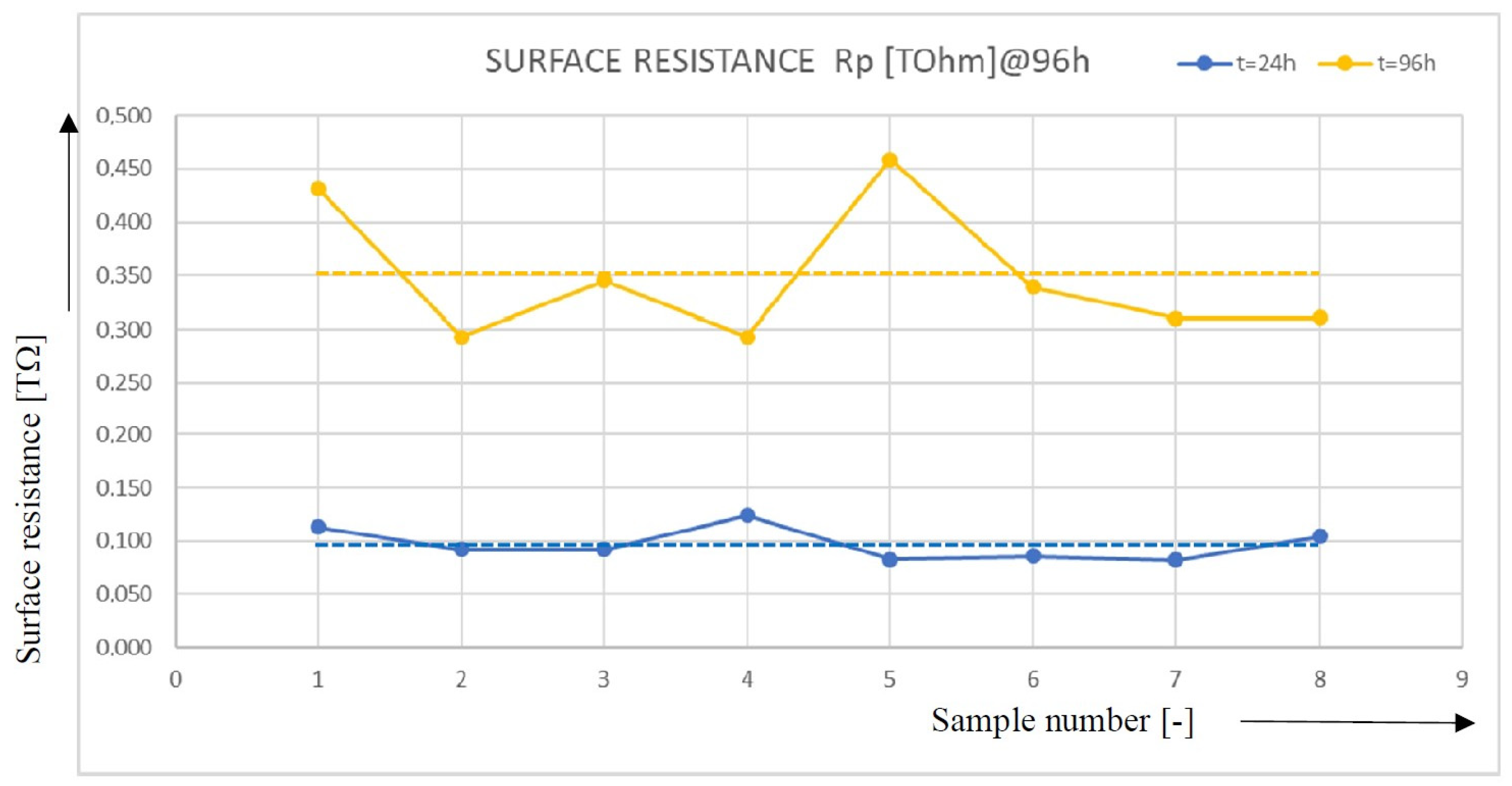
Based on the described measurement methodology [35], the evaluation of the time dependence of the monitored treatment parameters and the verification of the influence of the surface conductivity/resistance of the insulator sample were graphically represented. The designing and testing of the PSJ were described in [35]. For the given purpose, a generator [36] with the output power of Pout = 10–1000 W, Uout = 300–600 V, a periodic signal, and a first harmonic of f1 = 13.56 MHz was used. The graphical patterns of the tests of changes in the surface resistance of the insulator as a function of time (from the exposure time without a precursor) are shown in Figure 9 and Figure 10. The surface resistance of the untreated samples of the second series of materials was Rp,tset = 0.082 TΩ, and Rp,tplast = 0.092 TΩ. According to the previously performed experiments (from 1996 until now [4,7,9,10,35,36,45,46]), the parameters (Figure 11) of the electric power of the exciting slot nozzle of the plasma discharge in gases, for example, were obtained based on experiments with Ar, N2, etc. to effectively influence the surface. An example of the impact of changes in the plasma surface is shown in the images of the surface in Figure 12 under different settings of the discharge parameters. Furthermore, the effective state of the discharge on the surface of the dielectric is indicated in Figure 14, with the generator parameters set. Other settings can be applied, but they either achieve the necessary efficiency, significantly change the surface, or the permanence of the change in surface properties is insufficient.
When setting different parameters of the discharge, for example, the electric power Pout for f = 13.56 MHz, with gas flows such as argon, nitrogen, air-argon, very different changes in the dielectric surfaces can be achieved. As an integral part of the research on the influence of the parameters of dielectric surfaces, the evaluation of their states during the parametric setting of the discharge is necessary. This part of the research is not the subject of this communication, but an example of surface changes on the dielectric material is given in Figure 12 and Figure 13. The images at the corresponding magnification scales are shown there. The structure of the surface testifies to the possible hypothesis of the formation of free bonds on the surface, as shown in Figure 15, where broken hydrogen bonds are indicated in red, which then remain at the surface, and the free hydrogen atom H is removed during the plasma discharge.
In designing the test, it was known from previous work [35,41,42,44] that plasma-treated surfaces changed, their nanochemical composition changed, but at the same time, a remanent electrical charge remained on the surface. This in turn may affect the resulting effect of measuring the long-term change in the electrical strength of the surface. Therefore, it was decided in the measurement methodology to repeat the measurements after some time intervals (Figure 16).
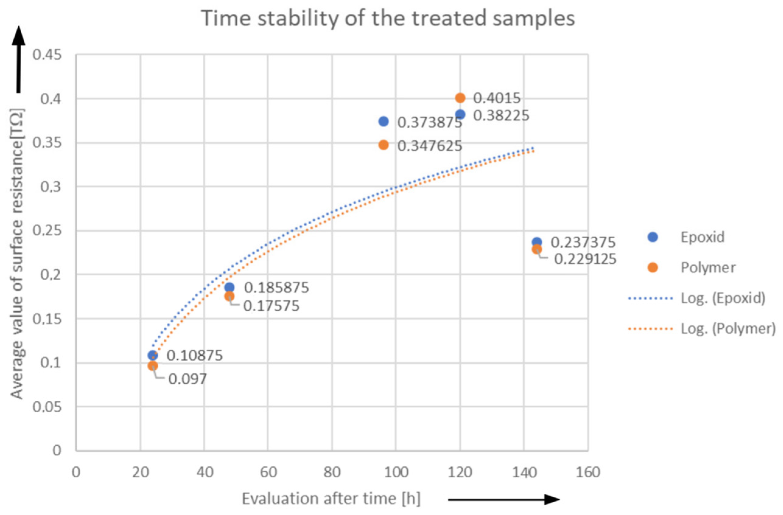
The reason for this was the indicated surface charge, which was only verified initially after plasma application and before the last measurement after 144 h (SIMCO FMX-004, ser.no. FX24585). The prepared tests already included a systematic measurement of the electrical charge. The surface treatment with plasma without precursors showed that in thermoplastic materials and thermosets, the surface resistance Rp rose and did not decrease with time; conversely, it stabilized at a higher level of values (Figure 17). The difference and properties of thermosets and thermoplastics had not been investigated, but both types of insulants demonstrated increased electrical surface strength. The hypothesis of a nano-treatment of the surface and the capture of the free electric charge propagating along the surface before the moment of discharge was verified by quantitative measurements. Furthermore, the effect of the retention of the electrical charge after plasma discharge application was demonstrated using a time-lapse surface strength measurement test after surface treatment. The results were obtained under ambient conditions (pressure, temperature, waviness, illumination, surface cleanliness, etc.) similar to industrial conditions for the expected deployment of the technique. Thus, the fundamental decision was that the dielectric surfaces were not specially treated or cleaned before the actual plasma application. For the measurements at 144 h after plasma discharge application, there was a statistically significant change in the parameters in an otherwise exponential trend (Figure 17). Here, there may have been a sample manipulation error during the indicative (no-)surface charge measurement. This fact will be verified in a forthcoming experiment.
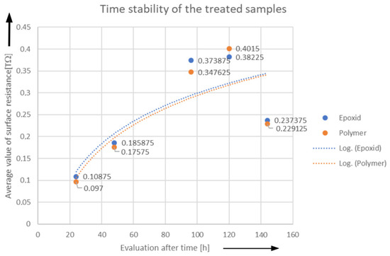
Figure 17.
Evaluation of the time stability of the first series of treated samples (N = 8) of both types of plastics (epoxy-based, polymer-based).
The evaluated surface jump intensities according to the proposed methodology were evaluated from the measured surface resistance shown in Figure 9 and Figure 10. The recalculated magnitudes of Ep intensities moved within a proportional range (Ep = 0.099–0.109 V/mm).
Further research will focus on selecting and applying the precursors; the effects on the surface resistance Rp and stability over time will also be investigated.
7. Conclusions
The proposed methodology for dielectric/insulator plasma surface treatment was repeatedly verified on sets of test samples. The repeatability and desired increase in the surface strength during the plasma treatment was demonstrated, together with the change in the intensity of the electric field on the surface of the sample at the post-treatment times; the effects and quantities were graphically represented. A parametric analysis of the plasma treatment was carried out in order to determine the maximum strength of the surface of the sample, Ep. The tests were repeated on other sets of samples, indicating the actual repeatability of the plasma treatment without the use of precursors. The procedures showed that the first treatment increased the parameters of the dielectric surface resistance (and thus the flashover resistance) within tens of percent for both the thermoset and the thermoplastic dielectrics.
The benefit of the research rests in a systematic, technologically manageable exposure of the insulator surface. In the process, the surface strength increased by an industrially usable value (up to 50% of the surface resistivity), and the gradually improved setting of the atmospheric plasma discharge allowed changing the surface parameters with a proven time stability.
At the next stages, our research will prominently involve applying precursors in plasma and evaluating their influence on the described traceable parameters of the dielectric, the aim being to refine the parameters of the surface properties of insulators.
Author Contributions
Conceptualization, P.F. and R.P.; methodology, R.P.; software, R.P.; validation, M.K., R.P. and P.F.; formal analysis, P.L. and R.P.; investigation, P.F.; resources, P.F. and P.L.; data curation, P.L. and R.P.; writing—original draft preparation, R.P.; writing—review and editing, P.F.; visualization, R.P. and P.F.; supervision, P.F.; project administration, P.F. and M.K.; funding acquisition, P.F. and M.K. All authors have read and agreed to the published version of the manuscript.
Funding
The research was funded within the National Sustainability Programme, from a Czech Science Foundation grant (GA 20-14105S) and grants BD 2020-2022, FEKT-S-20-6360, BD 2023-2025, FEKT-S-23-8425.
Institutional Review Board Statement
Not applicable.
Informed Consent Statement
Not applicable.
Data Availability Statement
Data is contained within the article.
Acknowledgments
For the actual analyses and experiments, the infrastructure of the SIX Centre was utilized.
Conflicts of Interest
The authors declare no conflict of interest.
References
- Kikuchi, H. Electrohydrodynamics in Dusty and Dirty Plasmas: Gravito-Electrodynamics and EHD; Springer: Dordrecht, The Netherlands, 2001; p. 227, ISBN 10:0792368223, ISBN 13:9780792368229. [Google Scholar]
- Fridman, A. Plasma Chemistry; Cambridge University Press: New York, NY, USA, 2008. [Google Scholar]
- Koinuma, H.; Ohkubo, H.; Hashimoto, T.; Inomata, K.; Shiraishi, T.; Miyanaga, A.; Hayashi, S. Development and application of a microbeam plasma generator. Appl. Phys. Lett. 1992, 60, 816–817. [Google Scholar] [CrossRef]
- Klíma, M.; Zajíčková, L.; Janča, J.; Schweiz, Z. The perspectives of plasmachemical treatment on ancient artifacts. Archäol. Kunstgesch. 1997, 54, 31. [Google Scholar]
- Raballand, V.; Benedikt, J.; von Keudell, A. Deposition of carbon-free silicon dioxide from pure hexamethyldisiloxane using an atmospheric microplasma jet. Appl. Phys. Lett. 2008, 92, 091502. [Google Scholar] [CrossRef]
- Drexler, P.; Fiala, P.; Klima, M.; Szabo, Z.; Dostal, L.; Kadlec, R.; Pernica, R. Electromagnetic Modeling of a Plasma Chamber: Theory and Experiments. In Proceedings of the 2021 Photonics & Electromagnetics Research Symposium (PIERS), Hangzhou, China, 21–25 November 2021; pp. 609–613. [Google Scholar]
- Schäfer, J.; Fricke, K.; Mika, F.; Pokorná, Z.; Zajíčková, L.; Foest, R. Liquid assisted plasma enhanced chemical vapour deposition with a non-thermal plasma jet at atmospheric pressure. Thin Solid Films 2017, 630, 71–78. [Google Scholar] [CrossRef]
- Beijer, P.A.C.; Sobota, A.; van Veldhuizen, E.M.; Kroesen, G.M.W. Multiplying probe for accurate power measurements on an RF driven atmospheric pressure plasma jet applied to the COST reference microplasma jet. J. Phys. D Appl. Phys. 2016, 49, 104001. [Google Scholar] [CrossRef]
- Klima, M.; Janča, J.; Kapička, V.; Slavíče, P.; Saul, P. Method of Making a Physically and Chemically Active Environment by Means of a Plasma Jet and the Related Plasma Jet. U.S. Patent US6525481B1, 25 February 2003. [Google Scholar]
- Klíma, M.; Slavíček, P.; Šíra, M.; Čižmár, T.; Vaněk, P. HF plasma pencil and DC diaphragm discharge in liquids—Diagnostics and applications. Czechoslov. J. Phys. 2006, 56, B1051–B1056. [Google Scholar] [CrossRef]
- Yablokov, M.; Gilman, A.; Kuznetsov, A. Modification of wettability of polymer surfaces by plasma. In Proceedings of the 21st Symposium on Application of Plasma Processes, Štrbské Pleso, Slovakia, 13–18 January 2017; Book of Contributed Papers. pp. 19–26. [Google Scholar]
- Norberg, S.A.; Johnsen, E.; Kushner, M.J. Helium atmospheric pressure plasma jets touching dielectric and metal surfaces. J. Appl. Phys. 2015, 118, 013301. [Google Scholar] [CrossRef]
- ANSYS. 1990–2023. Available online: www.ansys.com (accessed on 15 May 2019).
- Kopeček, J.; Dvořák, M. Přístrojové Transformátory; Academia: Praha, Czech Republic, 1966. [Google Scholar]
- Fiala, P. Modeling of Current Transformers on a Short-Circuit. Ph.D. Thesis, VUT FEI v Brně, Brno, Czechia, 1999. [Google Scholar]
- Havelka, O.; Dubravec, B.; Gross, B.; Homa, V. Novotn7 V. In Elektrické Přístroje; SNTL: Prague, Chech Republic, 1985. [Google Scholar]
- Vávra, Z.; Vaněk, J. Vysoké Napětí a Elektrické Přístroje, Laboratorní a Numerická Cvičení, Část II: Elektrické Přístroje; Elektronický Text; FEKT VUT v Brně: Brno, Czech Republic, 2003. [Google Scholar]
- Kříž, M. Dimenzování a Jištění Elektrických Zařízení; IN-EL, spol. s r.o.: Praha, Czech Republic, 2008. [Google Scholar]
- Bárta, K.; Vostracký, Z.; Pospíšil, V.; Ulč, M.; Zelenka, M. Spínací Přístroje Velmi Vysokého Napětí; SNTL-Nakladatelství Technické Literatury: Praha, Czech Republic, 1983. [Google Scholar]
- Havelka, O.; Vávra, Z.; Svoboda, D. Podklady a Příklady pro Navrhování Elektrických Přístrojů I; Ediční středisko VUT Brno: Brno, Czechia, 1985. [Google Scholar]
- Fiala, P. Effect of Insulating Layers on Electrodes on the Electric Field; Research Report; VUEP Brno: Brno, Czechia, 1989. [Google Scholar]
- Deng, J.; Matsuoka, S.; Kumada, A.; Hidaka, K.; Pu, L.; Zhang, G. Effect of residual charges on surface discharge propagation under impulse voltage. Gaodianya Jishu/High Volt. Eng. 2012, 38, 2137–2144. [Google Scholar] [CrossRef]
- Dong, J.N.; Du, B.X.; Li, J.; Liang, H.C.; Yao, H.; Chen, Y. Surface Charge and Electric Field Distribution along Tri-post Insulators in ±800 kV GIL. In Proceedings of the 2021 International Conference on Electrical Materials and Power Equipment (ICEMPE), Chongqing, China, 11–15 April 2021; pp. 1–4. [Google Scholar]
- Montanari, G.; Ciani, F.; Testa, L.; Guastavino, F.; Coletti, G.; Mulhaupt, R. Electric strength, space charge and surface discharge characterization of nanostructured epoxy-silicate insulating materials. In Proceedings of the 2005 International Symposium on Electrical Insulating Materials, 2005 (ISEIM 2005), Kitakyushu, Japan, 5–9 June 2005; Volume 1, pp. 206–209. [Google Scholar]
- Wang, H.; Xue, J.-Y.; Wang, Y.-B.; Su, G.-Q.; Deng, J.-B.; Mu, H.-B.; Zhang, G.-J. Improved algorithm of surface charge density distribution and electric field distribution on insulating materials. In Proceedings of the 2017 1st International Conference on Electrical Materials and Power Equipment (ICEMPE), Xi’an, China, 14–17 May 2017; pp. 332–335. [Google Scholar]
- Zhang, C.; Wan, K.; Wu, C.; Gan, H. Simulation study on the optimization of the surface electric field of laminated insulators with gradient dielectric materials. In Proceedings of the 2021 IEEE 2nd China International Youth Conference on Electrical Engineering (CIYCEE), Chengdu, China, 15–17 December 2021; pp. 1–5. [Google Scholar]
- Wetz, D.; Mankowski, J.; Kristiansen, M. The Impact of Electrode Area and Surface Roughness on the Pulsed Breakdown Strength Water. In Proceedings of the 2005 IEEE Pulsed Power Conference, Monterey, CA, USA, 13–15 June 2005; pp. 1163–1166. [Google Scholar]
- Wang, X.; An, Z.; Qin, Y. Physicochemical Characteristics and Basic Properties of the Fluorinated BOPP Surface Layer and its Effect on Dielectric Strength. In Proceedings of the 2021 IEEE International Conference on the Properties and Applications of Dielectric Materials (ICPADM), Johor Bahru, Malaysia, 12–14 July 2021; pp. 258–261. [Google Scholar]
- Li, G.; Ma, H.; Ding, J.; Liu, Z.; Wang, J.; Geng, Y. Relationship between Morphology Feature of Contact Surfaces and Impulse Breakdown Voltage in Vacuum Gap under a Non-uniform Electric Field. In Proceedings of the 2019 5th International Conference on Electric Power Equipment—Switching Technology (ICEPE-ST), Kitakyushu, Japan, 13–16 October 2019; pp. 437–440. [Google Scholar]
- Choi, J.-H.; Kim, S.-H.; Jang, K.; Hikita, M.; Lee, S.-H. Finite-Element Analysis for Surface Discharge Due to Interfacial Polarization at the Oil-Nanocomposite Interface. IEEE Trans. Magn. 2017, 54, 1–4. [Google Scholar] [CrossRef]
- Sharbaugh, A.H.; Cox, E.B.; Crowe, R.W.; Auer, P.L. The effect of electrode configuration on the electric strength of hexane. In Proceedings of the 1955 Conference on Electrical Insulation, Pocono Manor, PA, USA, 17–19 October 1955. [Google Scholar]
- Sami, A.; David, E.; Frechette, M.; Savoie, S. Breakdown and surface discharge involving PE/SiO2 nanocomposites. In Proceedings of the 2010 IEEE International Symposium on Electrical Insulation (ISEI), San Diego, CA, USA, 6–9 June 2010; pp. 1–4. [Google Scholar]
- Chen-Tsu, F.; Ai-Kang, L. The dependence of surface damage induced by electrical-discharge machining on the fracture strength of Al2O3-Cr3C2 composites. Mater. Chem. Phys. 1994, 39, 129–135. [Google Scholar] [CrossRef]
- Ma, D.; Siegel, R.W.; Hong, J.-I.; Schadler, L.S.; Mårtensson, E.; Önneby, C. Influence of nanoparticle surfaces on the electrical breakdown strength of nanoparticle-filled low-density polyethylene. J. Mater. Res. 2004, 19, 857–863. [Google Scholar] [CrossRef]
- Fiala, P.; Drexler, P.; Gescheidtová, E.; Klíma, M.; Zajíčková, L. A Plasma Chamber: Electromagnetic Modeling and Experiments. In Proceedings of the 2019 PhotonIcs & Electromagnetics Research Symposium—Spring (PIERS-Spring), Rome, Italy, 17–20 June 2019; pp. 2570–2573, ISBN 978-1-7281-3403-1. [Google Scholar]
- Drexler, P.; Szabó, Z.; Pernica, R.; Zukal, J.; Kadlec, R.; Klíma, M.; Fiala, P. Modeling and Experimental Verification of Plasma Jet Electromagnetic Signals. Modelling 2022, 3, 70–91. [Google Scholar] [CrossRef]
- Polášková, K.; Nečas, D.; Dostál, L.; Klíma, M.; Fiala, P.; Zajíčková, L. Self-organization phenomena in cold atmospheric pressure plasma slit jet. Plasma Sources Sci. Technol. 2022, 31, 125014. [Google Scholar] [CrossRef]
- Maryniak, W.A.; Uehara, T.; Noras, M.A. Surface Resistivity and Surface Resistance Measurements Using a Concentric Ring Probe Technique; Trek Application Note 1005; Advanced Energy: Denver, CO, USA, 2003. [Google Scholar]
- Amin, M. Methods for preparation of nano-composites for outdoor insulation applications. Rev. Adv. Mater. Sci. 2013, 34, 173–184. [Google Scholar]
- Khan, T.M.; Khan, S.U.-D.; Raffi, M.; Khan, R. Theoretical–Computational Study of Atmospheric DBD Plasma and Its Utility for Nanoscale Biocompatible Plasmonic Coating. Molecules 2021, 26, 5106. [Google Scholar] [CrossRef] [PubMed]
- Liang, H.; Du, B.; Li, J.; Du, Q. Numerical simulation on the surface charge accumulation process of epoxy insulator under needle-plane corona discharge in air. IET Sci. Meas. Technol. 2018, 12, 9–16. [Google Scholar] [CrossRef]
- Steinbauer, M.; Pernica, R.; Zukal, J.; Kadlec, R.; Bachorec, T.; Fiala, P. Modeling electromagnetic nanostructures and experimenting with nanoelectric elements to form periodic structures. Inform. Autom. Pomiary W Gospod. I Ochr. Sr. 2020, 10, 4–14. [Google Scholar] [CrossRef]
- Pernica, R.; Klima, M.; Szabó, Z.; Kadlec, R.; Londak, P.; Fiala, P. Plasma Discharge-based Treatment to Increase the Strength of a Dielectric Surface. In Proceedings of the 2023 Photonics & Electromagnetics Research Symposium (PIERS), Prague, Czech Republic, 3–6 July 2023; pp. 379–388. [Google Scholar]
- Fiala, P.; Ošmera, P.; Werner, P. Nano-Electric Structures, Modeling, and the Related Applications in Materials Science. In Proceedings of the 11th International Conference on Measurement Proceedings, Smolenice Castle, Slovakia, 29–31 May 2017; Institute of Measurement Science, Slovak Academy of Science: Bratislava, Slovakia, 2017; pp. 127–130, ISBN 978-80-972629-1-4. [Google Scholar]
- Polášková, K.; Ozkan, A.; Klíma, M.; Jeníková, Z.; Buddhadasa, M.; Reniers, F.; Zajíčková, L. Comparing efficiencies of polypropylene treatment by atmospheric pressure plasma jets. Plasma Process. Polym. 2023, 20, e202300031. [Google Scholar] [CrossRef]
- Polášková, K.; Klíma, M.; Jeníková, Z.; Blahová, L.; Zajíčková, L. Effect of Low Molecular Weight Oxidized Materials and Nitrogen Groups on Adhesive Joints of Polypropylene Treated by a Cold Atmospheric Plasma Jet. Polymers 2021, 13, 4396. [Google Scholar] [CrossRef] [PubMed]
- IEC 61340-5-1; Electrostatics—Part 5-1: Protection of Electronic Components against Electrostatic Effects—General Requirements, in Czech „Elektrostatika—Část 5-1: Ochrana elektronických součástek před elektrostatickými jevy—Všeobecné požadavky“. TECHNOR print, s.r.o.: Hradec Kralove, Czech Republic, 2001.
- ESD STM 11.11-2001; TEST REPORT, Tempo Static Dissipative High Density Polystyrene, Carriers, Report nu. 2002-003. River’s Edge Technical Service Carl Newberg: Rochester, MN, USA, 2001.
- ASTM Standard D 257-99; Standard Test Methods for DC Resistance or Conductance of Insulating Materials. ASTM International: West Conshohocken, PA, USA, 1999.


Disclaimer/Publisher’s Note: The statements, opinions and data contained in all publications are solely those of the individual author(s) and contributor(s) and not of MDPI and/or the editor(s). MDPI and/or the editor(s) disclaim responsibility for any injury to people or property resulting from any ideas, methods, instructions or products referred to in the content. |
© 2024 by the authors. Licensee MDPI, Basel, Switzerland. This article is an open access article distributed under the terms and conditions of the Creative Commons Attribution (CC BY) license (https://creativecommons.org/licenses/by/4.0/).