Article

Decoupled MPC Power Balancing Strategy for Coupled Inductor Flying Capacitor DC–DC Converter

1
China Academy of Aerospace Aerodynamics, Beijing 100086, China
2
School of Internet of Things Engineering, Jiangnan University, Wuxi 214122, China
*
Author to whom correspondence should be addressed.
Appl. Sci. 2024, 14(11), 4813; https://doi.org/10.3390/app14114813
Submission received: 28 April 2024 / Revised: 18 May 2024 / Accepted: 24 May 2024 / Published: 2 June 2024
(This article belongs to the Special Issue Challenges for Power Electronics Converters, 2nd Edition)

Abstract

:
A decoupled model predictive control (MPC) power balancing strategy for a coupled inductor-based flying capacitor DC–DC converter (FCDC) is a proposed to solve the power imbalance caused by the parameter differences in the coupled inductor. The decoupled mathematical model of coupled inductor FCDC is firstly derived by analyzing the converter operation state under various modes. On this basis, the control relationship between inductor current and flying capacitor (FC) voltage is redefined and an MPC power balance strategy based on the inductor current with single-step optimization is proposed. The proposed MPC strategy not only achieves decoupled power balancing control but also solves multi-objective dynamic optimization control of the inductor current and FC voltage, greatly reducing the computation load. A detailed theoretical analysis of the proposed strategy is presented and the balancing performance is effectively verified through the experiments.

1. Introduction

Renewable energy generation represented by photovoltaic and wind power has become a global trend in the development of electricity [1,2,3]. However, the intermittency of renewable energy has brought challenges to the stable operation of power grids. As an effective way to stabilize the power fluctuations, the electrochemical energy storage technique has been widely used in renewable energy generation systems [4,5,6], of which a bi-directional DC–DC converter is the core equipment. Due to the low voltage stress, small passive components, and common ground between input and output terminals, the flying capacitor three-level topology has certain advantages in medium- and high-voltage energy storage systems (ESSs) [7,8].
Interleaved parallel technology is often used in high-power energy storage applications [9,10]. To further improve power density, a coupled inductor is proposed to replace independent inductors to reduce system volume and weight [11]. However, in actual systems, manufacturing errors and differences in hardware circuits may cause impedance deviations between coupled circuits, resulting in phase-to-phase power imbalance. In [12,13,14], the power self-balancing characteristic of coupled inductor topology is researched. However, in cases of large perturbation, external strategies are required to achieve power balancing control. Ref. [15] proposed an integrated current balancing transformer for a two-phase DC–DC converter and the switches were achieved ZVS operation, yet this method is suitable only for low-power applications and the transformer design is complicated. To find an optimal DC–DC converter topology suitable for high-power applications, a three-phase interleaved DC–DC converter with coupled technique was proposed in [16], and a power balancing strategy was proposed by solving the matrix model of the converter [17]. To reduce the control order, a symmetrical coupled inductor design scheme for three-phase circuits was proposed in [18]. However, compared to that in [17], the overall inductor volume was not effectively optimized. Through the above analysis, although the coupled inductor helps to improve the system’s power density, the phase-to-phase power imbalance caused by the difference in the coupled parameters is still a key issue that needs to be addressed.
For FC topology, in addition to current control, it is also necessary to control the voltage of the FC to ensure it is half of the port-side voltage. Ref. [18] studied FC voltage self-balancing characteristics with small perturbations. Ref. [19] proposed an FC voltage control strategy based on an RLC circuit, which showed acceptable reliability. However, the auxiliary circuit weakens system reliability and increases system cost. Based on the average state equation, refs. [20,21] proposed the decoupled control strategy of output voltage and FC voltage sharing control using a PI algorithm for three-level and five-level FC topology. However, with the dynamic response speed of the linear regulator, it is hard to satisfy abrupt load changes. To address this issue, ref. [22] proposed a FC topology control method based on MPC. However, the multi-objective control brings a heavy computational load to the MPC strategy. Therefore, refs. [23,24,25] use mean square error, dynamic optimization, and artificial neural network methods, respectively, to estimate the optimal cost function, but these algorithms are complex to apply. Ref. [26] proposed an improved MPC algorithm for a bidirectional four-quadrant flying capacitor bi-directional DC–DC converter and derived a decoupled control model for the dual-side capacitor and inductor current, and achieved desired control performance. However, the three control objectives still impose a large computational load on system control.
Coupled inductor FCDC effectively improves the power density of an ESS, but the power imbalance issue caused by the parameter differences in the coupled inductor has not been solved. In this paper, a decoupled MPC power balancing strategy with single-step optimization for a two-phase coupled inductor FCDC is proposed. The proposed strategy not only achieves decoupled power balancing control but also solves the multi-objective dynamic optimization control issue of inductance current and FC voltage and greatly reduces the computational load. The proposed strategy has favorable power, balancing performance and dynamic performance, and has been effectively verified through experimental results.

2. Basic Principle Analysis of Coupled Inductor FCDC

The topology of the coupled inductor FCDC applied in an ESS is shown in Figure 1. The coupled inductor is introduced to the traditional flying capacitor topology constructing the two-phase interleaved structure [27]. La and Lb represent self-inductance, M is mutual inductance. The self and mutual inductance satisfy La = Lb = L, −1 < k = M/L < 0, k is the coupled coefficient, and ra and rb are the equivalent resistance of the inductor. Cfa and Cfb represent the flying capacitor. ia and ib are the current flowing through each phase.
Basic operating principle: As shown in Figure 1, ui represents the voltage on the high-voltage side and uo represents the voltage on the low-voltage side. The carrier of phase a and b shifts 90°. When the energy flows from ui to uo, FCDC operates under Buck mode, Sa1, Sa2, Sb1, and Sb2 are alternately turned on, and Sa3, Sa4, Sb3, and Sb4 are turned off. When the energy flows from uo to ui, FCDC operates under Boost mode. Then, Sa3, Sa4, Sb3, and Sb4 are alternately turned on and Sa1, Sa2, Sb1, and Sb2 are turned off. The coupling inductor helps to reduce the inductor volume, but it does not change the voltage gain of the FCDC, and the gain characteristics are the same as a traditional flying capacitor DC–DC converter [28]. Taking Buck mode as the example, based on the above modulation principle, the coupled inductor FCDC has a total of 14 operating states, as shown in Figure 2.
Under phase- shifting control, the switches take turns conducting. As shown in Figure 2a, when Sa1 conducts, energy flows through Cfa and supplies power to uo, while the diodes of Sb3 and Sb4 in phase b provide the current freewheel path. In Figure 2b, all the switches on the upper bridge arm are turned off, and the energy in the coupling inductor flows through the lower bridge arm diode for freewheeling. In Figure 2c, the high-voltage-side energy flows through the upper bridge arm of phase b to charge Cfb. Phase a operates in a freewheeling state, and the current flows through Sb3 and Sb4. In Figure 2d, Cfa is discharged through Sa2 and the body diodes of Sa4, while phase b operates in freewheeling mode. In Figure 2f, Cfb is discharged through Sb2 and the body diodes of Sb4, while phase a operates in freewheeling mode. Cfb discharges in Figure 2f, and the energy on the ui side is directly supplied to uo through Sa1 and Sa2. In Figure 2g, Cfb is discharged and ui charges Cfa. In Figure 2h, ui continues to charge Cfa, while the energy flows through the upper bridge arm switch of phase b to supply power to uo. In Figure 2i, ui simultaneously charges Cfa and Cfb. In Figure 2j, while charging Cfb, ui directly supplies power to uo through the upper bridge arm of phase a. In Figure 2k, ui charges Cfb and the energy in Cfa is released to the uo side. In Figure 2l, Cfa discharges while ui supplies power to uo through the upper bridge arm of phase b. Cfa and Cfb discharge simultaneously in Figure 2m. In Figure 2n, ui supplies power to uo simultaneously through the switches on the upper bridge arms of phase a and b.
Actually, the converter operating state is determined by the region of the duty ratio. Taking 0 < D < 0.5 as an example, it can be seen from Figure 3 that the coupled inductor FCDC contains a total of eight operating states.
According to the analysis method shown in Figure 3, the operating states of coupled inductor FCDC with other duty ratios are shown in Table 1.
Power imbalance issue: According to Figure 1, when the energy flows from the left side to the right side and the switches Sa1 and Sb1 are conducting simultaneously, the voltage equation of the coupled inductor FCDC can be expressed as:
u i = L a d i a d t + M d i b d t + r a i a + u o u i = M d i a d t + L b d i b d t + r b i b + u o
It can be seen that only when La = Lb and ra = rb is the two-phase current equal and the power between the two phases balanced. However, manufacturer errors and other reasons lead the parameter differences in the coupled inductor in practical applications, resulting in imbalanced power between phases. It not only leads to a current stress deviation of the switching devices but also easily leads to saturation of the magnetic component. In addition, the mutual inductance leads to the power coupling between the two phases, which increases the difficulty of system power control. Thirdly, the control strategy design based on the converter model should not only consider the operating states shown in Table 1 but should also consider the impact of the coupled inductor on the performance of the control strategy. Therefore, it is necessary to further research the decoupled model and study the decoupled power control strategy.

3. Decoupled MPC Power Balancing Strategy for Coupled Inductor FCDC

3.1. Decoupled Mathematical Model of Coupled Inductor FCDC

The mathematical model of the coupled inductor FCDC should be firstly derived to propose the decoupled MPC power balancing strategy. Taking 0 < D < 0.5 as an example, as shown in Table 2, the converter consists of eight operating states. Taking ia, ib, ufa, and ufb as the state variables, Ts is the switching period. Thus, the operation time of mode i, h, g, f, m, l, k, and j in each switching period can be derived as (0.75-db1)Ts, (db1-0.5)Ts, (0.75-da1)Ts, (da1-0.5)Ts, (0.75-db2)Ts, (db2-0.5)Ts, (0.75-da2)Ts, (da2-0.5)Ts. According to the operating states shown in Figure 2, writing the circuit state equations and combine them with the corresponding operating time, the average state equation of the coupled inductor FCDC with 0 < D < 0.5 can be derived as:
d d t i a i b u fa u fb = r a L a 0 d a 2 d a 1 L a 0 0 r b L b 0 d b 2 d b 1 L b d a 1 d a 2 C fa 0 0 0 0 d b 1 d b 2 C fb 0 0 × i a i b u fa u fb   + d a 1 L a 1 L a d b 1 L b 1 L b 0 0 0 0 u i u o M L a d i b d t M L b d i a d t 0 0
where ufa and ufb are the voltages of flying capacitors Cfa and Cfb, respectively.
Similarly, the average state equation of the coupled inductor FCDC operating in other duty ratio intervals can be obtained by the above method, and the result is the same as (2). From (2), the mutual inductance M leads to a coupling relationship between the two phases, affecting the power control performance and complicating the control strategy design. Therefore, it is necessary to decouple the converter model.
Writing (1) with Laplace transform, it yields:
U(s) = Z(s)I(s)
where Z(s) is the impedance matrix and it is expressed as:
Z ( s )   = r a + L a s M s M s r b + L b s
For the interleaved converter with independent inductor, the inverse matrix of the impedance matrix is a diagonal matrix. Thus, in order to decouple the mathematical model of the coupled inductor FCDC, the inverse matrix of Z(s) shown in (4) should be transformed into a second-order diagonal matrix.
Performing a similar diagonalization transformation on (4) yields:
Y(s) = Z−1(s) = P−1H(s)P
where:
P = 1 1 1 1 ,   P 1 = 1 / 2 1 / 2 1 / 2 1 / 2 H ( s ) = r a / [ r a + s ( L a + M ) ] 0 0 r b / [ r b + s ( L b M ) ]
Thus, the expressions for the voltage and current in (3) under the s domain can be rewritten as:
U ( s ) = r a + s ( L a + M ) 0 0 r b + s ( L b M ) I ( s )
Substituting (6) into (2) and rewriting the result with inverse Laplace transform, the expressions of inductor voltage and current in the time domain are obtained as follows:
u a u b = L a + M 0 0 L b M d i a d t d i b d t T + r a i a r b i b
As shown in (7), there is no coupling relationship for the basic voltage equation of the coupled inductor. Thus, substituting (7) into (2), we can have:
d d t i a i b u fa u fb = r a ( L a + M ) 0 d a 2 d a 1 ( L a + M ) 0 0 r b ( L b M ) 0 d b 2 d b 1 ( L b M ) d a 1 d a 2 C fa 0 0 0 0 d b 1 d b 2 C fb 0 0 × i a i b u fa u fb   + d a 1 ( L a + M ) 1 ( L a + M ) d b 1 ( L b M ) 1 ( L b M ) 0 0 0 0 u i u o
It can be seen from (8) that there is no coupling between the two phase circuits under the coupled inductor, that is, the mathematical model of coupled inductor FCDC has been decoupled.

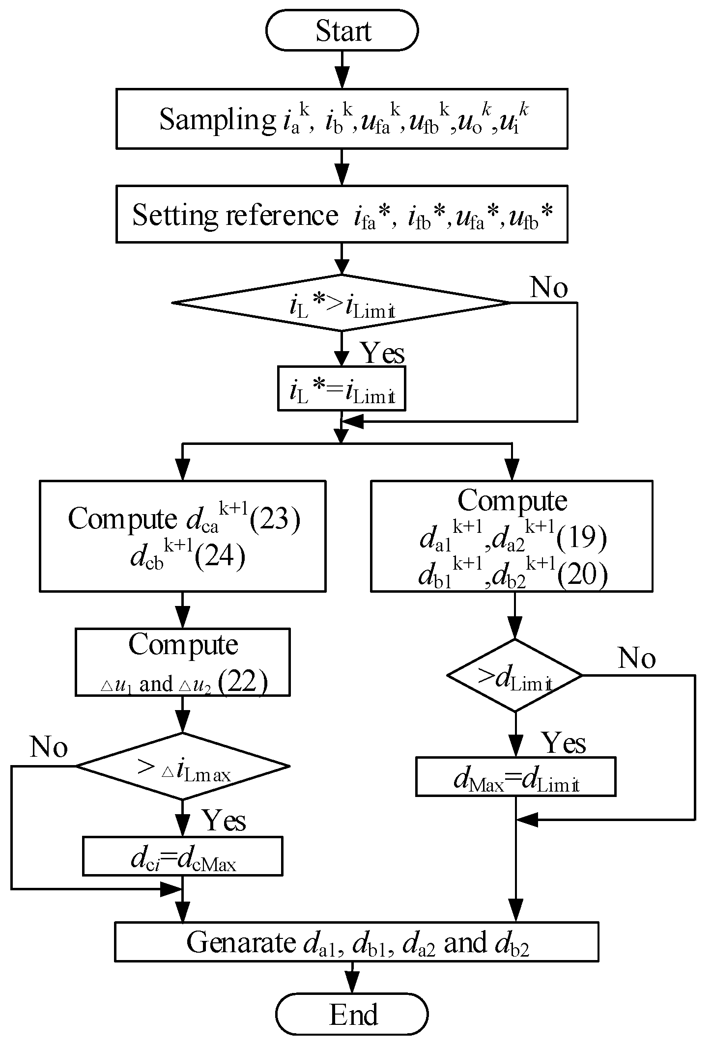
3.2. Multi-Objective MPC Strategy Design

The power balancing strategy needs to control both the current of each phase and the voltage of two flying capacitors. Under this requirement, by discretizing (8) with ia, ib, ufa and ufb as the control variables, the discrete models can be obtained as shown in Equation (10):
(9a) i a k + 1 = i a k i a k r a T s L a + M + ( d a 2 d a 1 ) T s L a + M u fa k + T s L a + M × d a 1 u i k u o k (9b) i b k + 1 = i b k i b k r b T s L b M + ( d b 2 d b 1 ) T s L b M u fb k + T s L b M × d b 1 u i k u o k (9c) u fa k + 1 = u fa k + ( d a 1 d a 2 ) T s C fa i a k (9d) u fb k + 1 = u fb k + ( d b 1 d b 2 ) T s C fb i b k
where the variables marked with k are the sampling value at the current time, and the symbols marked with k + 1 represent the predicted value at the next time step.
According to the traditional MPC algorithm, the cost function can be written as:
J k = λ 1 ( i a i a k + 1 ) 2 + λ 2 ( i b i b k + 1 ) 2 + λ 3 ( u fa u fa k + 1 ) 2 + λ 4 ( u fb u fb k + 1 ) 2
where the variables marked with * are the reference values and λ14 are the weight coefficients.
As shown in (11), in order to obtain the minimum Jk, it is not only necessary to calculate all combinations of the four duty ratios da1, da2, db1 and db2 but also to find the optimal solution for the four weight coefficients, which greatly increases the computational complexity. So, the traditional MPC control algorithm is not suitable for the control of the FCDC with coupled inductor.
Current control optimization: According to (8), the variation values of inductor current and flying capacitor voltage can be expressed as:
i a = r a ( L a + M ) i a + d a 2 d a 1 ( L a + M ) u fa + d a 1 ( L a + M ) u i 1 ( L a + M ) u o u fa = d a 1 d a 2 C fa u fa = d c C fa u fa
where △dc is the duty ratio to control FC voltage.
As shown in (12), when the converter is under the steady state, the flying capacitor voltage is unchanged and △dc is zero. At this time, the phase currents ia and ib are determined by da1 and db1, respectively, and are not affected the by flying capacitor. A small perturbation in flying capacitor voltage can cause variation in △dc, but its impact on the average current can be treated as affecting the current ripple, which can be negligible. Thus, when the current is taken as the control objective, the flying capacitor voltage in (11) can be simplified, and based on the decoupled mathematical model of the FCDC, the cost function in (11) can be rewritten as:
J a k = ( i a * i a k + 1 ) 2 J b k = ( i b * i b k + 1 ) 2
However, in order to achieve the minimum value of (13), it is necessary to calculate the predicted current values with different duty ratios according to (10). Even if the two cost functions are independent of each other, there is still a significant computational load.
Actually, (13) is a non-negative function. Assuming ui = 100 V, uo = 60 V, i a * = iak = 5 A and ufa = 50 V, the curves of different duty ratios based on (13) can be obtained and are shown in Figure 4.
It can be seen from Figure 4 that when the derivative value of Jak is zero, the minimum value is obtained. So, taking derivatives of Jak for da1k, da2k and taking derivatives of Jbk for db1k and db2k, respectively, we can have:
J a k d a 1 k d a 2 k = 1 = 2 ( i a * i a k + 1 ) ( i a k + 1 d a 1 k i a * d a 1 k ) J a k d a 2 k d a 1 k = 1 = 2 ( i a * i a k + 1 ) ( i a k + 1 d a 2 k i a * d a 2 k )
J b k d b 1 k d b 2 k = 1 = 2 ( i b * i b k + 1 ) ( i b k + 1 d b 1 k i b * d b 1 k ) J b k d b 2 k d b 1 k = 1 = 2 ( i b * i b k + 1 ) ( i b k + 1 d b 2 k i b * d b 2 k )
When the derivative value of Jak and Jbk to da1k, da2k and db1k, db2k is zero, the minimum value of the cost function shown in (13) can be obtained, and thus the duty ratio to control iak and ibk tracking the current reference can be derived. Assuming the equations shown in (14) are 0, we can have:
( i a k + 1 d a 1 k i a * d a 1 k ) 0 ( i a k + 1 d a 2 k i a * d a 2 k ) 0
Due to the predicted value being approximately equal to the steady-state reference, this yields:
i x * i x k i x k r x T s L x ± M + ( d x 2 d x 1 ) T s L x ± M u f x k + T s L x ± M × d x 1 u i k u o k
According to (17), it can be seen that the predicted value is approximately equal to the reference value, so:
i a * i a k + 1 0 i b * i b k + 1 0
Thus, da1k and da2k can be derived from (15) and (18). And the expression of da1k and da2k under Boost mode is shown in Appendix A.
d a 1 k = u o k u fa k + r a i a k u i k u fa k + L a + M i a * i a k T s u i k u fa k d a 2 k = u o k + u fa k u i k + r a i a k u fa k + L a + M i a * i a k T s u fa k
Similarly, the duty ratio for phase b can be expressed as:
d b 1 k = u o k u fb k + r b i b k u i k u fb k + L b M i b * i b k T s u i k u fb k d b 2 k = u o k + u fb k u i k + r b i b k u fb k + L b M i b * i b k T s u fb k
According to (18) and (19), the following conclusions can be drawn.
(1)
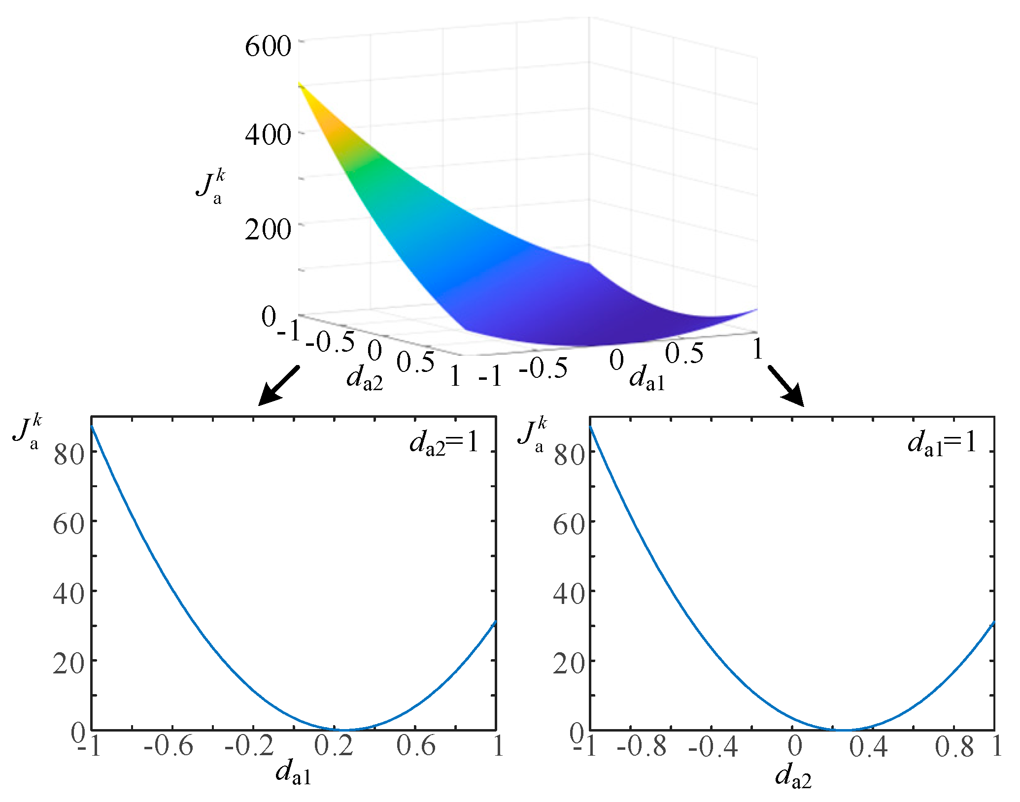
Taking phase a as an example, when the converter operates under steady-state iakia*, ufakuik/2 and uokuo*, we can have da1kda2k. Under this situation, da1k and da2k are derived by optimizing control ia, and ufa cannot be controlled by (19). The operation principle of phase b is the same as that of phase a.
(2)
With the aid of (19) and (20), the optimal duty ratio to track the current reference can be obtained through a single calculation, greatly reducing the computational burden.
Flying capacitor voltage control: Although the flying capacitor topology has voltage self-balancing ability [27], large perturbations will still cause flying capacitor voltage derivation. Hence, the FC voltage control has to be considered to ensure that the FC voltage is always controlled at half of the port voltage.
According to the operation states shown in Figure 2 and Table 1, the FC has charging and discharging processes in each control period. Assuming ufa* is the FC voltage reference, its expression can be written as:
u fa * = u fa k 1 2 Δ u 1 k + 1 2 Δ u 2 k
According to the FC charging and discharging circuit states, Δu1k and Δu2k can be expressed as:
Δ u 1 k = ( 1 d a 1 k d ca k ) T s 2 C fa i a k Δ u 2 k = ( 1 d a 1 k + d ca k ) T s 2 C fa i a k
where dcak is the duty ratio to control the flying capacitor voltage.
Substituting (22) into (21), the duty ratio dcak to control ufa can be derived as:
d ca k = 2 C fa T s i a k ( u fa * u fa k )
Similarly, the duty ratio dcbk to control ufb can be derived as:
d cb k = 2 C fb T s i b k ( u fb * u fb k )
Even if dcak and dcak only affect the current ripple, a large voltage deviation in the FC may affect the average value of the system current. Therefore, it is necessary to set constraints on (23) and (24) to obtain a satisfactory duty ratio for FC voltage control. Assuming the maximum current deviation is ∆iLlim, ∆df1k and ∆df2k must be limited to ∆Dlim, ensuring that the deviation of iL is within ∆iLlim. The relationship between ∆iLlim and ∆Dlim can be expressed as:
Δ D lim ( Δ i L lim 1 2 Δ i L ) 4 L T s ( u 2 * u 1 )
Thus, we can get the control block diagram of the proposed MPC power balancing strategy, as shown in Figure 5.

3.3. Stability Analysis

The direct Lyapunov method is employed in this paper to verify the stability of the proposed MPC strategy. This method indicates that when the function L(x) defined according to the system state variables x satisfies that L(x) is positive, L ˙ ( x ) is negative and lim x L ( x ) = , and thus the system is stable. So, according to the cost function, the discrete Lyapunov function can be defined as follows:
L ( x ) k = 1 2 [ x L err k + 1 ] T [ x L err k + 1 ]
where x is [ia ib]T.
Define the error variables between predicted and reference values as:
i a err k + 1 = i a k + 1 i a i b err k + 1 = i b k + 1 i b
According to (10), (26), and (27), the variation rate of L(x) as a function of the inductor current can be expressed as:
Δ L ( i x ) k = L ( i x ) k + 1 L ( i x ) k = 1 2 i x k i x k r x T s L x ± M + ( d x 1 d x 2 ) T s L x ± M u f x k + T s L x ± M × u i k + d x 2 1 u o k i x × i x k i x k r x T s L x ± M + ( d x 1 d x 2 ) T s L x ± M u f x k + T s L x ± M × u i k + d x 2 1 u o k i x 1 2 i x _ err k i x _ err k
where x represents phase a and b, respectively. When x represents phase a, the symbol ± should be written as +, and when x represents phase b, the symbol ± should be written as −.
When ∆df1k and ∆df2 do not reach the limit, the predicted value is approximately equal to the steady-state reference due to the tracking characteristics of MPC, as shown in (17). Substituting (17) into (28), we can have:
Δ L ( i x ) k = 1 2 i x _ err k i x _ err k
However, when ∆df1k or ∆df2k reaches the limit, the predicted current value will fail to track the reference. To address this issue, the adjustment of ∆iLlim should align with the changes in ΔL(x) to guarantee the stability and convergence of the variable’s control. The maximum current deviation can be optimized as follows:
Δ i L lim _ max = Δ i L lim + s ,   i f   Δ L ( i x ) k > 0 ; Δ i L lim ,   i f   Δ L ( i x ) k 0.
where s represents the increment step of current deviation.
The relaxation of ∆iLlim leads to a corresponding relaxation of ∆Dlim, thereby ensuring the sustained validity of Equation (29) within the system under these conditions.
As shown in (26) and (29), L(x) > 0 and L ˙ ( x ) < 0. Thus, based on the direct Lyapunov method, it can be known that the MPC strategy based on the cost function shown in (13) is stable.

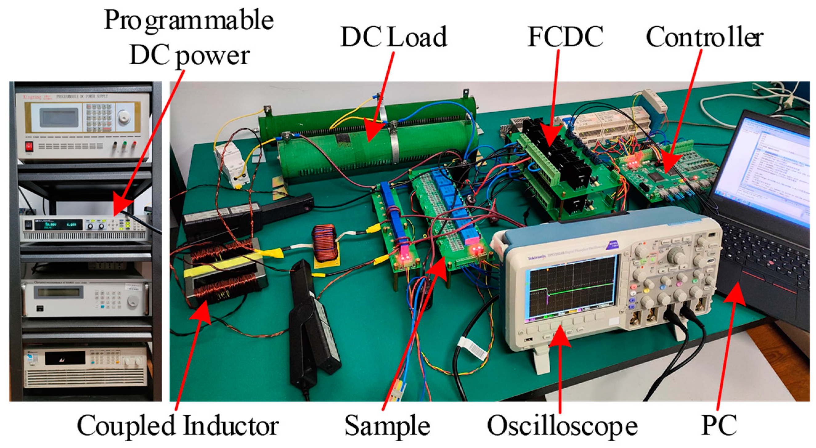
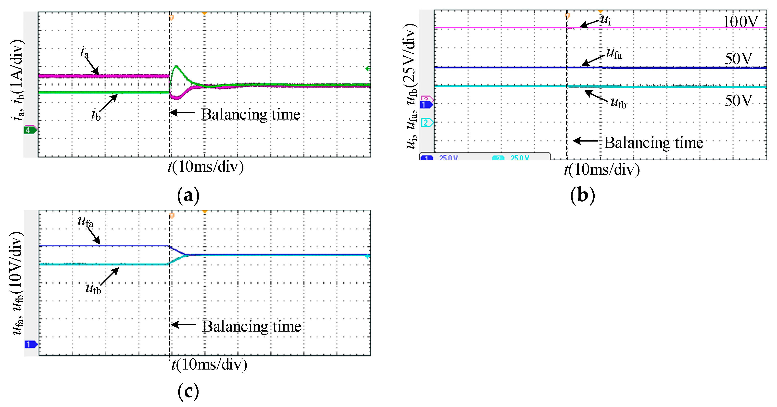
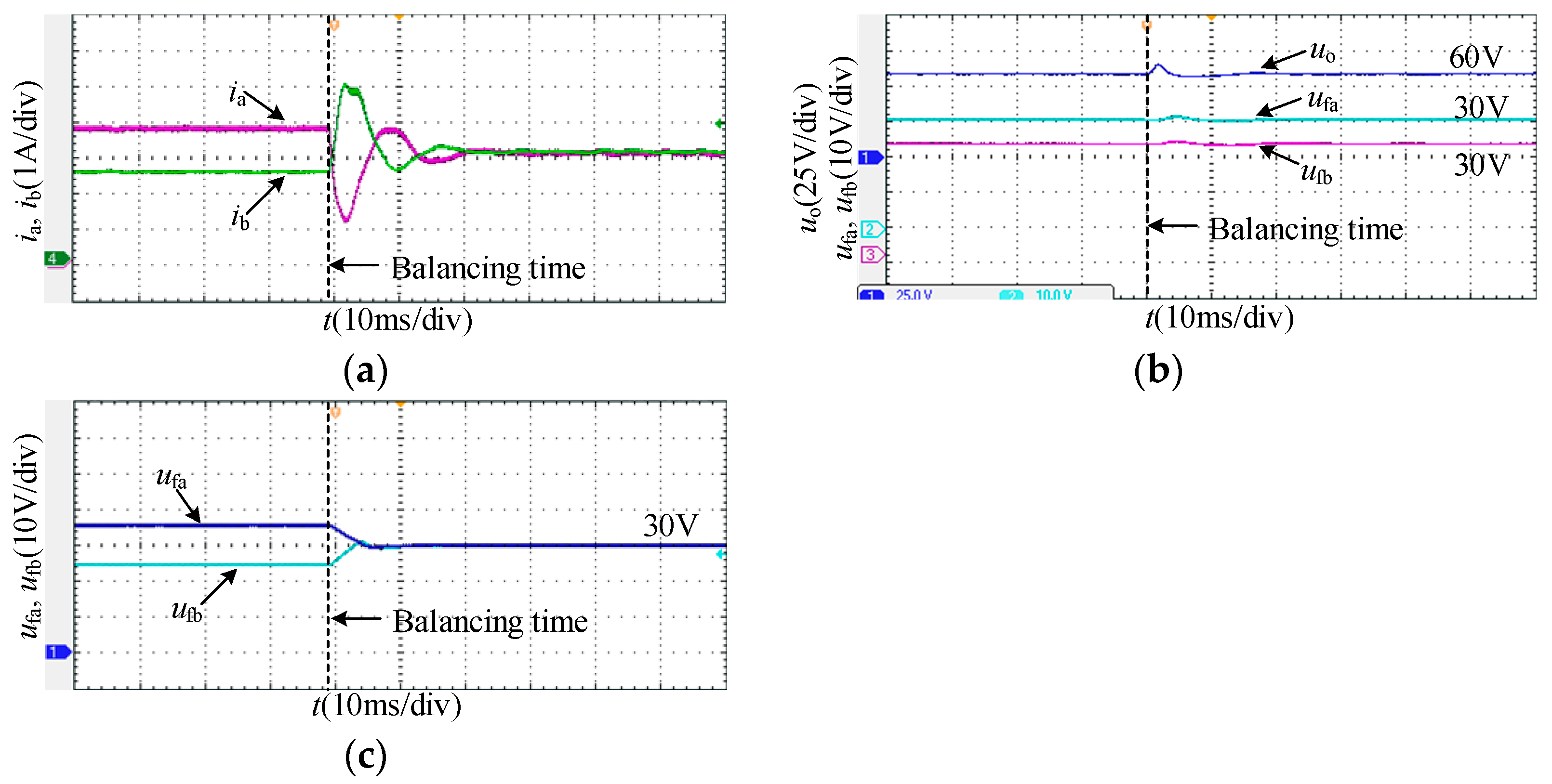
4. Experimental Verification

In order to verify the effectiveness of the proposed MPC power balancing strategy, an experimental platform is built in the laboratory, which is shown in Figure 6. A dual-core control architecture based on TMS320F28335 + XC3S500E is adopted, TMS320F28335 is responsible for sampling and calculation, while XC3S500E is responsible for generating PWM signals and achieving system protection. The experimental parameters are shown in Table 2. To simulate the imbalanced operation conditions, an inductor with 1 mH is connected in series in phase b.

4.1. Experimental Results

The output voltage under Buck mode is set to 50 V. The experimental results of the proposed power balancing MPC strategy under Buck mode are shown in Figure 7. Due to the unequal inductance between the two phases, ia and ib are imbalanced. As can be seen in Figure 7a, before the proposed strategy put into operation, ia is 3 A and ib is 2 A. After the control strategy is put into operation, the current reaches a balanced state within 10 ms. Compared to the initial state, the two-phase current is balanced by 20%. Figure 7b shows the voltage curves of Cfa and Cfb when the power balancing control is in action. It can be seen that the FC voltage is unchanged. Figure 7c shows the response curve of FC voltage from an imbalanced to a balanced state. Due to the direct regulation of flying capacitor voltage, the voltage difference between Cfa and Cfb quickly changes from 10 V to 0 V within 5 ms, achieving a balanced control state.
The input voltage under Boost mode is set to 50 V and the voltage on high voltage side is set to 60 V. The verification results are shown in Figure 8. Figure 8a shows that before the proposed strategy is put into operation, ia is 4 A and ib is 2.8 A. Due to the shoot-through state in Boost mode, the current change is more obvious than that in Buck mode, and it can be seen that ia and ib achieve balancing state within 20 ms at 3 A. The maximum current balancing regulation reaches 33%. Figure 8b shows the output voltage and FC voltage curves. Because the FC voltage is related to the output voltage under Boost mode, uo, ufa and ufb finally remain at 60 V, 30 V, and 30 V, respectively, after a short fluctuation. Figure 8c shows the FC voltage control response curve. It can be seen that the voltage difference between Cfa and Cfb quickly changes from 10 V to 0 V less than 5 ms, achieving a balanced control state.
The abrupt load changing results under Buck mode are shown in Figure 9. Figure 9a shows the loading results from 12 Ω to 6 Ω. Due to the differences in inductance, the two-phase current has different response curves, increasing from 1.6 A to 3.2 A. After a short oscillation within 22 ms, the two-phase current reaches a new balancing state and the voltage of flying capacitor remains controllable. The abrupt unloading results are shown in Figure 9b. The load resistor is changed from 6 Ω to 12 Ω. It can be seen that the current between phases can always remain balanced while the voltage of ufa and ufb is kept at 50 V.
The experimental results with load changing from 12 Ω to 6 Ω and from 6 Ω to 12 Ω under Boost mode are shown in Figure 10a,b. The inductance current increased from 1.5 A to 3 A under the loading condition and recovered to 1.5 A after unloading. It can be seen that both the current and voltage have favorable response performance: the current remains balanced and the FC voltage is controllable.
According to the above experimental results, it can be concluded that the proposed MPC power balancing strategy has favorable power balance performance to control the coupled inductor FCDC with imbalanced coupled inductor and can achieve FC voltage control. It can quickly respond to load power demands, maintain current balancing control, and ensure system stability.

4.2. Performance Discussion

Efficiency analysis: The converter efficiency is mainly determined by the switching loss. According to Figure 2 and Figure 3, it can be seen that the coupled inductor FCDC studied in this paper achieves Buck operation by chopping the upper bridge arm and keeping the lower bridge arm switch off. In Boost mode, the lower bridge arm switch operates under the chopping state, and the upper bridge switches are turned off. Therefore, its basic modulation method is the same as the flying capacitor topology controlled by a traditional PI strategy [20]. The MPC control strategy proposed in the paper is fixed frequency control, and the switching frequency is not affected by the control algorithm, so there will be no additional losses due to frequency changes. In addition, the control variable generated by the MPC strategy is the duty ratio, and the switch does not operate in soft switching mode. Therefore, we can say that the loss of the proposed MPC strategy is basically the same as that of the traditional PI control strategy.
Comparison with other strategies: The MPC strategy has better dynamic performance compared to traditional PI control. The proposed MPC strategy in the paper mainly solves the power imbalance issue under coupled inductance and the control of flying capacitor voltage. Compared with the coupled inductance balancing strategy proposed in [16], according to the experimental results shown in Figure 7, Figure 8, Figure 9 and Figure 10, it can be seen that the proposed MPC strategy has favorable balancing performance, with a two-phase current difference close to 0 under a steady state and dynamic load changes. Meanwhile, according to the voltage response curve of the flying capacitor proposed in [18], it can be seen that under similar operating conditions, the response time of the strategy is longer than 500 ms, while the response time of the MPC strategy proposed in this paper is about 10 ms and the capacitor voltage response time is about 5 ms. In comparison, the proposed strategy has obvious advantages in both balancing performance and dynamic response performance.

5. Conclusions

This paper proposes a decoupled MPC power balancing strategy to address the power imbalance issue caused by parameter differences in a coupled inductor FCDC. The decoupled mathematical model of the converter is studied first, and the basic principle of the proposed MPC power balancing strategy is derived by analyzing the relationship between system current and FC voltage control. By solving the constraint function, independent single-step optimization control of system current is proposed, At the meantime, the effective control of FC voltage is realized based on the time deviation of capacitor charging and discharging and combined with current ripple constraints. The proposed MPC power balancing strategy optimizes the multi-objective control of a coupled inductor FCDC, realizes power balancing control and FC voltage control, and greatly reduces the computing load. Experimental results also fully demonstrate that the proposed strategy has favorable current and voltage control capabilities and can achieve fast power balancing control.

Author Contributions

Methodology, X.W.; Software, K.B.; Validation, G.L.; Formal analysis, W.L.; Resources, J.C. All authors have read and agreed to the published version of the manuscript.

Funding

This research received no external funding.

Institutional Review Board Statement

Not applicable.

Informed Consent Statement

Not applicable.

Data Availability Statement

Data is contained in the article.

Conflicts of Interest

The authors declare no conflict of interest.

Appendix A

The average state equation of the coupled inductor FCDC under Boost mode is shown in (A1).
d d t i a i b u fa u fb = r a ( L a + M ) 0 d a 4 d a 3 ( L a + M ) 0 0 r b ( L b M ) 0 d b 4 d b 3 ( L b M ) d a 3 d a 4 C fa 0 0 0 0 d b 3 d b 4 C fb 0 0 × i a i b u fa u fb     + 1 ( L a + M ) d a 3 1 ( L a + M ) 1 ( L b M ) d b 3 1 ( L b M ) 0 0 0 0 u i u o
According to (A1), the discrete model of the control variable under Boost mode can be obtained as shown in (A2):
i a k + 1 = i a k i a k r a T s L a + M + ( d a 1 d a 2 ) T s L a + M u fa k + T s L a + M × u i k + d a 2 1 u o k i b k + 1 = i b k i b k r b T s L b M + ( d b 1 d b 2 ) T s L b M u fb k + T s L b M × u i k + d b 2 1 u o k u fa k + 1 = u fa k + ( d a 2 d a 1 ) T s C fa i a k u fb k + 1 = u fb k + ( d b 2 d b 1 ) T s C fb i b k
According to the cost function shown in (13), (19), and (20), we can obtain the partial derivatives of Jak under Boost mode as shown in (A3).
J a k d a 1 k d a 2 k = 1 = 2 ( i a * i a k + 1 ) ( i a k + 1 d a 1 k i a * d a 1 k ) J a k d a 2 k d a 1 k = 1 = 2 ( i a * i a k + 1 ) ( i a k + 1 d a 2 k i a * d a 2 k )
Solving (A3) with the method used under Buck mode, we can have:
d a 1 k = u fa k u i k + r a i a k u fa k + L a + M i a * i a k u fa k T s d a 2 k = u o k u fa k u i k + r a i a k u o k u fa k + L a + M i a * i a k ( u o k u fa k ) T s
With the aid of the FC voltage control equation shown in (27) and (28), the FC voltage under Boost mode can be controlled, and thus the MPC power balancing control algorithm for the coupled inductor FCDC under Boost mode is derived.

References

  1. Yang, Z.; Zhan, M.; Liu, D.; Ye, C.; Cao, K.; Cheng, S. Small-Signal Synchronous Stability of a New-generation Power System with 100% Renewable Energy. IEEE Trans. Power Syst. 2022, 38, 4269–4280. [Google Scholar] [CrossRef]
  2. Holttinen, H.; Kiviluoma, J.; Flynn, D.; Smith, J.C.; Orths, A.; Eriksen, P.B.; Cutululis, N.; Soder, L.; Korpas, M.; Estanqueiro, A.; et al. System Impact Studies for Near 100% Renewable Energy Systems Dominated by Inverter Based Variable Generation. IEEE Trans. Power Syst. 2020, 37, 3249–3258. [Google Scholar] [CrossRef]
  3. Xiong, L.; Liu, X.; Liu, Y.; Zhuo, F. Modeling and Stability Issues of Voltage-source Converter-dominated Power Systems: A Review. CSEE J. Power Energy Syst. 2022, 8, 1530–1549. [Google Scholar]
  4. Fan, H.; Zhou, S.; Wei, Q.; Hu, X. Honeycomb-like carbon for electrochemical energy storage and conversion. Renew. Sustain. Energy Rev. 2022, 165, 112585. [Google Scholar] [CrossRef]
  5. Argyrou, M.C.; Christodoulides, P.; Kalogirou, S.A. Energy storage for electricity generation and related processes: Technologies appraisal and grid scale applications. Renew. Sustain. Energy Rev. 2018, 94, 804–821. [Google Scholar] [CrossRef]
  6. Rocabert, J.; Capo-Misut, R.; Munoz-Aguilar, R.S.; Candela, J.I.; Rodriguez, P. Control of Energy Storage System Integrating Electrochemical Batteries and Supercapacitors for Grid-Connected Applications. IEEE Trans. Ind. Appl. 2018, 55, 1853–1862. [Google Scholar] [CrossRef]
  7. Chen, H.; Wang, D.; Tang, S.; Yin, X.; Wang, J.; Shen, Z.J. Continuous Control Set Model Predictive Control for Three-Level Flying Capacitor Boost Converter with Constant Switching Frequency. IEEE J. Emerg. Sel. Top. Power Electron. 2021, 9, 5996–6007. [Google Scholar] [CrossRef]
  8. Ye, Z.; Lei, Y.; Liao, Z.; Pilawa-Podgurski, R.C.N. Investigation of Capacitor Voltage Balancing in Practical Implementations of Flying Capacitor Multilevel Converters. IEEE Trans. Power Electron. 2022, 37, 2921–2935. [Google Scholar] [CrossRef]
  9. Zhang, J.; He, Y.; Hang, L. A Novel Interleaved Parallel Cascaded Three-Level PFC with Low Inductance Volt-Second and Low Common-Mode Noise. IEEE Trans. Power Electron. 2023, 38, 17–21. [Google Scholar] [CrossRef]
  10. Jovanovic, D.P.; Broadmeadow, M.A.H.; Taylor, R.R.; Walker, G.R.; Ledwich, G.F. Decoupling of Current Balancing and Reference Tracking Control in Parallel Interleaved Converters. IEEE Trans. Power Electron. 2020, 35, 4286–4295. [Google Scholar] [CrossRef]
  11. Lu, S.; Mu, M.; Jiao, Y.; Lee, F.C.; Zhao, Z. Coupled Inductors in Interleaved Multiphase Three-Level DC–DC Converter for High-Power Applications. IEEE Trans. Power Electron. 2016, 31, 120–134. [Google Scholar] [CrossRef]
  12. Moradisizkoohi, H.; Elsayad, N.; Mohammed, O.A. An Integrated Interleaved Ultrahigh Step-Up DC–DC Converter Using Dual Cross-Coupled Inductors with Built-In Input Current Balancing for Electric Vehicles. IEEE J. Emerg. Sel. Top. Power Electron. 2020, 8, 644–657. [Google Scholar] [CrossRef]
  13. Mayer, R.; El Kattel, M.B.; Oliveira, S.V.G. Multiphase Interleaved Bi-directional DC/DC Converter with Coupled Inductor for Electrified-Vehicle Applications. IEEE Trans. Power Electron. 2021, 36, 2533–2547. [Google Scholar] [CrossRef]
  14. Naseem, N.; Cha, H. Quad-Active-Bridge Converter with Current Balancing Coupled Inductor for SST Application. IEEE Trans. Power Electron. 2021, 36, 12528–12539. [Google Scholar] [CrossRef]
  15. Dou, Y.; Ouyang, Z.; Anderson, M.A.E. Integrated Coupled Inductors with Functionality of Current Balancing Transformer for Two-Phase Synchronous DC–DC Converters. IEEE Trans. Power Electron. 2020, 35, 4472–4476. [Google Scholar] [CrossRef]
  16. Pan, T.; Wang, Y.; Qu, Z.; Tao, W. Topology optimisation and current sharing strategy of interleaved bidirectional dc/dc converter with coupling technique. IET Power Electron. 2018, 11, 2470–2480. [Google Scholar] [CrossRef]
  17. Capella, G.J.; Pou, J.; Ceballos, S.; Zaragoza, J.; Agelidis, V.G. Current-Balancing Technique for Interleaved Voltage Source Inverters with Magnetically Coupled Legs Connected in Parallel. IEEE Trans. Ind. Electron. 2015, 62, 1335–1344. [Google Scholar] [CrossRef]
  18. McGrath, B.P.; Holmes, D.G. Analytical modeling of voltage balance dynamics for a flying capacitor multilevel converter. IEEE Trans. Power Electron. 2008, 23, 543–550. [Google Scholar] [CrossRef]
  19. Stala, R. The switch-mode flying-capacitor dc-dc converters with improved natural balancing. IEEE Trans. Ind. Electron. 2010, 57, 1369–1382. [Google Scholar] [CrossRef]
  20. Chen, H.-C.; Lu, C.-Y.; Lien, W.-H. Active Capacitor Voltage Balancing Control for Three-Level Flying Capacitor Boost Converter Based on Average-Behavior Circuit Model. IEEE Trans. Ind. Appl. 2019, 55, 1628–1638. [Google Scholar] [CrossRef]
  21. Lu, C.-Y.; Lin, D.-H.; Chen, H.-C. Decoupled Design of Voltage Regulating and Balancing Controls for Four-Level Flying Capacitor Converter. IEEE Trans. Ind. Electron. 2021, 68, 12152–12161. [Google Scholar] [CrossRef]
  22. Jayan, V.; Ghias, A.; Merabet, A. Modeling and control of three level bi-directional flying capacitor DC–DC converter in DC microgrid. In Proceedings of the 45th Annual Conference of the IEEE Industrial Electronics Society, Lisbon, Portugal, 14–17 October 2019; pp. 4113–4118. [Google Scholar]
  23. Thielemans, S.; Vyncke, T.J.; Melkebeek, J.A.A. Weight factor selection for model-based predictive control of a four-level flying capacitorinverter. IET Power Electron. 2012, 5, 323–333. [Google Scholar] [CrossRef]
  24. Davari, S.A.; Khaburi, D.A.; Kennel, R. An improved FCS-MPC algorithm for an induction motor with an imposed optimized weighting factor. IEEE Trans. Power Electron. 2012, 27, 1540–1551. [Google Scholar] [CrossRef]
  25. Dragi, T.; Novak, M. Weighting factor design in model predictive control of power electronic converters: An artificial neural network approach. IEEE Trans. Ind. Electron. 2019, 66, 8870–8880. [Google Scholar]
  26. Bi, K.; Lv, H.; Chen, L.; Li, J.; Zhu, Y.; Huang, W.; Fan, Q. A Model Predictive Controlled Bidirectional Four Quadrant Flying Capacitor DC/DC Converter Applied in Energy Storage System. IEEE Trans. Power Electron. 2022, 37, 7705–7717. [Google Scholar] [CrossRef]
  27. Ruan, X.; Li, B.; Chen, Q.; Tan, S.C.; Tse, C.K. Fundamental considerations of three-level DC–DC converters: Topologies analyses and control. IEEE Trans. Circuits Syst. I Regul. Pap. 2008, 55, 3733–3743. [Google Scholar] [CrossRef]
  28. Meynard, T.A.; Foch, H.; Thomas, P.; Courault, J.; Jakob, R.; Nahrstaedt, M. Multicell converters: Basic concepts and industry applications. IEEE Trans. Ind. Electron. 2002, 49, 955–964. [Google Scholar] [CrossRef]
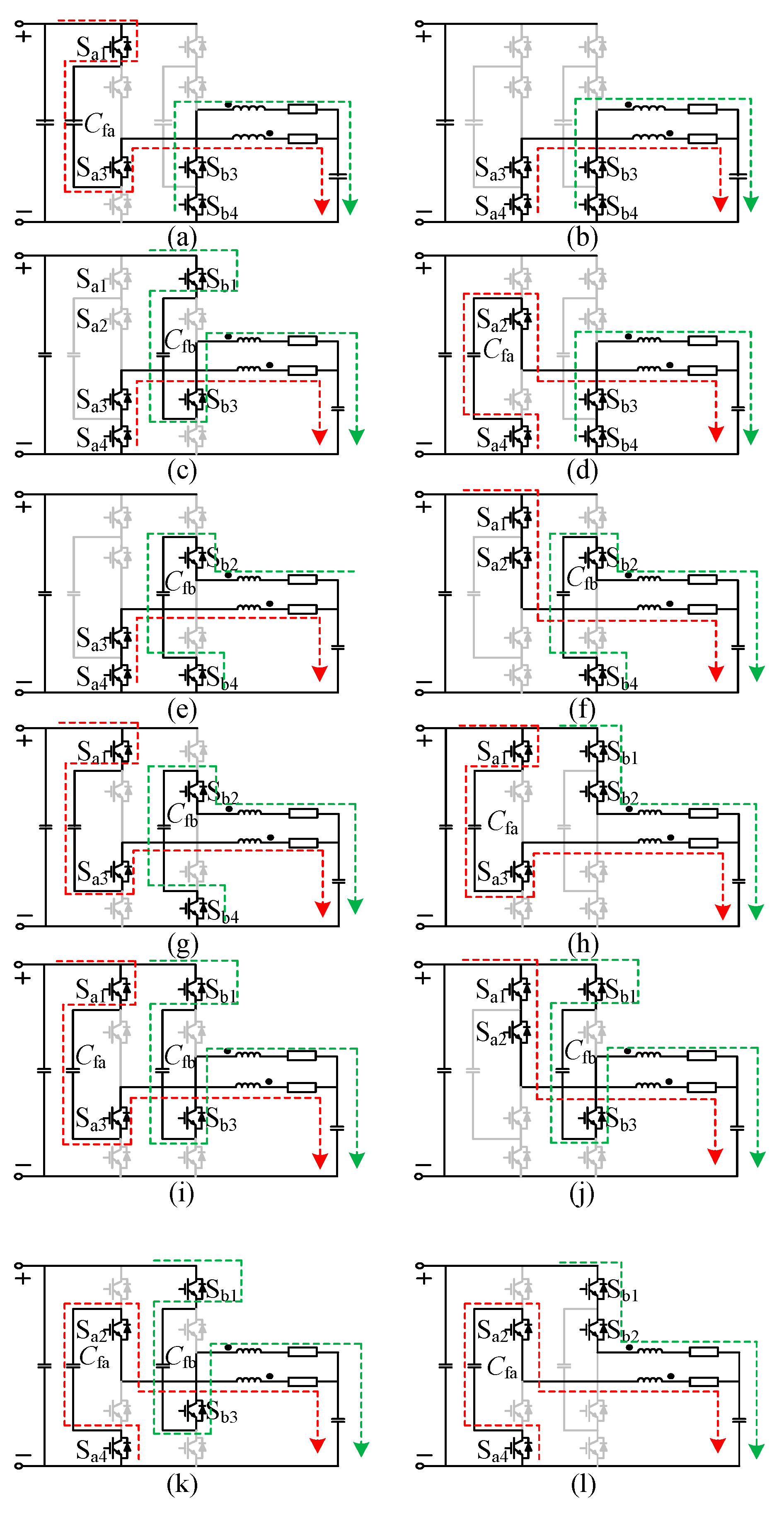
Figure 1. Topology of coupled inductor FCDC.
Applsci 14 04813 g001
Figure 2. Operating states of coupled inductor FCDC. (a) Mode 1. (b) Mode 2. (c) Mode 3. (d) Mode 4. (e) Mode 5. (f) Mode 6. (g) Mode 7. (h) Mode 8. (i) Mode 9. (j) Mode 10. (k) Mode 11. (l) Mode 12. (m) Mode 13. (n) Mode 14.
Applsci 14 04813 g002aApplsci 14 04813 g002b
Figure 3. Operating states of coupled inductor FCDC when 0 < D < 0.5.
Applsci 14 04813 g003
Figure 4. Curves of Jak with different duty ratios.
Applsci 14 04813 g004
Figure 5. Control block diagram of the proposed MPC power balancing strategy.
Applsci 14 04813 g005
Figure 6. Experimental platform.
Applsci 14 04813 g006
Figure 7. Experimental results under Buck mode. (a) Current balance response curves. (b) FC voltage response curves with current balancing control. (c) FC voltage balancing response curves.
Applsci 14 04813 g007
Figure 8. Experimental results under Boost mode. (a) Current balancing response curves. (b) FC voltage response curves with current balancing control. (c) FC voltage balancing response curves.
Applsci 14 04813 g008
Figure 9. Abrupt load changing results under Buck mode. (a) Abrupt loading. (b) Abrupt unloading.
Applsci 14 04813 g009
Figure 10. Abrupt load changing results under Boost mode. (a) Abrupt loading. (b) Abrupt unloading.
Applsci 14 04813 g010
Table 1. Operating states of coupled inductor FCDC with different duty ratios.
Duty Ratio RangeOperating State
−1 < D < −0.5a, b, c, d, e
D = −0.5a, c, d, e
−0.5 < D < 0a, c, d, e, g, i, k, m
D = 0g, i, k, m
0 < D < 0.5f, g, h, i, j, k, l, m
D = 0.5f, h, j, l
0.5 < D < 1f, h, j, l, n
Table 2. Experimental parameters.
ItemValueUnit
Maximum input voltage100V
Maximum operating power300W
Switching frequency10kHz
Self-inductance of phase a and b1mH
Mutual inductance−0.33mH
Flying capacitor220μF
Output voltage under Buck mode50V
Load12Ω
Disclaimer/Publisher’s Note: The statements, opinions and data contained in all publications are solely those of the individual author(s) and contributor(s) and not of MDPI and/or the editor(s). MDPI and/or the editor(s) disclaim responsibility for any injury to people or property resulting from any ideas, methods, instructions or products referred to in the content.

