
Analysis of Wafer Warpage in Diamond Wire Saw Slicing Sapphire Crystal


Abstract
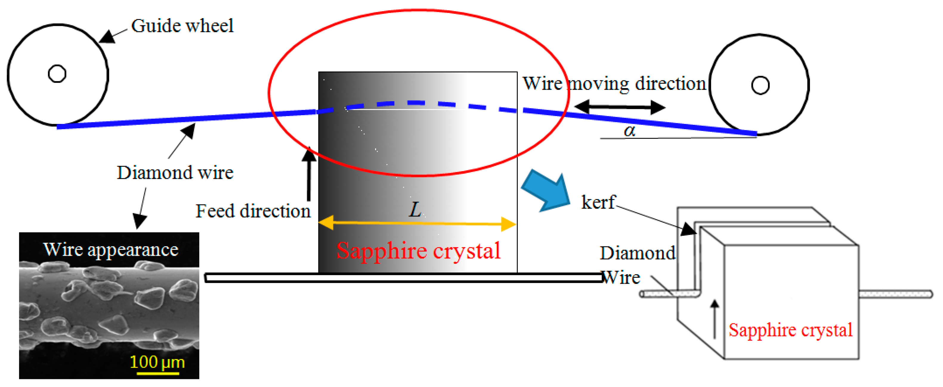
:1. Introduction
2. Theoretical Analyses
2.1. Heat Flux
2.2. Mathematical Model of the Temperature Field
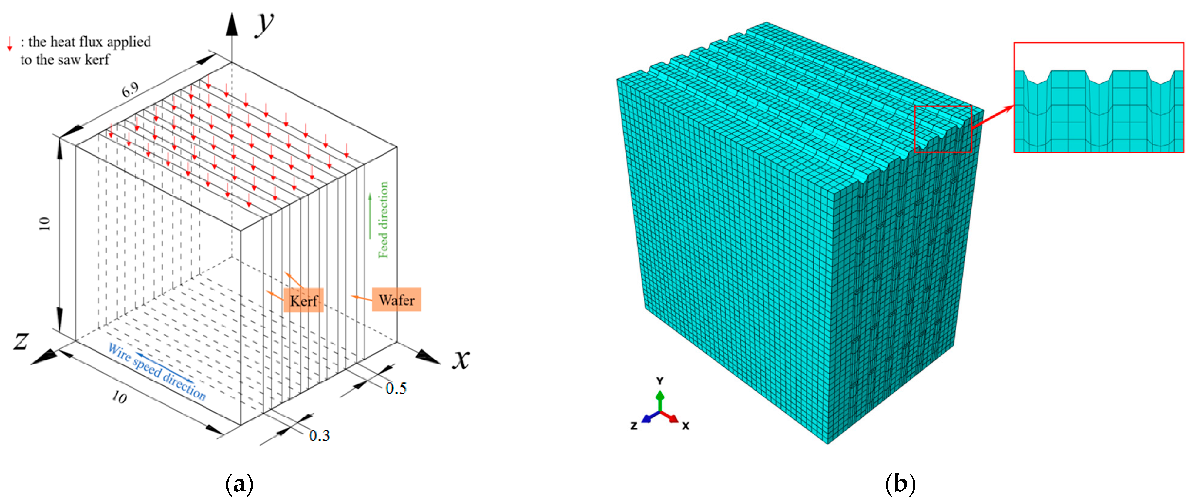
3. Finite Element Modeling
3.1. Material
3.2. Modeling and Solution
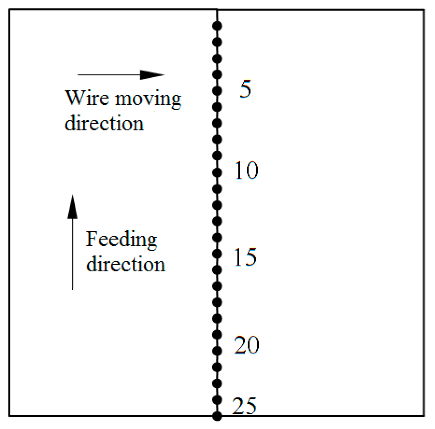
3.3. Calculation of Wafer Warpage Based on Finite Element Method
4. Sawing Experiment
5. Results and Discussion
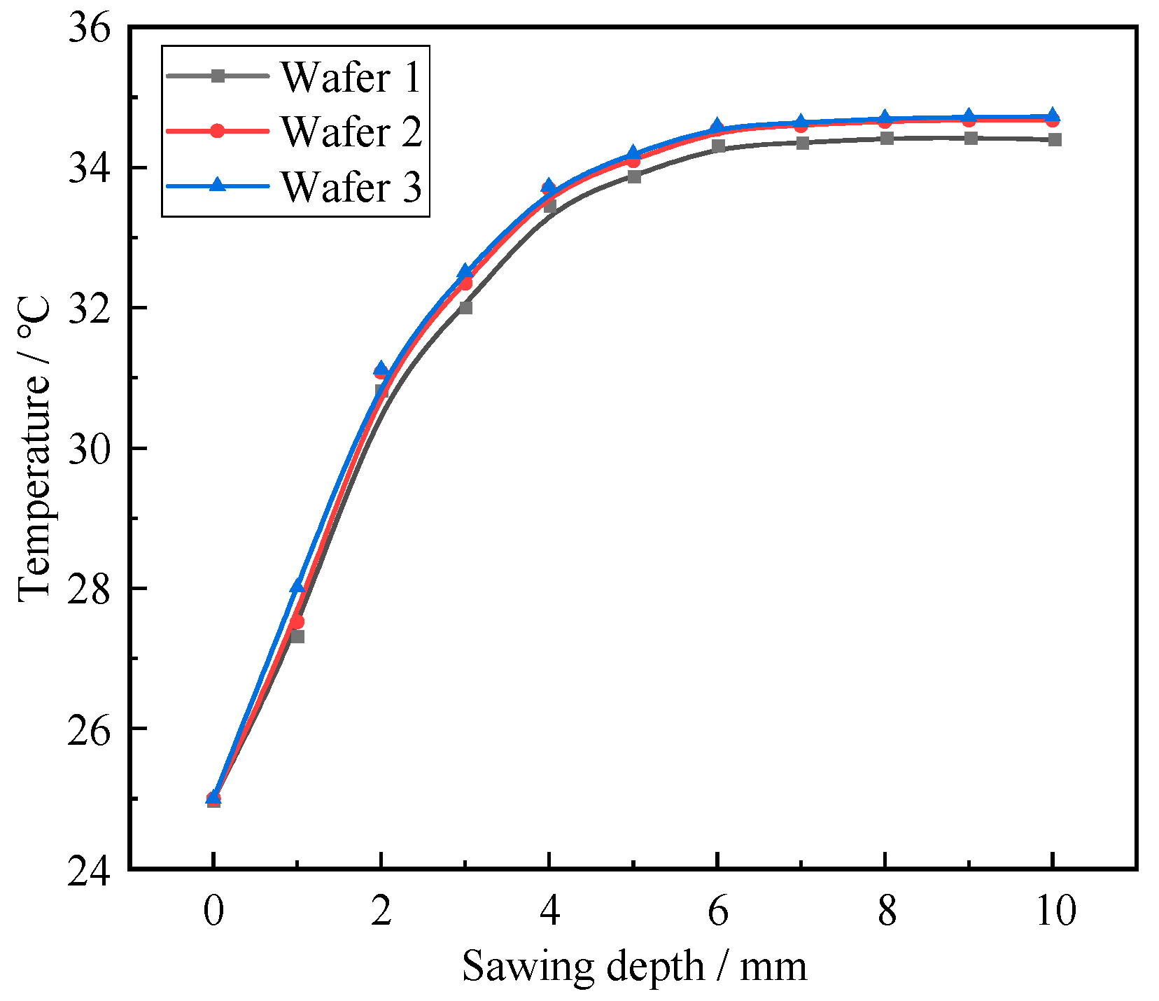
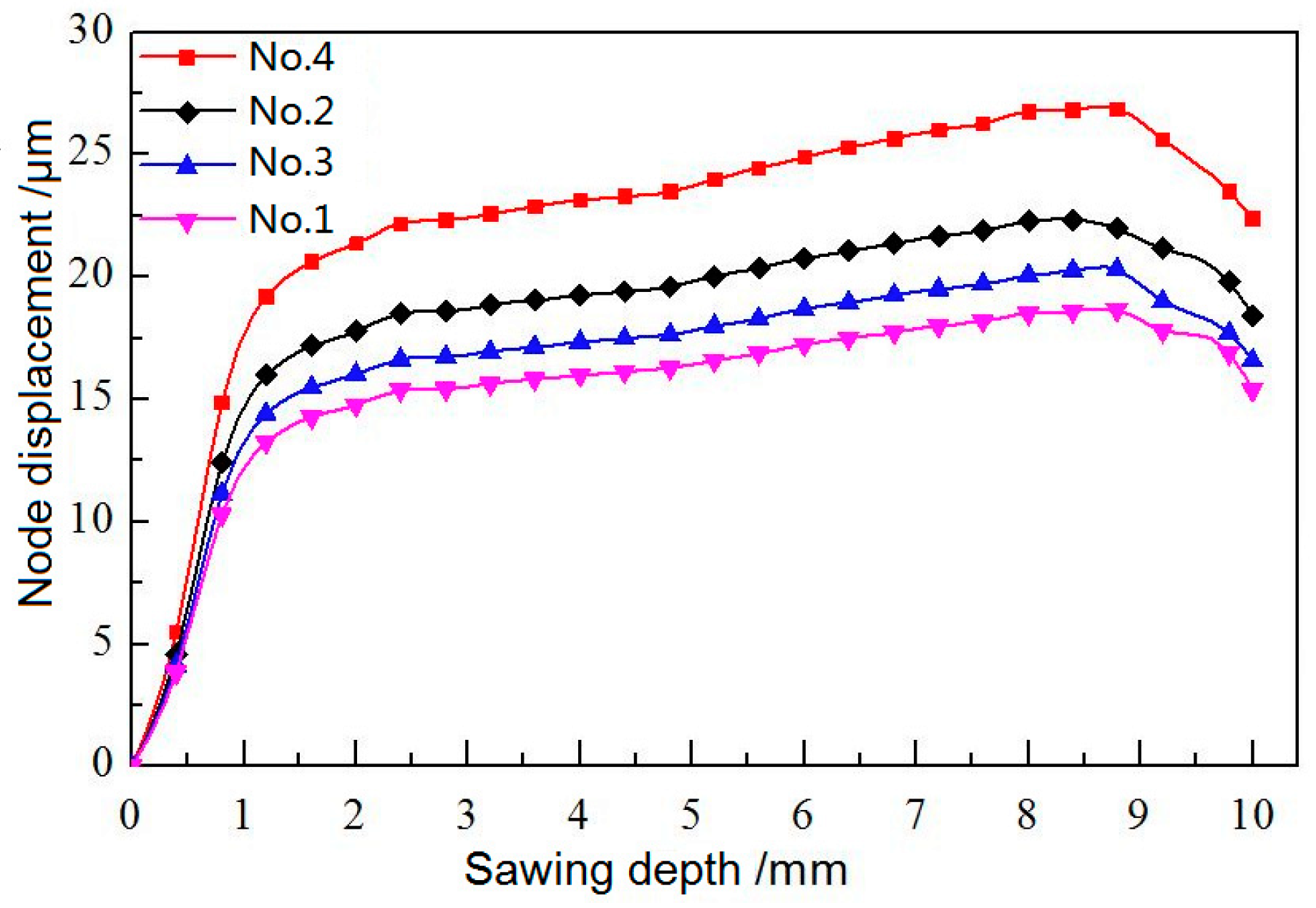
5.1. Analysis of Wafer Temperature Field and Thermal Deformation
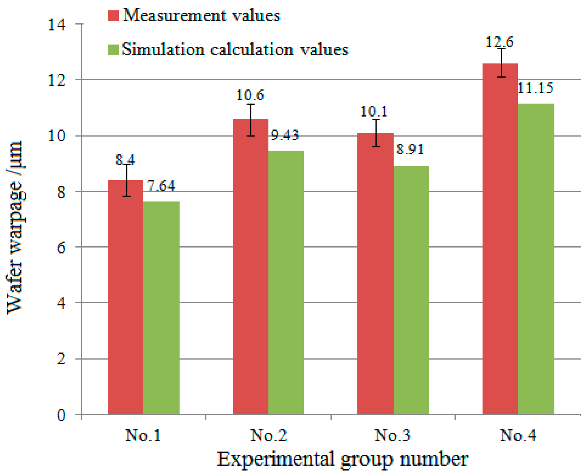
5.2. Experimental Verification of Simulation Calculation Model for Wafer Warpage
5.3. Wafer Warpage under Different Processing Conditions
5.3.1. The Influence of Wafer Thickness on Warpage
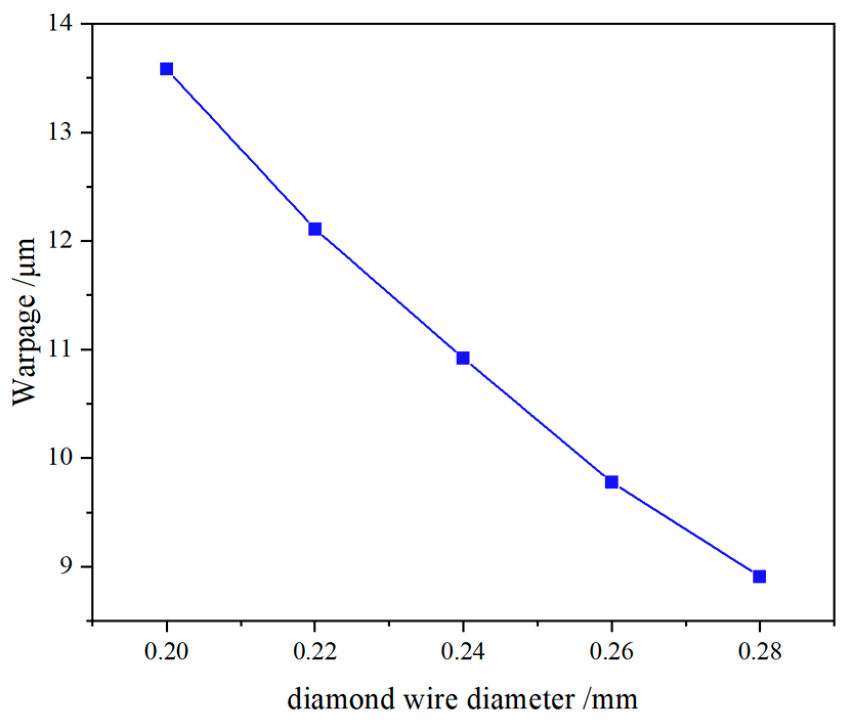
5.3.2. The Influence of Diamond Wire Diameter on Wafer Warpage
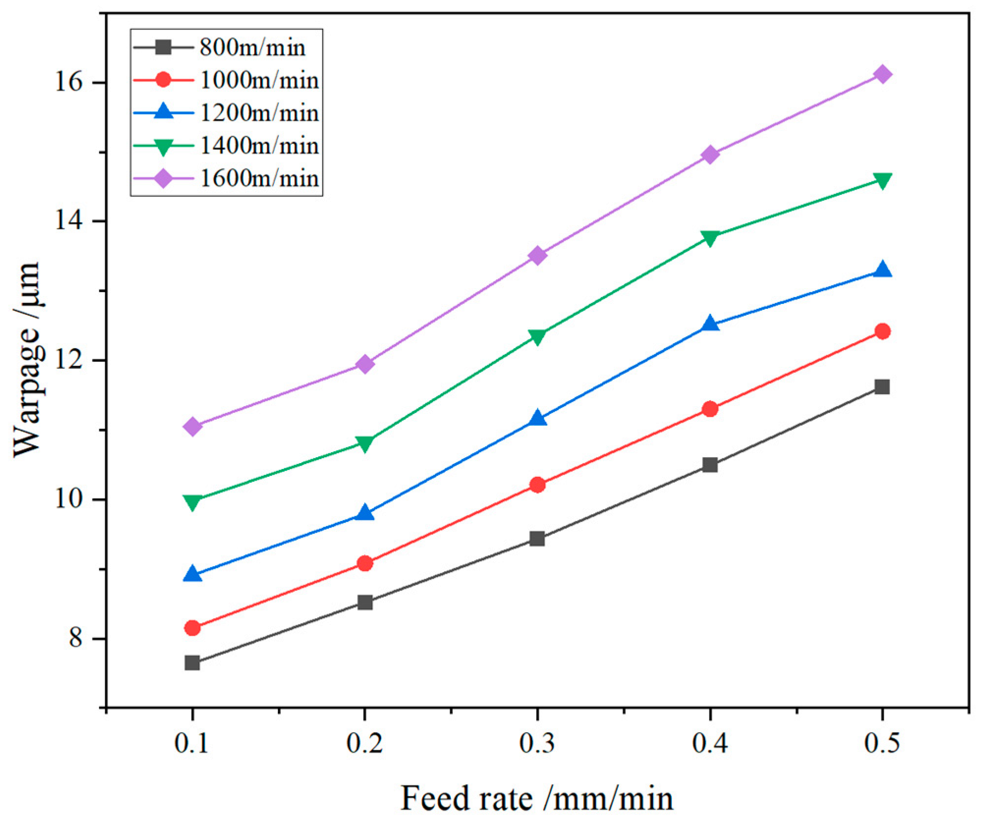
5.3.3. The Influence of Sawing Process Parameters on Wafer Warpage
6. Conclusions
- (1)
- The temperature and deformation at the sawing position is the largest. As the cutting depth increases during sawing, the temperature of the wafer gradually increases and tends to stabilize.
- (2)
- The thickness of sapphire wafers cut by the diamond wire saw decreases, and the smaller the diameter of the diamond wire used, the greater the warpage of the cut wafers.
- (3)
- The sawing process parameters mainly affect the wafer warpage by influencing the heat density and power during sawing. The warpage of sapphire wafers increases with the increase of the saw wire speed and feed rate. How to achieve effective lubrication and cooling of a narrow kerf in sawing processing is the key to obtaining low warpage wafers.
Author Contributions
Funding
Institutional Review Board Statement
Informed Consent Statement
Data Availability Statement
Conflicts of Interest
References
- Xu, Y.; Sun, J.; Zhan, Z.; Fu, B.; Zhan, Y.; Zheng, T. Performance of thermal field-assisted precision lapping for single crystal sapphire wafers. Diam. Abras. Eng. 2023, 43, 649–656. [Google Scholar] [CrossRef]
- Qiu, T.; Jiang, F.; Wang, N.; Lin, J.; Tian, Z.; Wu, Y.; Wen, Q.; Lu, J. Atomistic understanding of the variable nano-hardness of C-plane sapphire considering the crystal anisotropy. J. Mater. Res. Technol. 2024, 29, 4514–4525. [Google Scholar] [CrossRef]
- Liu, Y.; Huang, H.; Wang, L.; Liao, X. Experimental study on normal force of cutting sapphire with multi-wire swing reciprocating wire saw. Diam. Abras. Eng. 2024, 44, 143–150. [Google Scholar] [CrossRef]
- Wang, C.; Ge, P.; He, J.; Wang, X. Influence of crystal anisotropy and process parameters on surface shape deviation of sapphire slicing. Diam. Abras. Eng. 2023, 43, 612–620. [Google Scholar] [CrossRef]
- Yamada, T.; Kinai, F.; Ichikawa, T.; Yokoyama, A.; Fukunaga, M.; Ohshita, T. Warpage analysis of silicon wafer in ingot slicing by wire-saw machine. AIP Conf. Proc. 2004, 712, 1459–1463. [Google Scholar] [CrossRef]
- Gupta, P.; Kulkarni, M. Warp of silicon wafers produced from wire saw slicing: Modeling, simulation, and experiments. ECS Trans. 2006, 2, 123–134. [Google Scholar] [CrossRef]
- Bhagavat, S.; Kao, I. A finite element analysis of temperature variation in silicon wafers during wiresaw slicing. Int. J. Mach. Tools. Manuf. 2008, 48, 95–106. [Google Scholar] [CrossRef]
- Huang, X.; Huang, H.; Guo, H. Simulation and experimental research on the slicing temperature of the sapphire with diamond wire. Int. J. Comput. Methods 2018, 16, 1843003. [Google Scholar] [CrossRef]
- Abe, Y.; Ishikawa, K.; Hitoshi, S. Effects of thermal deformation of multi-wire saw’s wire guides and ingot on slicing accuracy. Key Eng. Mater. 2008, 389–390, 442–447. [Google Scholar] [CrossRef]
- Gao, S.; Dong, Z.; Kang, R.; Zhang, B.; Guo, D. Warping of silicon wafers subjected to back-grinding process. Precis. Eng. 2015, 40, 87–93. [Google Scholar] [CrossRef]
- Drijarkara, A.; Gebrie, T.; Lee, J.; Kang, C. Uncertainty evaluation of thickness and warp of a silicon wafer measured by a spectrally resolved interferometer. Meas. Sci. Technol. 2018, 29, 064009. [Google Scholar] [CrossRef]
- Li, Z.; Liu, X.; Jia, H.; Yu, J.; Cai, Y.; Li, G. Study on the temperature field in the cutting zone for machining monocrystalline silicon wafer using free abrasive multi-wire saw. Mater. Sci. Semicond. Process. 2023, 161, 107481. [Google Scholar] [CrossRef]
- Cheng, D.; Gao, Y.; Liu, R. Finite element analysis on processing stress of polysilicon cut by diamond multi-wire saw. Mater. Sci. Semicond. Process. 2021, 131, 105860. [Google Scholar] [CrossRef]
- Johnsen, L.; Olsen, J.; Bergstrøm, T.; Gastinger, K. Heat Transfer During Multiwire Sawing of Silicon Wafers. J. Thermal Sci. Eng. Appl. 2012, 4, 031006. [Google Scholar] [CrossRef]
- Wang, P.; Ge, P.; Gao, Y.; Bi, W. Prediction of sawing force for single-crystal silicon carbide with fixed abrasive diamond wire saw. Mater. Sci. Semicond. Process. 2017, 63, 25–32. [Google Scholar] [CrossRef]
- Lindholm, D.; Mortensen, D.; Fjær, H.; Yan, S.; Song, A.; Tan, A.; Chua, N. A computer model and methodology to predict temperatures and deformations during diamond multi-wire cutting. AIP Conf. Proc. 2018, 1999, 140002. [Google Scholar] [CrossRef]
- Jiang, D.; Li, L.; Ouyang, S. Handbook of Inorganic Non Metallic Materials; Chemical Industry Press: Beijing, China, 2009. [Google Scholar]
- Jiao, Y.; Ge, P.; Gao, Y.; Bi, W. Analysis of temperature and thermal stress distribution on KDP crystal wire saw slicing. Adv. Mater. Res. 2014, 1027, 28–31. [Google Scholar] [CrossRef]


| Material Parameters | Value | Material Parameters | Value |
|---|---|---|---|
| Density/g·cm−3 | 3.95 | Thermal conductivity/W/(cm·K) | 132.5 |
| Hardness (Moh’s)/GPa | 9 | Fracture toughness/MPa·m1/2 | 2.02 |
| Volume modulus/GPa | 250 | Young modulus/GPa | 320~340 |
| Poisson’s ratio | 0.28 | Thermal expansion coefficient/(×10−6·K−1) | 5.8 |
| No. | Wire Speed Vs (m/min) | Feed Rate Vw (mm/min) |
|---|---|---|
| 1 | 800 | 0.1 |
| 2 | 800 | 0.3 |
| 3 | 1200 | 0.1 |
| 4 | 1200 | 0.3 |
Disclaimer/Publisher’s Note: The statements, opinions and data contained in all publications are solely those of the individual author(s) and contributor(s) and not of MDPI and/or the editor(s). MDPI and/or the editor(s) disclaim responsibility for any injury to people or property resulting from any ideas, methods, instructions or products referred to in the content. |
© 2024 by the authors. Licensee MDPI, Basel, Switzerland. This article is an open access article distributed under the terms and conditions of the Creative Commons Attribution (CC BY) license (https://creativecommons.org/licenses/by/4.0/).
Share and Cite
Liu, Y.; Cheng, D.; Li, G.; Gao, Y. Analysis of Wafer Warpage in Diamond Wire Saw Slicing Sapphire Crystal. Appl. Sci. 2024, 14, 7667. https://doi.org/10.3390/app14177667
Liu Y, Cheng D, Li G, Gao Y. Analysis of Wafer Warpage in Diamond Wire Saw Slicing Sapphire Crystal. Applied Sciences. 2024; 14(17):7667. https://doi.org/10.3390/app14177667
Chicago/Turabian StyleLiu, Yihe, Dameng Cheng, Guanzheng Li, and Yufei Gao. 2024. "Analysis of Wafer Warpage in Diamond Wire Saw Slicing Sapphire Crystal" Applied Sciences 14, no. 17: 7667. https://doi.org/10.3390/app14177667