Abstract
Optoelectronic integrated circuit (OEIC) technology has attracted considerable research attention. Studies have achieved numerous breakthroughs in the basic scientific problems, key technologies, demonstration applications, and industrial promotions of OEIC. This study details the technical process, development status, existing problems, and future research trends of the design, manufacturing, and packaging of OEIC to provide a systematic summary of OEIC technology.
1. Introduction
In 1972, the California Institute of Technology in the United States proposed optoelectronic integration [1]. With the continuous development of technology, optoelectronic integrated circuits are being considered for use in photonic technology and microelectronics technology to integrate photonic devices and electronic devices on the same substrate [2,3,4]. In 1979, Ury and Yariv achieved the monolithic integration of a semiconductor laser and a field-effect transistor (FET) drive device [5]. In 1980, Leheny from Bell Labs realized the monolithic integration of a PIN photodiode and FET [6]. In 1982, Carter et al. achieved the monolithic integration of light-emitting diodes (LEDs), detectors, waveguides, resistors, and FETs in the GaAlAs/GaAs multilayer structure [7]. Since then, optoelectronic integrated circuits have been developed rapidly, and their constituent materials, application processes, and integrated devices have changed frequently, leading to several extensive application fields (Figure 1) of national economic and social development, including network communication, computer, consumer electronics, automotive electronics, transportation, military, and medical industry [2,8,9,10,11,12,13,14,15]. With the increasing trend of optoelectronic integration, optoelectronic integrated circuits have attracted considerable research attention for extending Moore’s law [16,17,18].
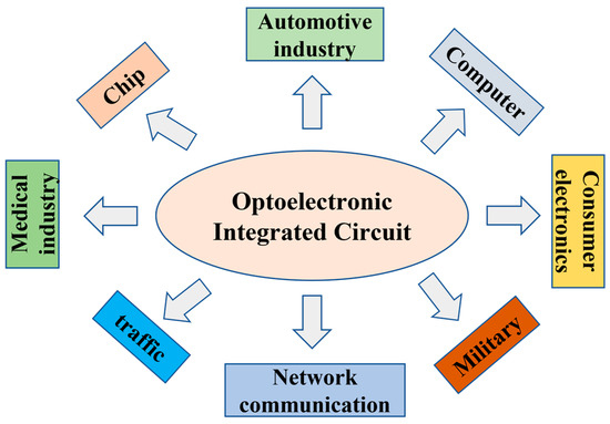
Figure 1.
Application fields of optoelectronic integrated circuits.
Optoelectronic integrated circuit technology is based on optoelectronic technology and microelectronic technology and is used to control optoelectronic integrated circuits, which can control not only the direction of the current within each integrated component, but also the direction of photons to ensure that they flow in a certain direction [19]. Using GaAs, InP, and Si [20,21,22], novel materials and processes have been developed to fabricate light, stable, low-power-consumption, and fast-operation optoelectronic integrated circuits [23]. This study elaborates on the corresponding technological progress from the design, manufacturing, and packaging of the optoelectronic integrated circuit technology chain.
2. Design of Optoelectronic Integrated Circuits
Because the optoelectronic integrated circuit contains optoelectronic devices in addition to the macro-module circuit of the integrated circuit, the circuit transmits not only electrical signals but also optical signals, which render the design of optoelectronic integrated circuits complex, resulting in diversified design indicators and indistinct design levels and complex topology, among others [24]. Therefore, computer-aided software is necessary to help the design of optoelectronic integrated circuits. The design software of optoelectronic integrated circuits is categorized into three classes, namely, chip design aid software, programmable chip design aid software, and system design aid software, including Protel 99SE, PSPICE 17.2, multiSIM10, OrCAD 17.4, PCAD X4.6.2, LSILogic LSI2032, MicroSim V8.0, ISE14.7, and modelsim 2020.4 SE.
Functionally, optoelectronic integrated circuits can be categorized into the following classes: photoelectric conversion, electro-optical conversion, and optical control circuits [25]. Photoelectric conversion converts optical information to electrical information. The optical signal is converted into an electrical signal by a detector and is subsequently processed by amplifiers, consisting of a photodetector, a transistor amplifier, and a bias circuit. Photodetectors require high speed, high sensitivity, high responsiveness, low noise, small capacitance, and easy integration. Studies have focused on the development of transistor amplifiers with high transconductance, high transimpedance, high current gain cut-off frequency, and maximum oscillation frequency. Electro-optical conversion in a circuit converts electrical information to optical information. These circuits consist of an LED, a driving circuit, and a bias circuit. The optical transmitter device is composed of a laser diode (LD), LED, and driving circuit. Studies have focused on the integration of high-rate LD and driver circuits. Optical control circuits consist of guided wave optical circuits, optical isolators, optical modulators, optical switches, optical filters, and other active and passive optical devices connected with intelligent control circuits, such as modulation, amplifier, and temperature field control circuits to guide the optical signal in the optoelectronic integrated circuit for superior integration and interconnection with the optical transmitter module and optical receiver module.
3. Manufacturing of Optoelectronic Integrated Circuits
3.1. Manufacturing Process
Generally, the manufacturing process of optoelectronic integrated circuits is similar to the manufacturing process of integrated circuits and typically includes photomask and mask fabrication, wafer growth, slicing, grinding, oxidation, lithography, etching, diffusion, ion implantation, chemical vapor deposition, and electrode metal vaporization [26]. The following sections detail mask fabrication, imaging, and resistivity control. Mask fabrication through physical vapor deposition, chemical vapor deposition, and vapor phase epitaxy are used to fabricate silicon dioxide, polysilicon, silicon nitride, metal silicide, and metal films. Imaging formation is used in photolithography and etching technology, and the required patterns are formed on various thin-film materials through glue dumping (positive glue and negative glue), exposure, development, etching, and glue removal. Lithography is one of the most critical procedures in the manufacturing process of optoelectronic integrated circuits, requiring a highly technical process, and is one of the neck-locking technologies for optoelectronic integrated circuit manufacturing in China. Etching technology can be categorized into dry etching and wet etching. Of these methods, the wet etching process is simple, exhibits a high etching rate, and has high selectivity. Compared with the conventional wet etching degumming method, the dry etching degumming method exhibits a high etching rate and high reliability. However, because of the high etch rate, even small changes in process parameters can cause large fluctuations in the etch rate. Currently, the resistivity of the material or the local impurity type is typically changed through diffusion and ion implantation to control the resistivity of the material and to facilitate the next step of fabrication.
3.2. Integration Method
According to the integration method (technology), optoelectronic integrated circuits can be categorized into two types, namely, monolithic integration and hybrid integration [27,28]. Monolithic integration is the direct growth of specific materials on substrate materials to integrate multiple optical and electrical components. Hybrid integration involves transferring independent optoelectronic components to the substrate material for interconnection through a certain process. From the comparison in Table 1, monolithic integration and hybrid integration exhibit distinct advantages. Because hybrid integration technology was developed earlier, the process is more mature, and the combination is flexible. Monolithic integration incorporates processes, reduces volume, improves integration, and reduces the effect of component interconnection. Monolithic integration technology exhibits advantages in terms of performance, cost, and mass production and is critical for the development of optoelectronic integration [29].

Table 1.
Comparison of the advantages and disadvantages of monolithic integration and hybrid integration.
Electrical integration technology should focus on the compatibility of manufacturing technology and the cross-integration with other disciplines. Existing optoelectronic integrated materials include lithium niobate (LiNbO3), silicon-on-insulator (Si), silicon dioxide (SiO2), silicon nitride (Si3N4), optical glass, polymers, and III–V semiconductor materials [30,31], which exhibit distinct properties (Table 2). Lithium niobate exhibits excellent electro-optical modulation properties, polymeric materials require simple processing, and silicon materials allow for large-scale integration. For the development of optoelectronic integrated circuits, various materials should be devised to complete the system integration. In 2017, Datta et al. [32] replaced the conventional optoelectronic integrated materials with materials mixed with graphene and silicon nitride and produced optoelectronic modulators with enhanced optical models, superior modulation efficiency, and considerably reduced functional consumption. Regardless of the materials in optoelectronic integrated circuits, they exhibit optical loss when integrated on a large scale. Therefore, in the future, the development of optoelectronic integrated circuits should focus on reducing the energy consumption required for optical transmission.
Table 2.
Comparison of the advantages and disadvantages of matrix materials for OEIC.
3.2.1. Monolithic Integration
Since Ury and Yariv realized monolithic integration in 1979 [5], monolithic integration has continued. Currently, monolithic integration solutions are heterogeneous epitaxial lasers on Si materials or III–V materials, and the integration processes are typically Butt-joint regrowth technology, bias quantum well technology, and quantum well mixing technology [32,33,34,35,36,37,38]. Among them, silicon-based monolithic integration incorporates Si CMOS manufacturing technology on the same silicon wafer to integrate multiple components for realizing the transmission and processing of multiple optical signals on the same chip. InP-based monolithic integration technology is mature. The energy band structure of quantum wells is changed on InP material substrates through quantum well mixing technology, docking growth technology, same active region method, and selected region epitaxy technology to realize the integration of optoelectronic components with various functions. In 1989, Kouping invented a monolithic integrated transceiver for III–V devices on silicon wafers through selective metal–organic chemical vapor deposition (MOCVD) on silicon substrates. The technology grows compound semiconductor materials, obtains high-quality GaAs epitaxial structures on Si substrates, and gradually fabricates light emitters and light receivers on the deposited epitaxial layers, realizing a Si-based monolithic integrated optical transceiver chip [39]. In 1997, Soref Richard et al. invented a laser array, with each laser having a SiGe-graded relaxation buffer layer and a highly doped stable strained SiGe or Ge collector layer grown sequentially on a Si wafer and emitted by SiGe. Extremely covered symmetric Ge–Si superlattices with many thin 8–15 atom monolayers of interleaved Ge and Si atoms enable high stacking heights [40]. Amber wave systems disclosed structures with optically active layers embedded in Si wafers such that the outermost epitaxial layer exposed to CMOS processing equipment is always Si or other CMOS-compatible material (SOI or SiO2), and optical signals can be transmitted between the embedded optoelectronic layer and the external waveguide using normal incidence (through the Si substrate or top Si cap layer) or in-plane incidence (edge coupling) [41]. Lestra announced a transceiver with a light pipe with an inclined reflective surface that generates a first light signal in the chip based on the light source signal, transmits the first light signal from the chip through the light pipe, receives the second light signal from the light pipe, and converts the second light signal through the electrical signal of the photodetector [42]. Huazhong University of Science and Technology used quantum well mixing technology to achieve on-chip photonic integration of passive and active optoelectronic devices. They subsequently prepared InP-based monolithic integrated optical phased arrays [43]. The U.S. Naval Laboratory provided building blocks for on-chip chemical sensors and other highly compact photonic integrated circuits that combine interband or quantum cascade lasers and detectors with passive waveguides integrated into III–V or other components on Si [44]. In 2019, Acacia Communications Co., Ltd., proposed a structure and the fabrication method of a monolithic Si coherent transceiver with integrated lasers and gain elements in which an InP chip was bonded to a Si chip in a notch formed in the Si chip [45]. Junbo Feng et al. [46] used Si-based CMOS technology to monolithically integrate Si-based optoelectronic modulators and a quadrature hybrid coupler to produce a monolithic integrated sideband modulator with a high sideband rejection ratio, simple driving, and large operating bandwidth. With the continuous development of monolithic integration technology, smaller size, lower power consumption, and lower cost are primary development directions. However, in submicron-scale etching technology, the connection between photonic and electronic devices, process compatibility, thermal isolation and electrical isolation, the integration of light sources, optical transmission loss and coupling efficiency, and optical logic devices remain challenging.
3.2.2. Hybrid Integration
Hybrid integration is the most widely studied optoelectronic integration technology in which optoelectronic components are integrated with various functions on the substrate material through direct placement or a bonding process [47,48,49,50]. Among them, the direct placement involves using flip-chip bonding or mounting process, placing the pre-fabricated III–V material laser on the surface of the Si photonic chip, and completing the electrical connection through solder balls to realize the hybrid integration of the light source and the Si optical waveguide device [51]. Tanaka et al. designed a silicon photonic transmitter chip without temperature control by integrating a III–V material semiconductor optical amplifier (SOA) on an SOI material substrate using flip-chip technology [52]. Flip-chip welding technology renders the design of Si optical components and SOA flexible and improves SOA thermal conductivity. End-face coupling requires flip-chip welding with a high degree of accuracy. The flip-chip welding technology is mature and can also be used effectively because of the optical gain characteristics of III–V materials. However, the high alignment accuracy requirements result in higher process costs. Bonding involves integrating the III–V material epitaxial layer with Si optical components. Because of the high alignment tolerance of the bonding process, compared with the direct placement process, this method exhibits a superior alignment accuracy advantage [29]. The bonding process is categorized into direct bonding and adhesive bonding. Direct bonding involves directly contacting two smooth, flat, and clean wafers without using bonding materials. Lasky and Shimbo et al. [53,54] proposed forming a bond between the two wafers under the action of the interface bond. Adhesive bonding integrates inter-wafer bonding using specific bonding materials. Benzocyclic (BCB) as a binder is mature, and BCB exhibits a strong bonding effect with excellent flatness and thermal stability. Compared with direct bonding, the thermal conductivity of the BCB material is poor, which results in poor heat dissipation of the integrated device and reduces light source performances. The “cold bonding” process proposed by Keyvaninia et al. [55] is similar to the developed mainstream “low temperature bonding” principle and can effectively address the aforementioned problems. The room-temperature bonding process should be used for future bonding technology development [56]. Ke et al. [57] developed a high-speed integrated tunable optical delay line using a novel preparation method. The substrate material of this delay line is silicon material, and the waveguide material is silicon nitride optical waveguide and lithium niobate optical waveguide. The lithium oxide material is a thin-film material, and the adopted BCB-based bonding process renders the process flexible and does not require a chemical mechanical polishing process. In 2019, Li et al. [58] used a hybrid integration scheme in which the chip and circuit were bonded by a gold wire to prepare a high-gain four-channel miniaturized optical receiver module device, which reduces the size and power consumption of the communication system and has numerous application areas.
3.3. Optical Interconnect
With the increasing demand and miniaturization of transistors, the data transmission between chips and within chips requires higher bandwidth and speed and lower power consumption. Optical interconnects with low power consumption and interference have numerous advantages [59]. In the future, optoelectronic integrated circuits will replace conventional electrical interconnects with optical interconnects. Studies have focused on optical interconnect [60,61,62,63]. In 1982, Fujitsu devised a silicon-based waveguide to simplify the device structure and reduce the device size and cost [64]. In 1984, Goodman et al. [65] proposed to replace conventional electrical interconnection with optical interconnection technology. In 1987, Richard Soref et al. [66] proposed an optical waveguide based on the SOI platform. The SOI material exhibits excellent core-cladding refractive index difference and mitigates loss. Subsequently, this method was used to develop silicon-based waveguides. In 1993, Berger et al. [67] prepared porous Si optical waveguides by varying the current intensity in the electrochemical etching process used to fabricate porous Si, which affects the porosity of the monolayer and the optical properties in a simple manner. In 2004, Sun Yat-Sen University [68] proposed an integrated optical waveguide device based on the principle of multi-mode interference, with a structural unit of 3 × 2 for optical power separation and optical cross-interconnection. By introducing the MMI region near the crossover point, the crosstalk characteristics of the crossover waveguide improved considerably. In 2015, IBM [69] used the effect of grain size on optical loss to propose a low-loss large-grain polysilicon waveguide with a high refractive index to integrate various small photonic components. Furthermore, the use of small optical components improves performance. In 2018, the University of Arizona [70] introduced a waveguide that includes a thin waveguide core and a tapered structure design that provides previously unachievable performance, including efficient coupling with considerably reduced footprint, loose alignment tolerances, and low polarization dependence. These features are critical for high-volume manufacturing using low-cost, low-accuracy assembly tools. Generally, the optical interconnection system consists of light sources, electro-optic modulators, optical waveguides, optical switches, filters, wavelength division multiplexing, and optical detectors. The interconnection process includes the light emitted by the light source being used as a data transmission carrier. The electro-optic modulator loads the electrical signal to be transmitted on the optical carrier, transmits it to the interconnection terminal through the optical waveguide, and, finally, receives and demodulates it into an electrical signal via the detector [71,72]. Structurally, optical interconnects include intra-chip interconnects, inter-chip interconnects, inter-module interconnects, inter-board interconnects, and interconnects between communication devices [39]. The optical interconnection technology is mature and has been commercialized. The optical interconnection technology between circuit boards, modules, and chips is developing, whereas the optical interconnection within the chip is in the application basic research stage, and the optical interconnection technology is accelerating to in-chip development. From the transmission channel, optical interconnection includes free space interconnection, waveguide interconnection, and optical fiber interconnection. Among them, free space interconnection exhibits optical path alignment, and waveguide interconnection provides high-density interconnection channels, which are suitable for interconnection within chips or between chips. They are crucial in optoelectronic integrated circuits and are a current research focus in optical interconnection. The chip-level optical interconnection technology of optical waveguides is typically focused on the improvement of the waveguide and the improvement of the fabrication process.
4. Packaging of Optoelectronic Integrated Circuits
The packaging of optoelectronic integrated circuits is the system integration of optoelectronic devices, electronic components, and functional application materials [73]. With the continuous development of optoelectronic integrated circuit technology, requirements for transmission speed, performance index, form factor, and packaging cost in terms of packaging have become stringent. Thus, promoting the progress and innovation of packaging technology is essential for the packaging technology to experience double-inline insertion, butterfly packaging, coaxial packaging, Mini-DL packaging, small form factor packaging, chip on board (COB), tape automated bonding (TAB), and flip-chip (FC) [74,75]. Based on the packaging form, packaging can be categorized into monolithic packaging and optoelectronic co-package (photoelectric hybrid packaging). Among these, optoelectronic co-packaging is a mixing package of microelectronic technology and photonic technology, which can not only give full play to the advantages of fast optical interconnection speed, large bandwidth, anti-interference, high density, and low power consumption, but also use the mature microelectronics technology, high-density integration, high yield, low cost, and other advantages, which is a critical topic of research.
4.1. Monolithic Package
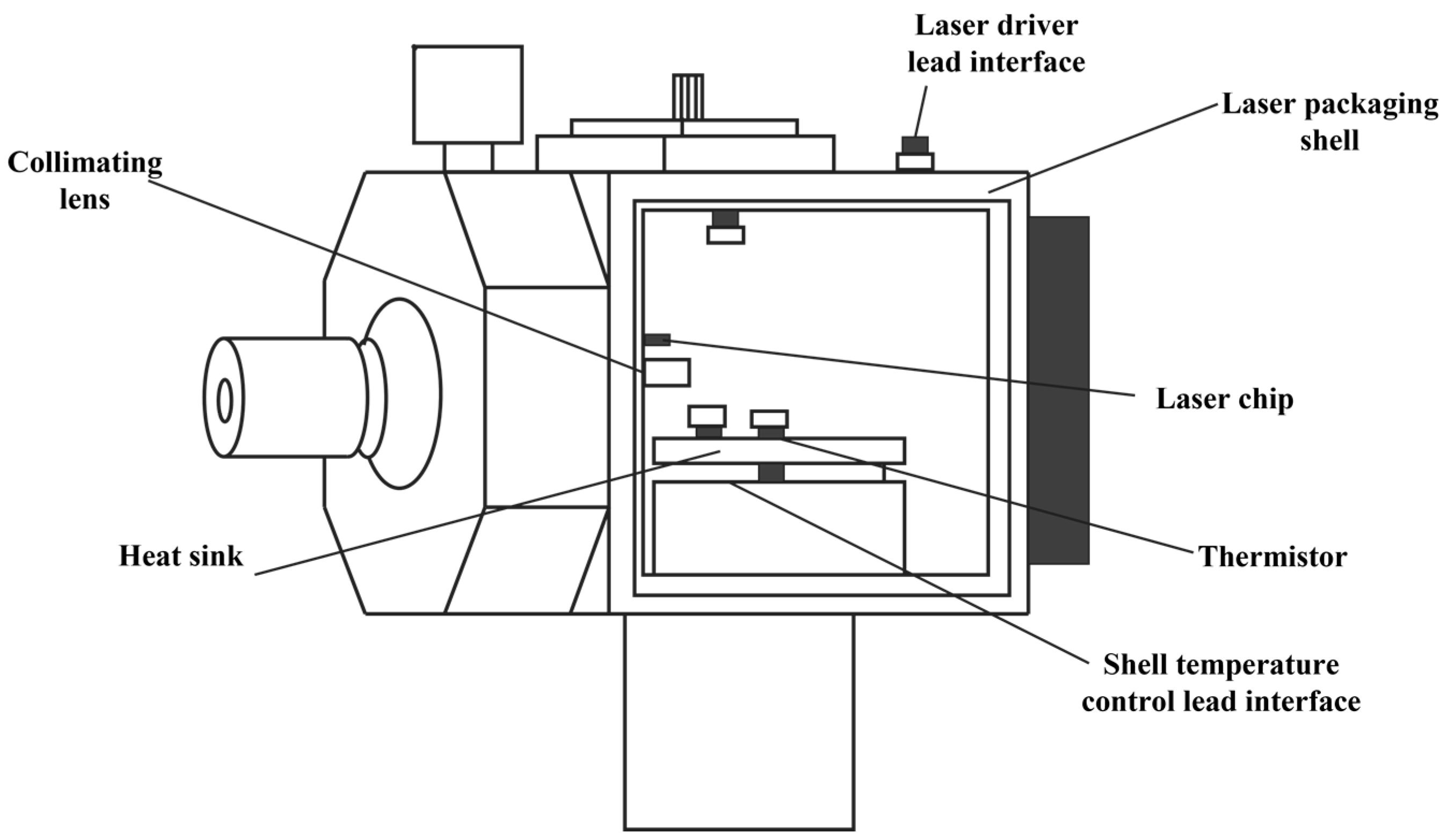
Monolithic packaging is the packaging of monolithic integration formed by the simultaneous processing of optical and electrical devices on the same tape-out platform [76]. With the continued demand for smaller and superior optoelectronic integrated circuit devices causing manufacturers to increase component density and reduce component size wherever possible within the device, the development of package structures should be on the chip level, wafer level, and even quantum level to achieve minimal package occupancy area. In 1983, Eales et al. [77] of STC Company detailed a package scheme, based on a ceramic substrate. The heat sink is electrically connected to the top of the laser by wire bonding technology. In 1995, the Korea Institute of Electronics and Communications disclosed a butterfly packaging scheme [78], which can transmit high-speed signals to the micro pin lines of package pins installed on the micro pin lines and the front surface of the feedback optical interrupter, and fixed them through laser welding to minimize the optical fiber in heat transfer path to improve the reliability of module packaging. In 2005, Taiwan Semiconductor Manufacturing Company revealed a packaging structure for optical elements [79]. The chip has optical components and a plurality of pads arranged on its active surface; holes are formed through the chip and electrically connected with the pads. The cover is attached to the active surface through an adhesive ring, and a plurality of metal wires are arranged on the rear surface of the chip. This packaging structure can be used for wafer-level mass manufacturing, which not only reduces the packaging cost considerably but also improves the reliability of packaging. In 2016, Ma et al. [80] invented a monolithic packaging scheme to prepare an insulating film on the microchannel cooler to achieve water–electric separation, which can reduce the requirement for cooling water resistivity and incorporate the use of ordinary cooling water, which is conducive for improving the environmental adaptability of the laser and extending the lifetime of the laser. In 2018, Shi Zhe et al. invented a package structure design scheme for quantum cascade lasers [81], as depicted in Figure 2, which not only improves the collimated coupling efficiency and the flexibility of replacing the laser chip but also reduces the package cost and assembly difficulty and reduces the package volume. Monolithic packaging schemes are increasingly prioritizing higher reliability and smaller size, which are simple for monolithic packaging technology but also lead to a higher loss of optical waveguide and a lower response rate of photoelectric conversion, which results in the optoelectronic device becoming unable to perform optimally [82].

Figure 2.
Schematic of the quantum cascade laser packaging structure.
4.2. Optical Co-Package
Optical co-packaging encapsulates optical transceiver modules/chips and integrated circuit chips in one package [83]. The packaging structure is divided into 2D, 2.5D, and 3D packaging (Figure 3). The packaging process includes COB, TAB, and FC. Furthermore, 2D packaging is typically directly interconnected by wire bonding, which is realized through COB packaging technology. The COB packaging process is a packaging technology in which the chip is directly bound to the PCB board or metal-based printed circuit board through a COB solid-state machine, and the chip and the circuit board are electrically connected through wire bonding. Dozens or even hundreds of chips are packaged in the area. In 1987, Siemens disclosed a hybrid packaging structure for electro-optical components [84], which was the earliest patent involving hybrid packaging, using a 2D packaging structure to achieve a high-precision and correct assembly of optoelectronic component circuits in a metal housing containing optical components without the use of gluing and brazing. Although the assembly of 2D packaging is easy, the high-speed signal interconnection of optical and electrical devices is long, and the occupied area is relatively large, which considerably reduces the integration density and bandwidth. Here, 2.5D packaging includes co-packaging the optical transceiver module and the integrated circuit chip on a carrier board, with higher interconnection density and lower power consumption. In 1995, Canon Japan disclosed an optoelectronic hybrid packaging method using a TAB packaging process and 2.5D packaging structure [85], which can be applied to produce various types of equipment, suitable for mass production, low manufacturing cost, and easy-to-solder chips to the circuit board. TAB involves mounting and connecting the integrated circuit chip on a soft, film-like polymer carrier tape and automatically soldering the inner lead end of the carrier tape to the chip integrated circuit, whereas the outer lead end is connected to the conventional package or printed board PWB soldering, a highly automated surface mount technology, and provides numerous terminal interconnects, typically used for mass production greater than 500 pieces. In 2002, the Industrial Technology Research Institute of Taiwan, a consortium, disclosed a packaging method for optoelectronic components using a 2.5D packaging structure [86], consisting of an optical transceiver package, a driver circuit bonding, a microlens bonding package, and a plug-in connector, which enables the effective alignment of optical transceivers, reduces costs, improves yields, and is suitable for high-volume production. In 2014, China’s Huajin Semiconductor revealed an optical component packaging method using a 2.5D package combined with a stop-hole packaging method for optical communication devices [87], which can reduce the temperature of VCSEL arrays under normal operation by approximately 20 °C while maintaining a smaller size and lower manufacturing cost and can reduce space while directly coupling optical fibers and optoelectronic devices. In 2020, Infineon from Germany developed a semiconductor packaging method using the FC packaging process [88], which provides semiconductor packaging technology with component stacking arrangement that allows components to communicate over very short distances, reducing parasitic inductance, for applications requiring low-inductance electrical connections between package components, such as LIDAR systems and power semiconductor modules. Next, 3D packaging is a three-dimensional stacking of integrated circuit chips and optical chips to achieve the shortest electrical interconnection with low losses, the highest interconnection density, and lower power consumption than the 2.5D solution. Compared with 2D packaging methods, 2.5D and 3D packages incorporate the use of three-dimensional interconnects to allow spatial wiring in a 3D manner and improve integration, which reduces the length of on-chip connectivity, improves transmission speed, and reduces power consumption, providing a superior system integration solution for miniaturization, low power consumption, and broadband interconnect requirements. With the continuous development and maturation of packaging technology, package integration has evolved from 2.5D to 3D optoelectronic co-packaging [83]. Among many packaging processes, FC is both a chip interconnection technology and an ideal chip bonding technology, and FC has become the preferred packaging process in the packaging field.
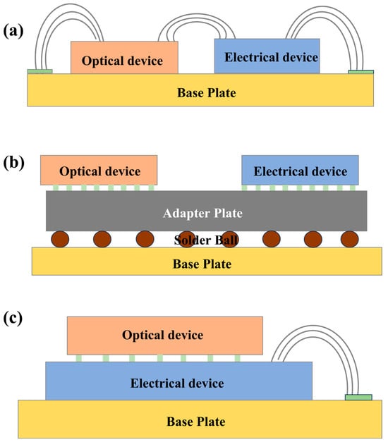
Figure 3.
Schematic of (a) 2D, (b) 2.5D, and (c) 3D package structure.
5. Summary and Outlook
With the wide applications of the semiconductor industry in various fields and the continuous development of the integration process, optoelectronic integrated circuits will attract considerable research attention. Currently, for the field of optoelectronic integration, studies should focus on continuously optimizing the optoelectronic integration process, improving the efficiency of large-scale optoelectronic integration, and reducing the cost of preparation materials and the preparation process to realize low-cost preparation and mass production on a large scale. In the preparation process, monolithic integration gradually exhibits excellent performance, which is a critical topic of research in optoelectronic integrated circuits. The research on optical interconnect technology is typically focused on the modification of the optical waveguide and the preparation process. The optical waveguide and preparation process typically focus on reducing cost and loss and improving the transmission rate. Improved efficacy, reduction of cost and losses, and enhanced transmission rates are typically achieved through improvements in optical waveguides and fabrication processes. Along with the development of packaging technology, optoelectronic co-packaging can not only improve the interconnection density, but also reduce the size and weight of optoelectronic integrated circuits and reduce power consumption.
Author Contributions
Conceptualization, M.L. and Y.C.; methodology, X.L.; validation, L.P.; formal analysis, C.Z.; resources, D.C.; writing—original draft preparation, M.L., D.C. and L.C.; writing—review and editing, M.L. and J.F.; supervision, J.F.; funding acquisition, X.L. All authors have read and agreed to the published version of the manuscript.
Funding
This research received no external funding.
Institutional Review Board Statement
Not applicable.
Informed Consent Statement
Not applicable.
Data Availability Statement
Not applicable.
Acknowledgments
This research was funded by the Patent Special Research Project of China National Intellectual Property Administration in 2021 [Grant number fx202102], and the project commissioned by the company COFCO (Jilin) Bio-Chemical Technology Co., Ltd.
Conflicts of Interest
The authors declare no conflicts of interest.
References
- Garmire, E.; Stoll, H.; Yariv, A.; Hunsperger, R.G. Optical waveguiding in proton-implanted GaAs. Appl. Phys. Lett. 1972, 21, 87–88. [Google Scholar] [CrossRef]
- Sengupta, K.; Nagatsuma, T.; Mittleman, D.M. Terahertz integrated electronic and hybrid electronic–photonic systems. Nat. Electron. 2018, 1, 622–635. [Google Scholar] [CrossRef]
- Hao, Y.; Xiang, S.; Han, G.; Zhang, J.; Ma, X.; Zhu, Z.; Guo, X.; Zhang, Y.; Han, Y.; Song, Z.; et al. Recent progress of integrated circuits and optoelectronic chips. Sci. China Inf. Sci. 2021, 64, 1–33. [Google Scholar] [CrossRef]
- Ali, J.; Youplao, P.; Pornsuwancharoen, N.; Chaiwong, K.; Chiangga, S.; Amiri, I.; Punthawanunt, S.; Singh, G.; Yupapin, P.; Grattan, K. An integrated microring circuit design for optoelectronic transformer applications. Results Phys. 2018, 11, 706–708. [Google Scholar] [CrossRef]
- Ury, I.; Margalit, S.; Yust, M.; Yariv, A. Monolithic integration of an injection laser and a metal semiconductor field effect transistor. Appl. Phys. Lett. 1979, 34, 430–431. [Google Scholar] [CrossRef]
- Leheny, R.F.; Nahory, R.E.; Pollack, M.A.; Ballman, A.A.; Beebe, E.D.; DeWinter, J.C.; Martin, R.J. Integrated In0.53Ga0.47As p-i-n f.e.t. Photoreceiver; Electronics Letters; Institution of Engineering and Technology: Stevenage, UK, 1980; pp. 353–355. [Google Scholar]
- Carter, A.; Forbes, N.; Goodfellow, R. Monolithic integration of optoelectronic, electronic and passive components in GaAlAs/GaAs multilayers. Electron. Lett. 1982, 18, 72–74. [Google Scholar] [CrossRef]
- Essebe, D.E.; Mengue, A.D.; Essimbi, B.Z. Simulink implementation of a new optoelectronic integrated circuit: Stability analysis and infinite-scroll attractor. Opt. Quantum Electron. 2021, 53, 388. [Google Scholar] [CrossRef]
- Yi, L.; Kaname, R.; Nishida, Y.; Yu, X.; Fujita, M.; Nagatsuma, T. Imaging Applications with a Single Resonant Tunneling Diode Transceiver in 300-GHz Band. In Proceedings of the 2020 International Topical Meeting on Microwave Photonics (MWP), Virtual, 24–26 November 2020; pp. 120–123. [Google Scholar]
- Okamoto, K.; Tsuruda, K.; Diebold, S.; Hisatake, S.; Fujita, M.; Nagatsuma, T. Terahertz Sensor Using Photonic Crystal Cavity and Resonant Tunneling Diodes. J. Infrared Millim. Terahertz Waves 2017, 38, 1085–1097. [Google Scholar] [CrossRef]
- Yu, X.; Kim, J.-Y.; Fujita, M.; Nagatsuma, T. Efficient mode converter to deep-subwavelength region with photonic-crystal waveguide platform for terahertz applications. Opt. Express 2019, 27, 28707–28721. [Google Scholar] [CrossRef]
- Stake, J.; Malko, A.; Bryllert, T.; Vukusic, J. Status and Prospects of High-Power Heterostructure Barrier Varactor Frequency Multipliers. Proc. IEEE 2017, 105, 1008–1019. [Google Scholar] [CrossRef]
- Huang, C.-Y.; Chen, K.-C.; Chang, C.-J. Realization of a self-powered ZnSnO MSM UV photodetector that uses surface state controlled photovoltaic effect. Ceram. Int. 2021, 47, 1785–1791. [Google Scholar] [CrossRef]
- Guo, Y.; Li, Y.; Zhang, Q.; Wang, H. Self-powered multifunctional UV and IR photodetector as an artificial electronic eye. J. Mater. Chem. C 2017, 5, 1436–1442. [Google Scholar] [CrossRef]
- Mishra, M.; Gundimeda, A.; Garg, T.; Dash, A.; Das, S.; Vandana; Gupta, G. ZnO/GaN heterojunction based self-powered photodetectors: Influence of interfacial states on UV sensing. Appl. Surf. Sci. 2019, 478, 1081–1089. [Google Scholar] [CrossRef]
- Tassin, P.; Koschny, T.; Soukoulis, C.M. Graphene for Terahertz Applications. Science 2013, 341, 620–621. [Google Scholar] [CrossRef] [PubMed]
- Liu, Y.; Wang, S.; Liu, H.; Peng, L.-M. Carbon nanotube-based three-dimensional monolithic optoelectronic integrated system. Nat. Commun. 2017, 8, 15649. [Google Scholar] [CrossRef]
- Capmany, J.; Gasulla, I.; Pérez, D. The programmable processor. Nat. Photonics 2016, 10, 6–8. [Google Scholar] [CrossRef]
- Tan, M.; Ming, D.; Wang, Z.C. From photonic integration to electronic-photonic heterogeneously-converging integrated circuits: A case study of wavelength locking of microrings. Micro/Nano Electron. Intell. Manuf. 2019, 1, 40. [Google Scholar]
- Song, W.; Wang, X.; Chen, H.; Guo, D.; Qi, M.; Wang, H.; Luo, X.; Luo, X.; Li, G.; Li, S. High-performance self-powered UV-Vis-NIR photodetectors based on horizontally aligned GaN microwire array/Si heterojunctions. J. Mater. Chem. C 2017, 5, 11551–11558. [Google Scholar] [CrossRef]
- Meng, J.; Qi, L.; Liu, X.; Zhou, J.; Zhang, D.; Jin, Z. The Design of Terahertz Monolithic Integrated Frequency Multipliers Based on Gallium Arsenide Material. Micromachines 2020, 11, 336. [Google Scholar] [CrossRef]
- Hussain, K.; Shuja, A.; Ali, M.; Fahad, S. Carrier removal and transport in photonic integrated circuit ready InGaAsP/InP substrate: Electrical and transients of charges evaluation. Mater. Sci. Semicond. Process. 2020, 121, 105384. [Google Scholar] [CrossRef]
- Chen, S.; Shi, Y.; He, S.; Dai, D. Low-loss and broadband 2 × 2 silicon thermo-optic Mach-Zehnder switch with bent directional couplers. Opt. Lett. 2016, 41, 836–839. [Google Scholar] [CrossRef]
- Duan, L.; He, F.; Tian, Y.; Sun, B.; Fan, J.; Yu, X.; Ni, L.; Zhang, Y.; Chen, Y.; Zhang, W. Fabrication of Self-Powered Fast-Response Ultraviolet Photodetectors Based on Graphene/ZnO:Al Nanorod-Array-Film Structure with Stable Schottky Barrier. ACS Appl. Mater. Interfaces 2017, 9, 8161–8168. [Google Scholar] [CrossRef] [PubMed]
- Cai, X.; Wang, S.; Peng, L.-M. Recent progress of photodetector based on carbon nanotube film and application in optoelectronic integration. Nano Res. Energy 2023, 2, e9120058. [Google Scholar] [CrossRef]
- Panchenko, E.; Cadusch, J.J.; Avayu, O.; Ellenbogen, T.; James, T.D.; Gómez, D.; Roberts, A. In-Plane Detection of Guided Surface Plasmons for High-Speed Optoelectronic Integrated Circuits. Adv. Mater. Technol. 2018, 3, 1700196. [Google Scholar] [CrossRef]
- Xu, K. Silicon electro-optic micro-modulator fabricated in standard CMOS technology as components for all silicon monolithic integrated optoelectronic systems. J. Micromechanics Microengineering 2021, 31, 054001. [Google Scholar] [CrossRef]
- Liu, Y.; Zhang, J.; Peng, L.-M. Three-dimensional integration of plasmonics and nanoelectronics. Nat. Electron. 2018, 1, 644–651. [Google Scholar] [CrossRef]
- Huang, B.; Zhang, Z.; Zhang, Z. Research progress on monolithic integration of silicon based optoelectronics with microelectronics. Micro/Nano Electron. Intell. Manuf. 2019, 1, 55–67. [Google Scholar]
- Chen, J.; Ouyang, W.; Yang, W.; He, J.; Fang, X. Recent Progress of Heterojunction Ultraviolet Photodetectors: Materials, Integrations, and Applications. Adv. Funct. Mater. 2020, 30, 1909909. [Google Scholar] [CrossRef]
- Zimmermann, H. Silicon Optoelectronic Integrated Circuits; Springer: Berlin/Heidelberg, Germany, 2018. [Google Scholar]
- Datta, I.; Phare, C.T.; Dutt, A.; Mohanty, A.; Lipson, M. Integrated Graphene Electro-Optic Phase Modulator. In Proceedings of the Conference on Lasers and Electro-Optics, Optica Publishing Group, San Jose, CA, USA, 14–19 May 2017; p. STu3N.5. [Google Scholar]
- Fang, Y.-Q.; Luo, K.; Gao, X.-G.; Huo, G.-Q.; Zhong, A.; Liao, P.-F.; Pu, P.; Bao, X.-H.; Chen, Y.-A.; Zhang, J.; et al. High detection efficiency silicon single-photon detector with a monolithic integrated circuit of active quenching and active reset. Rev. Sci. Instrum. 2020, 91, 123106. [Google Scholar] [CrossRef]
- Kim, C.; Koyama, A.; Shimazoe, K.; Takahashi, H.; Takeshita, T.; Kurachi, I.; Miyoshi, T.; Nakamura, I.; Kishimoto, S.; Arai, Y. Development of circuit integrated monolithic SOI-SiPM for radiation detection. J. Instrum. 2020, 15, C02049. [Google Scholar] [CrossRef]
- Schulz, W.-M.; Spang, M.; Wintrich, A.; Konig, B.; Berberich, S.E. Novel Monolithic Integrated Device with Gate Resistor for External IGBT Clamping Leading to Enhanced Short Circuit Behavior. In Proceedings of the 2021 33rd International Symposium on Power Semiconductor Devices and ICs (ISPSD), Virtual, 30 May–3 June 2021. [Google Scholar]
- Shen, G.; Che, W.; Feng, W.; Shi, Y.; Shen, Y.; Xu, F. A Miniaturized Ka-Band Bandpass Filter Using Folded Hybrid Resonators Based on Monolithic Microwave Integrated Circuit Technology. IEEE Trans. Circuits Syst. II Express Briefs 2021, 68, 1778–1782. [Google Scholar] [CrossRef]
- Zhang, L.; Tong, X.; Han, J.; Cheng, X. A 45–61 GHz monolithic microwave integrated circuit subharmonic mixer incorporating dual-band power divider. Microw. Opt. Technol. Lett. 2020, 62, 2851–2856. [Google Scholar] [CrossRef]
- Cheng, C.; Huang, B.; Mao, X.; Zhang, Z.; Zhang, Z.; Geng, Z.; Xue, P.; Chen, H. Monolithic optoelectronic integrated broadband optical receiver with graphene photodetectors. Nanophotonics 2017, 6, 1343–1352. [Google Scholar] [CrossRef]
- Zavracky, P.M.; Zavracky, M.M.; Fan, J.C.; Salerno, J.P. Monolithic Integrated Transceiver of III–V Devices on Silicon. U.S. Patent 4,989,934, 5 February 1991. [Google Scholar]
- Soref, R.A.; Friedman, L.R. Silicon-Based Strain-Symmetrized Ge-Si Quantum Lasers. U.S. Patent 6,154,475, 28 November 2000. [Google Scholar]
- Ting, S.; Bulsara, M.T.; Yang, V.; Groenert, M.; Samavedam, S.; Currie, M.; Langdo, T.; Fitzgerald, E.A.; Joshi, A.M.; Brown, R.; et al. Monolithic integration of III-V materials and devices on silicon. In Proceedings of the Optoelectronics 9‘9—Integrated Optoelectronic Devices, San Jose, CA, USA, 23–29 January 1999. [Google Scholar]
- de Dobbelaere, P. Integrated Transceiver with Lightpipe Coupler. U.S. Patent 7773836, 10 August 2010. [Google Scholar]
- Joo, J.; Jang, K.-S.; Kim, S.H.; Kim, I.G.; Oh, J.H.; Kim, S.A.; Kim, G.; Jeong, G.-S.; Chi, H.; Jeong, D.-K. 100 Gb/s photoreceiver module based on 4ch × 25 Gb/s vertical-illumination-type Ge-on-Si photodetectors and amplifier circuits. In Silicon Photonics XI; SPIE: Bellingham, WA, USA, 2016. [Google Scholar]
- Wang, R.; Vasiliev, A.; Muneeb, M.; Malik, A.; Sprengel, S.; Boehm, G.; Amann, M.-C.; Šimonytė, I.; Vizbaras, A.; Vizbaras, K.; et al. III–V-on-silicon photonic integrated circuits for spectroscopic sensing in the 2–4 μm wavelength range. Sensors 2017, 17, 1788. [Google Scholar] [CrossRef]
- Doerr, C.; Chen, L. Monolithic Silicon Coherent Transceiver with Integrated Laser and Gain Elements. U.S. Patent 10284300B2, 7 May 2019. [Google Scholar]
- Falconi, F.; Porzi, C.; Melo, S.; Nottola, A.; Tirelli, S.; Preve, G.B.; Sorel, M.; Bogoni, A. Wideband single-sideband suppressed-carrier modulation with silicon photonics optical filters. In Proceedings of the 2019 International Topical Meeting on Microwave Photonics (MWP), Ottawa, ON, Canada, 7–10 October 2019; pp. 1–4. [Google Scholar]
- Slight, T.J.; Romeira, B.; Wang, L.; Figueiredo, J.M.L.; Wasige, E.; Ironside, C.N. A LiÉnard Oscillator Resonant Tunnelling Diode-Laser Diode Hybrid Integrated Circuit: Model and Experiment. IEEE J. Quantum Electron. 2008, 44, 1158–1163. [Google Scholar] [CrossRef]
- Zhao, H.; Zhang, Y.; Zhang, K.; Huang, J.; Ran, H. Research on Manufacturing Readiness Level Improvement of Hybrid Integrated Circuit Based on Intelligent Manufacturing. J. Phys. Conf. Ser. 2021, 1884, 012016. [Google Scholar] [CrossRef]
- Zhou, X.; Chen, H.; Chai, J.; Wang, S.; Lev, B. Performance evaluation and prediction of the integrated circuit industry in China: A hybrid method. Socio-Econ. Plan. Sci. 2020, 69, 100712. [Google Scholar] [CrossRef]
- Gao, X.; Zhang, X.; Ma, Q.; Wu, H.T.; Zhang, H.C.; Wang, M.; Wang, Z.X.; He, P.H.; Bao, D.; Cui, T.J. Programmable Hybrid Circuit Based on Reconfigurable SPP and Spatial Waveguide Modes. Adv. Mater. Technol. 2020, 5, 1900828. [Google Scholar] [CrossRef]
- Duan, G.-H.; Olivier, S.; Jany, C.; Malhouitre, S.; Le Liepvre, A.; Shen, A.; Pommarede, X.; Levaufre, G.; Girard, N.; Make, D.; et al. Hybrid III-V silicon photonic integrated circuits for optical communication applications. IEEE J. Sel. Top. Quantum Electron. 2016, 22, 379–389. [Google Scholar] [CrossRef]
- Tanaka, S.; Jeong, S.-H.; Sekiguchi, S.; Kurahashi, T.; Tanaka, Y.; Morito, K. High-output-power, single-wavelength silicon hybrid laser using precise flip-chip bonding technology. Opt. Express 2012, 20, 28057–28069. [Google Scholar] [CrossRef]
- Lasky, J.B. Wafer bonding for silicon-on-insulator technologies. Appl. Phys. Lett. 1986, 48, 78–80. [Google Scholar] [CrossRef]
- Shimbo, M.; Furukawa, K.; Fukuda, K.; Tanzawa, K. Silicon-to-silicon direct bonding method. J. Appl. Phys. 1986, 60, 2987–2989. [Google Scholar] [CrossRef]
- Keyvaninia, S.; Muneeb, M.M.; Stanković, S.; Van Veldhoven, P.J.; Van Thourhout, D.; Roelkens, G. Ultra-thin DVS-BCB adhesive bonding of III-V wafers, dies and multiple dies to a patterned silicon-on-insulator substrate. Opt. Mater. Express 2013, 3, 35–46. [Google Scholar] [CrossRef]
- Yang, S.; Qu, Y.; Deng, N.; Wang, K.; He, S.; Yuan, Y.; Hu, W.; Wu, S.; Wang, H. Effects of surface activation time on Si-Si direct wafer bonding at room temperature. Mater. Res. Express 2021, 8, 085901. [Google Scholar] [CrossRef]
- Ke, W.; Lin, Y.; He, M.; Xu, M.; Zhang, J.; Lin, Z.; Yu, S.; Cai, X. Digitally tunable optical delay line based on thin-film lithium niobate featuring high switching speed and low optical loss. Photon-Res. 2022, 10, 2575–2583. [Google Scholar] [CrossRef]
- Li, S.; Wang, L.; An, J.; Zhang, J.; Huang, N.; He, W.; Wang, Y.; Yin, X.; Wang, H.; Li, J.; et al. Eight-wavelength receiver optical subassembly based on silica hybrid integrated technology. Opt. Eng. 2019, 58, 097101. [Google Scholar] [CrossRef]
- Hua, R.; Fu, Y.; Wei, W. Present Situation and Development of Optical Interconnection Technology. Science 2002, 21, 72–75. [Google Scholar]
- Wang, L. An Investigation on Key Technologies for On-chip Optical Interconnection. In Proceedings of the 2021 2nd International Conference on Computing and Data Science (CDS), Stanford, CA, USA, 28–29 January 2021; pp. 214–219. [Google Scholar]
- Shen, W.; Du, J.; Xu, K.; He, Z. On-Chip Selective Dual-Mode Switch for 2-μm Wavelength High-Speed Optical Interconnection. IEEE Photon- Technol. Lett. 2021, 33, 483–486. [Google Scholar] [CrossRef]
- Choudhary, V.; Singh, M. Optimization Technique in Optical Interconnection Network. Available online: https://www.ijana.in/Special%20Issue/C21.pdf (accessed on 1 September 2021).
- Shen, W.; Du, J.; Sun, L.; Wang, C.; Zhu, Y.; Xu, K.; Chen, B.; He, Z. Low-Latency and High-Speed Hollow-Core Fiber Optical Interconnection at 2-Micron Waveband. J. Light. Technol. 2020, 38, 3874–3882. [Google Scholar] [CrossRef]
- Bozeat, R.J.; Day, S.; Hopper, F.; Payne, F.; Roberts, S.; Asghari, M.J.S.P. Silicon based waveguides. Silicon Photonics 2004, 94, 269–294. [Google Scholar]
- Goodman, J.; Leonberger, F.; Kung, S.-Y.; Athale, R. Optical interconnections for VLSI systems. Proc. IEEE 1984, 72, 850–866. [Google Scholar] [CrossRef]
- Lorenzo, J.P.; Soref, R.A. Electro-Optical Silicon Devices. U.S. Patent 4,787,691, 29 November 1988. [Google Scholar]
- Berger, M.; Münder, H.; Frohnhoff, S.; Lüth, H.; Thönissen, M.J.D.P. Opto-Electronic and Optical Element. Deutsches Patent DE4319413A, 14 June 1993. [Google Scholar]
- Zhang, Y.; Li, B. Photonic crystal-based bending waveguides for optical interconnections. Opt. Express 2006, 14, 5723–5732. [Google Scholar] [CrossRef]
- Gates, S.M.; Nag, J.; Orcutt, J.S.; Plouchart, J.-O.; Skordas, S. Low-Loss Large-Grain Optical Waveguide for Interconnecting Components Integrated on a Glass Substrate. U.S. Patent 9,472,710, 18 October 2016. [Google Scholar]
- Norwood, R.A.; Koch, T.L.; Pau, S.K. Relaxed Tolerance Adiabatic Coupler for Optical Interconnects. U.S. Patent 16/481,877, 30 April 2020. [Google Scholar]
- Gu, H.; Xu, J. Design of 3D optical network on chip. In Proceedings of the 2009 IEEE Symposium on Photonics and Optoelectronics, Wuhan, China, 14–16 August 2009; pp. 1–4. [Google Scholar]
- Subbaraman, H.; Xu, X.; Hosseini, A.; Zhang, X.; Zhang, Y.; Kwong, D.; Chen, R.T. Recent advances in silicon-based passive and active optical interconnects. Opt. Express 2015, 23, 2487–2511. [Google Scholar] [CrossRef] [PubMed]
- Wang, Y.; Overmeyer, L. Chip-on-Flex Packaging of Optoelectronic Devices in Polymer-Based Planar Optical Interconnects. IEEE J. Sel. Top. Quantum Electron. 2018, 24, 1–8. [Google Scholar] [CrossRef]
- Lau, J.H.; Packaging, M. Recent advances and trends in advanced packaging. IEEE Trans. Compon. Packag. Manuf. Technol. 2022, 12, 228–252. [Google Scholar] [CrossRef]
- Beica, R.; Ivankovic, A.; Buisson, T.; Kumar, S.; Azemar, J.; Beica, A.I.R. The Growth of Advanced Packaging: An Overview of the Latest Technology Developments, Applications and Market Trends. Int. Symp. Microelectron. 2015, 2015, 000001–000005. [Google Scholar] [CrossRef]
- Lenz, C.; Ziesche, S.; Schletz, A.; Bach, H.L.; Erlbacher, T. Real embedding process of SiC devices in a monolithic ceramic package using LTCC technology. In Proceedings of the 2020 IEEE 8th Electronics System-Integration Technology Conference (ESTC), Tonsberg, Norway, 15–18 September 2020; pp. 1–5. [Google Scholar]
- Eales, B.A.; Bricheno, T.; Leggett, N.D.; Ashton, J.E. Injection Laser Packages. U.S. Patent 4,615,031, 30 September 1986. [Google Scholar]
- Karstensen, H.; Auracher, F.; Ebel, N.; Fiedler, J.; Plickert, V.; Melchior, L.; Leininger, L.; Bittner, M.; Festag, M.; Wicke, M.; et al. Module packaging for high-speed serial and parallel transmission. In Proceedings of the IEEE 50th Electronic Components and Technology Conference (Cat. No. 00CH37070), Las Vegas, NV, USA, 21–24 May 2000. [Google Scholar]
- Yee, K.C. Semiconductor Packaging Construction and Manufacturing Methods. China Patent TW200633172A, 21 November 2005. [Google Scholar]
- Ma, Q.; Wang, Z.; Pan, L. Monolithic integration of multiple sensors on a single silicon chip. In Proceedings of the 2016 Symposium on Design, Test, Integration and Packaging of MEMS/MOEMS (DTIP), Budapest, Hungary, 30 May–2 June 2016; pp. 1–4. [Google Scholar]
- Shi, Z.; Zhu, D.; Xu, A. Packaging Structure of Quantum Cascade Lasers. China Patent CN109038208A, 14 August 2018. [Google Scholar]
- Abrams, N.C.; Cheng, Q.; Glick, M.; Jezzini, M.; Morrissey, P.; O’Brien, P.; Bergman, K. Silicon Photonic 2.5D Multi-Chip Module Transceiver for High-Performance Data Centers. J. Light. Technol. 2020, 38, 3346–3357. [Google Scholar] [CrossRef]
- Sun, Y.; Liu, F.; Xue, H. High-Speed and High-Density Optoelectronic Co-Package Technologies. ZTE Technol. J. 2018, 24, 27–32. [Google Scholar]
- Aktiengesellschaft, S. Electrooptical Unit. EP EP0308749A3, 29 March 1989. [Google Scholar]
- Fumio, H.; Tadashi, K.; Hisatane, K. Integrierte Schaltungspackung und Verfahren zu ihrem Zusammenbau. DE Patent DE69636335T2, 24 August 2006. [Google Scholar]
- ITRI. Optical Sub Component Packaging with Passive Alignment Features and Manufacturing Methods. China Patent TW200411245A, 11 June 2004.
- Guidotti, D.; Xue, H. National Center for Advanced Packaging Co. A Method for Forming an Optical Communication Device and a Stop Hole. China Patent CN104101967B, 15 October 2014. [Google Scholar]
- Yong, W.Y.; Kucher, A.; Lee, C.Y.; Wan, S.P. Semiconductor Package with Leadframe Interconnection Structure. U.S. Patent 10,872,848, 22 December 2020. [Google Scholar]

Disclaimer/Publisher’s Note: The statements, opinions and data contained in all publications are solely those of the individual author(s) and contributor(s) and not of MDPI and/or the editor(s). MDPI and/or the editor(s) disclaim responsibility for any injury to people or property resulting from any ideas, methods, instructions or products referred to in the content. |
© 2024 by the authors. Licensee MDPI, Basel, Switzerland. This article is an open access article distributed under the terms and conditions of the Creative Commons Attribution (CC BY) license (https://creativecommons.org/licenses/by/4.0/).