Abstract
RFID (radio frequency identification) tags play a crucial role in a wide range of applications, from wireless communications to personal tracking and smart city infrastructure. These tags come in various shapes and sizes, prompting the authors to review the specialized literature and focus on optimizing planar designs with different geometries. This study prioritizes reducing the size of the most commonly used tags while enhancing their reliability. The primary objective of this article is to understand and improve the performance of planar RFID tags operating at 13.56 MHz through numerical simulations based on structures generated by algorithms developed in MATLAB. Building on previous research, the methodology is validated, followed by a detailed description of the algorithm designed and implemented by the authors in MATLAB to identify all possible structures that meet the design criteria. The authors compared various analyzed structures, considering different inductor shapes, dielectric materials, and thicknesses while examining their effects on gain and resonant frequency. The study also provides thermal analysis of the structures, and experimental validation of the studied designs. Finally, the researchers conclude with recommendations on the optimal structure for RFID tags.
1. Introduction
RFID tags are increasingly present in everyday applications, operating at frequencies ranging from low frequencies, like 125 kHz, to high values in the GHz range. RFID (radio frequency identification) systems have been massively developed in recent years due to their multiple applications in various fields. This form of wireless communication, data collection, and monitoring is used in all aspects of life, from animal tracking, access control, payments, and smart cards, e-health, to personal tracking, IoT, supply chains and logistics, smart cities, and data processing [1,2]. This study is primarily focused on RFID in the low-frequency domain, aiming to determine more reliable and smaller structures that meet the need for integration.
By analyzing the specialized literature in the field for the frequencies under consideration, it was determined that planar coil structures are the most widely used and suitable structures for low frequencies [3,4,5,6,7,8], but these RFID structures are also used at high-frequency applications for frequency values such as 960 MHz [9], 2.4 GHz [10,11], and even 5 GHz [11].
Additionally, by reviewing the studies, it was concluded that these structures come in various sizes and shapes; therefore, the goal was to determine how geometric parameters influence the operation of the tags. The main shapes of the spiral coils of planar structures are square [12,13,14,15], circular [14,15,16,17], hexagonal [12,18,19], and octagonal [5].
Planar structures are structures with lower dimensions and can be easily integrated into smaller devices, unlike structures such as the ones in [20,21], thus leading to decreased dimensions of the devices in which they are used.
A lot of studies have been conducted only to determine the inductance of planar inductors [22,23,24,25]. In these studies, different methods to increase the inductivity and decrease the dimensions of the structures have been used, like differently shaped structures while keeping the width of the turns the same [4,13,14,15,16,17,18,19,23], creating a new square inductor where the thickness of the turn decreases when reaching the interior of the turn [24], and creating interleaving windings for the inductor [25]. All of the research has compared experimental results with analytical results or those obtained through numerical modeling. Starting from this, we created and implemented in MATLAB R2023b (Corporate Headquarters: Natick, Apple Hill Campus 1 Apple Hill Drive Natick, MA 01760-2098, USA) an algorithm, which, based on analytical calculations, determines the structures for certain types of applications, considering the space available and the results expected. The structures are then verified through experimental and numerical modeling.
Lastly, knowing how a dielectric influences the operation of antennas at high frequencies, the aim was to observe the influence of different types of dielectrics at low frequencies as well. We considered using some of the dielectrics from [26,27], but also some new dielectrics with different characteristics.
2. Materials and Methods
A study from University College Cork in Ireland [28] was taken as the starting point, and an NFC tag operating at a frequency of 13.56 MHz was designed, practically created, and analyzed. Similar values were obtained through numerical modeling in Ansys HFSS and measurements with domain-specific instruments, such as an RLC meter and a vector network analyzer. The analysis used two programs from the Ansys suite, namely Q3D Extractor and HFSS. The first of the programs was used to determine the inductance, and the second one was used to determine the frequency range over which the tag operates, and subsequently, to identify the circuit elements that should be added to make it resonate at the target frequency.
Thus, a square coil with an outer diameter of 44 mm was modeled, with 3 turns. The thickness of the winding and the distance between the turns was 0.5 mm, as can be seen in Figure 1.
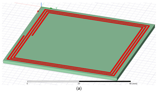
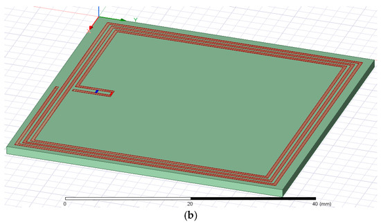
Figure 1.
The structures modeled and analyzed in Ansys: (a) the structure from Q3D Extractor; (b) the structure constructed in HFSS.
The dielectric used was FR4 Epoxy with dimensions of 47 × 47 × 1.51 mm. Following the analysis with Ansys Q3D Extractor (HEADQUARTERS Southpointe 2600 Ansys Drive Canonsburg, PA15317, USA), it was determined that the inductance value obtained through numerical modeling was close to the value calculated with Formula (1), as shown in Figure 2 [8,29,30].
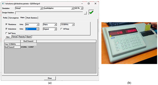
Figure 2.
The inductance values of the analyzed coil: (a) the values obtained from numerical modeling; (b) the values measured with the RLC meter.
After adapting the model to achieve resonance at 13.56 MHz, a capacitance value of 136 pF and a resistance of 50 Ω were used to be connected in parallel with the planar inductor. The capacitance value calculated analytically using Formula (2) was C = 132.464054 pF. Validation was also performed experimentally to determine the accuracy of the results. The structure was created using the LPFK S103 PCB production line, and its inductance was measured with an RLC Meter (Aim-TTi Glebe Road, Huntingdon, Cambridgeshire PE29 7DR, United Kingdom), as shown in Figure 2.
Figure 3 shows the testing setup, including the VNA and the measured S-parameters after a capacitor value of 130 pF and a resistance of 50 Ω were added to the terminals of the structure. It can be seen that results are in accordance with the results obtained analytically; thus, the formulas are verified.
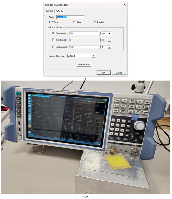
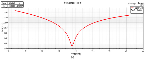
Figure 3.
The values of the circuit elements added to the circuit to achieve resonance at 13.56 MHz: (a) the values obtained from numerical modeling; (b) the resonance frequency measured after adding the circuit elements at the tag terminals; (c) the S parameters that confirm the operation of the structure at a resonance frequency very close to the desired value.
In Figure 3c, the resonant frequencies obtained after numerically modeling the structures with Ansys HFSS (HEADQUARTERS Southpointe 2600 Ansys Drive Canonsburg, PA 15317, USA) are shown.
The formulas for the inductance and capacitance are presented as follows:
where L is the inductance, is the permeability of the free space, N is the number of turns, and represents the average diameter of the inductor. The latter is calculated as the mean of the inner and outer diameters, calculated with Formula (3), where is the exterior diameter of the inductor, is the interior diameter of the inductor, is the fill factor, which is the ratio of the inner diameter to the outer diameter of the spiral inductor calculated with Formula (4), and are the coefficients that depend on the inductor’s shape. The value f in the formula used to calculate the capacitance C is the frequency value at which we want the inductor to resonate. In Formula (4), w represents the width of the turn, while s is the distance between the turns.
The values of the coefficients in Formula (1) depending on the shape of the inductor are found in Table 1.

Table 1.
The coefficients for the capacitance calculations based on the shape of the inductor.
The inductor shapes considered for this study can be observed in Figure 4.
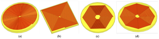
Figure 4.
Shapes considered for the planar inductor: (a) circular; (b) rectangular; (c) hexagonal; (d) octagonal.
3. Software Program Used for Determining Possible Structures
Given the standard dimensions of coils used as tags in RFID and considering their various shapes, as found in the specialized literature, calculation software was designed to generate all possible geometric configurations to model such coils [29]. The logical scheme on which this software is based can be observed in Figure 5.
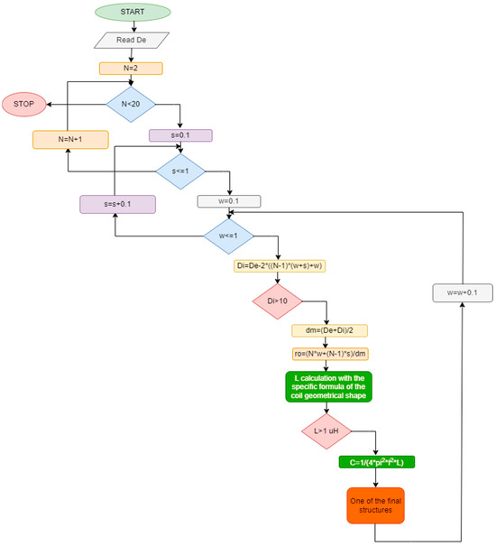
Figure 5.
The logical scheme underlying the program that determines the parameters of structures to meet the design conditions.
Thus, the exterior diameter () of the tag was considered to be a maximum of 20 mm for this study because of the usual dimension of such a tag, but the user can choose any other outer dimension. The parameters present in the logical scheme are as follows: N represents the number of turns of the coil, Di is the interior diameter of the coil, s is the distance between the coils, w is the width of the coil, dm is the medium diameter of the coil, and ro is the coil fill factor.
The inductance of the coils (L) has to exceed 1 µH, and the inner diameter () has to be at least 1 cm to later accommodate the necessary capacitor and resistor to achieve a resonance frequency of 13.56 MHz.
In this case, circular, square, hexagonal, and octagonal planar coils were considered. The formulas for calculating the inductance are given as (1), where the coefficients must be considered in accordance with the inductor’s shape.
The number of turns was limited to 20 in this study, but this can be reconfigured. The values of w and s were between 0.1 mm and 1 mm, considering a step of 0.1 mm.
For the imposed conditions, the most possible structures were obtained for the square configurations, as can be seen in Figure 6, for structures operating at 13.56 MHz.
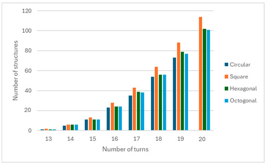
Figure 6.
The number of structures of different shapes that meet the design criteria for various values of the outer diameter.
Based on this algorithm, an interface was created using MATLAB R2023b (Corporate Headquarters: Natick, Apple Hill Campus 1 Apple Hill Drive Natick, MA 01760-2098 UNITED STATES). A window will open for the user, allowing them to select the desired structure type, as can be seen in Figure 7a. Next, they can enter the outer diameter for the structure in the interface that opens, as presented in Figure 7b.
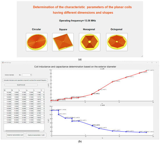
Figure 7.
The MATLAB interface for determining structures of interest: (a) the interface of the algorithm for determining the characteristic parameters for coil structures; (b) determination of the structures that meet the criteria in tabular and graphical form.
Upon pressing the “Calculate inductance and capacitance required to achieve the resonant frequency” button, all relevant variables that meet the requirements outlined in the logical scheme in Figure 5 will be calculated and displayed in a table.
The table will contain the exterior diameter, the number of turns, the distance between turns, the thickness of the winding, the inductivity of the spiral coil, and the capacitance value needed for the coil to reach the resonance frequency.
To work more easily with the values, the user can press the “Export to Excel” button, and an Excel file with the relevant data will be automatically generated. The inductance as a function of the number of turns is represented when pressing the “Graphical Representation L [uH]” button.
The information about the capacitance needed for the coil to resonate at 13.56 MHz is obtained in the second graph, which represents the capacitance of the structures as a function of the number of turns when the “Graphical Representation C [pF]” button is pressed.
Following the analysis with this software for circular coils with a maximum exterior diameter of De = 20 mm, 1883 possibilities were obtained, of which 299 met all the imposed conditions. Among these, the structures with the smallest outer diameters—namely 13 mm, 14 mm, and 15 mm—were modeled. These structures were modeled using Ansys Q3D Extractor and Ansys HFSS(HEADQUARTERS Southpointe 2600 Ansys Drive Canonsburg, PA 15317, USA), resulting in values very close to those obtained analytically, as shown in the graphs in Figure 8. The errors between the calculated values and those obtained through numerical modeling were between 4% and 6%, while for the capacitance values, the errors were between 4% and 10% due to the fact that the ports of the structures had different dimensions, which influences their values. Therefore, optimizing the length of the ports is necessary.
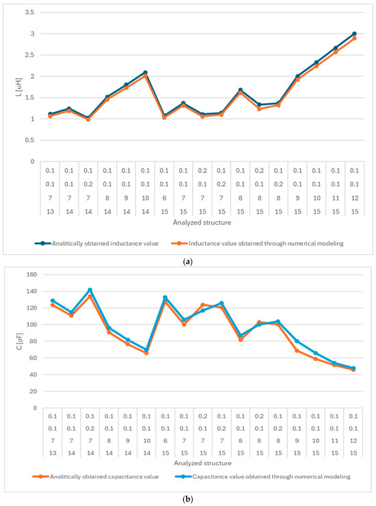
Figure 8.
Comparison between the analytical results and the results obtained through numerical modeling for (a) inductance and (b) capacitance.
The same process was carried out for the square structures, where, after applying the filters, 358 viable structures were obtained out of a total of 1883. For the hexagonal structures, 318 structures that met the constraints were obtained, and for the octagonal structures, there were 314 possible structures. Concordance between the analytically and numerically obtained values for all analyzed shapes can be observed in Figure 9, Figure 10 and Figure 11. It can be seen that for the capacitances, the errors increased, but it was observed that the positions and dimensions of the connecting wires between the capacitor and the coil somewhat influenced the capacitance values, so these differences are justified.
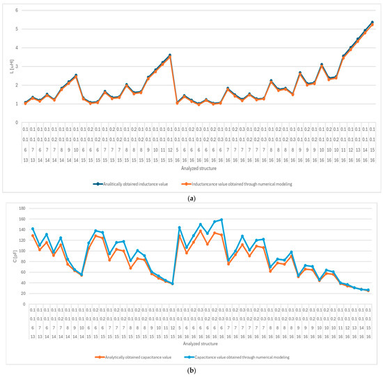
Figure 9.
Comparison between the numerically and analytically obtained values for the inductance and capacitance required to achieve resonance at 13.56 MHz for the square coil structures: (a) inductance; (b) capacitance.
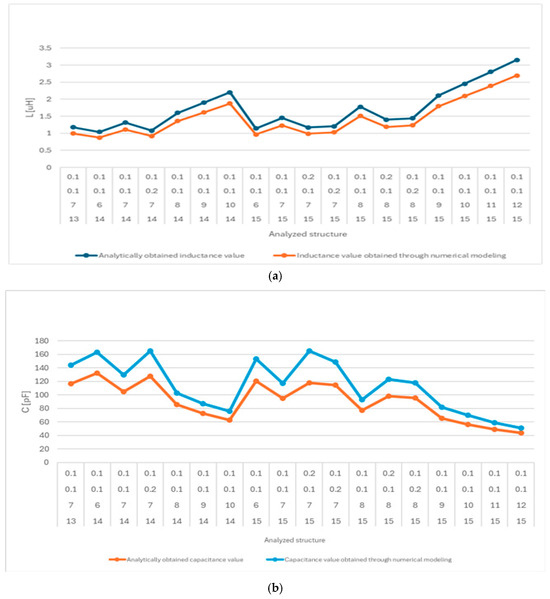
Figure 10.
Comparison between the numerically and analytically obtained values for the inductance and capacitance required to achieve resonance at 13.56 MHz for the hexagonal coil structures: (a) inductance; (b) capacitance.
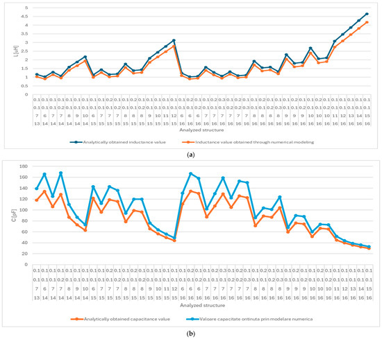
Figure 11.
Comparison between the numerically and analytically obtained values for the inductance and capacitance required to achieve resonance at 13.56 MHz for the octagonal coil structures: (a) inductance; (b) capacitance.
For the square planar structures, the errors between the calculated values and those obtained for the inductance through numerical modeling were between 2% and 5%, while the errors for the capacitance values were between 1% and 10%. For the hexagonal and octagonal planar inductors, the errors were a little bit higher due to their complexity. The values of the errors can be seen in Table 2 for a better comparison.
Table 2.
The errors between the results obtained analytically and through numerical modeling.
3.1. Influence of the Shape of the Inductor on the Gain Distribution
The second step of the study was analyzing the structures obtained from the gain point of view. To achieve this, the structures with an exterior diameter of 13 mm, seven turns, and a distance between the turns equal to the thickness of the turns with a dimension of 0.1 mm were compared. First, a 3D representation of the gain was considered, as shown in Figure 12, and it was determined that the shape of the coil did not significantly influence the shape of the gain, but the values were higher for the square coil.
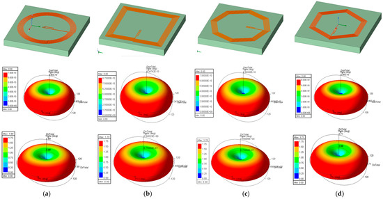
Figure 12.
Gain representation of four coil shapes: (a) circular; (b) square; (c) hexagonal; (d) octagonal.
In Table 3, the peak values of the gain and directivity of the considered structures are presented. It can be concluded that the square coil inductor radiated more than the others.
Table 3.
Peak values of the gain and directivity of the considered structures.
3.2. Influence of the Number of Turns on the Gain Distribution
Considering the fact that the number of turns can vary up to 20, the influence of the number of turns when considering the same exterior diameter is also an important matter.
In this study, two circular spiral structures with exterior diameters of 15 mm, w and s values of 0.1 mm, and 7 (Figure 13a) and 12 (Figure 13b) turns, respectively, were considered.
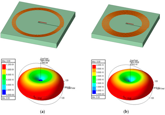
Figure 13.
Gain representation of two coil shapes with different numbers of turns: (a) N = 7; (b) N = 12.
The conclusion is that when the number of turns was higher, the gain was more evenly distributed on the surface of the tag, but the peak value of the higher number of turns was lower.
In Figure 14, Figure 15 and Figure 16, the gain and directivity of the obtained structures are presented for the structures with square and octagonal spiral coils and exterior diameters, of 13 mm, 14 mm, and 15 mm.
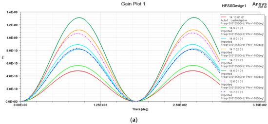
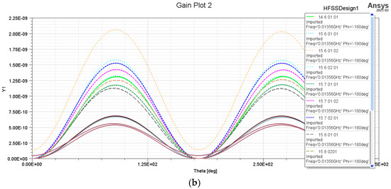
Figure 14.
Gain representation of exterior diameters of 13 mm, 14 mm, and 15 mm of the square spiral-shaped structures: (a) gain of the square-shaped coil structures with De = 13 mm and 14 mm; (b) gain of the square-shaped coil structures with De = 15 mm.
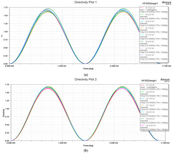
Figure 15.
Directivity representation of exterior diameters of 13 mm and 14 mm of the square and octagonal spiral-shaped structures: (a) directivity of the square-shaped coil structures; (b) directivity of the octagonal-shaped coil structures.
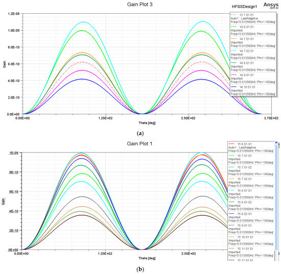
Figure 16.
Gain representation of exterior diameters of 13 mm, 14 mm, and 15 mm of the octagonal spiral-shaped structures: (a) gain of the octagonal-shaped coil structures with De = 13 mm and 14 mm; (b) gain of the octagonal-shaped coil structures with De = 15 mm.
It can be determined that the aforementioned conclusion is verified. Namely, when the number of turns increased, the maximum gain decreased for all the coil shapes considered in this study. Also, with the increases in the exterior diameter, the value of the gain also increased. There were two points at which the maximum gain was reached; therefore, the positioning of the tag is very important.
Considering all the coil shapes analyzed, the maximum gain values were obtained for the square coil planar structures.
The directivity was not considerably influenced by the number of turns or the exterior diameter, as can be seen in Figure 15a,b.
3.3. Influence of the Dielectric Material and Thickness on the Gain Distribution and Resonance Frequency
Dielectrics play an important role in the structures functioning at higher frequencies. Therefore, a study regarding their influence on the tag operation is crucial. Four different dielectrics were considered, as can be seen in Table 4, with different relative permittivity values varying from 2.2 to 10.2. For this study, we considered three different types of dielectrics from Rogers Corporation with different relative permittivity values and FR4 epoxy due to its wide range of use and the fact that it has a low cost. We considered the Rogers dielectrics due to their availability in our laboratory.
Table 4.
Dielectrics used for the study.
It can be stated that at low frequencies, the dielectrics do not considerably influence the gain of the structures, as can be observed in Figure 17; therefore, a dielectric with a lower price, like FR4 epoxy, was sufficient to achieve our goal.
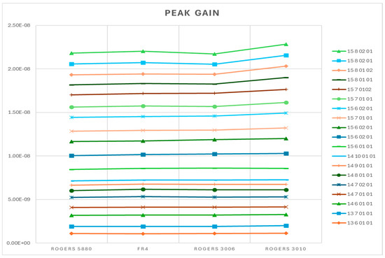
Figure 17.
Peak gain for square spiral coil structures with exterior diameters of 13 mm, 14 mm, and 15 mm.
As in previous representations, in the graph in Figure 14, the structures are named using their exterior diameters, number of turns, distance between the turns, and thickness of the turn. For example, for a structure with De = 14 mm, N = 7 turns, s = 0.1 mm, and w = 0.1 mm, the name is 14 7 01 01.
When considering the dielectric thickness, it was discovered that it influences the maximum gain of the structures but not in a linear manner; therefore, it is very hard to predict their operation. The influence of three different dielectric thicknesses, namely 0.51 mm, 1.27 mm, and 1.52 mm, is presented in Figure 18.
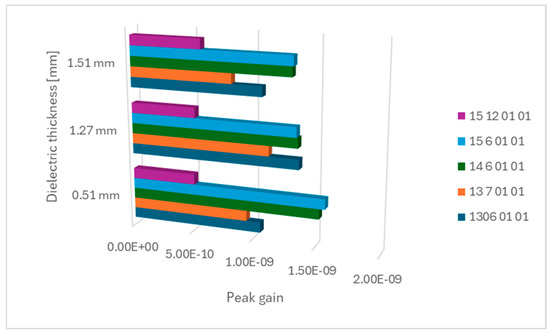
Figure 18.
The influence of the dielectric thickness on the peak gain of square coil structures.
Figure 19 presents the influence of changing the dielectric thickness of a structure with a dielectric thickness of 1.52 mm for which the circuit elements were considered for it to resonate at 13.56 MHz. It can be observed that the decreases in the dielectric thickness to 1.27 mm and 0.51 mm led to shifts in the resonant frequency.
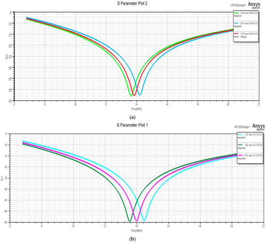
Figure 19.
The influence of the dielectric thickness on the resonance frequency.
4. Thermic Study of the Tag Structures Analyzed
For the thermal analysis of the structures, several configurations were considered for evaluation. In this case, a new module from the Ansys suite, namely Icepack, was used. Figure 20 presents only a few of the analyzed structures, specifically three structures with the smallest analyzed diameter of 13 mm, featuring 7 turns 0.1 mm thick, followed by three structures with an outer diameter of 15 mm, each with 12 turns 0.1 mm thick. It can be observed that, in ambient conditions, the temperature on the tag’s surface, as well as within the dielectric, did not exceed 40 °C, indicating that this temperature did not thermally or mechanically affect the analyzed tags in the short term.
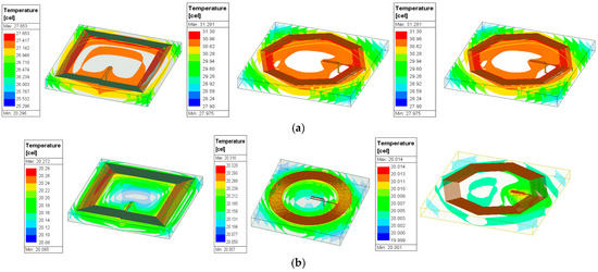
Figure 20.
The determined temperatures for the analyzed structures: (a) structures with an exterior diameter of 13 mm and 7 turns; (b) structures with an exterior diameter of 13 mm and 7 turns.
5. Discussions
Some of the structures presented above were created with the equipment from the laboratory, but due to their small dimensions, there were some limitations. This is why we considered creating some of the structures with s and w geometrical dimensions larger than 0.2 mm. The considered structures were the square planar coil ones due to the fact that they outperformed the other structures. Their inductance was calculated with the formulas, determined through numerical modeling and measured with an RLC meter. It can be seen that the values were in accordance (Table 5). The higher difference between the values obtained by the measurements was due to the presence of wires with a greater length at the terminals of the circuit. The values obtained for the capacitance necessary for the circuit to resonate at 13.56 MHz had higher values when obtained through numerical modeling, also due to the dimensions of the terminals of the circuit modeled in the Ansys program, but, as we know, the capacitors had specific values. Therefore, an approximation of this value was possible by analytical calculation or numerical modeling.
Table 5.
The characteristics of the structures along with the L and C values calculated, measured, and obtained through numerical modeling for the square-shaped spiral planar structures.
The structures were created with the help of LPKF Plotter (LPKF Laser & Electronics SE, LPKF Laser & Electronics SE, Osteriede 7. D-30827 Garbsen), and they are presented in Figure 21. The capacitance and inductance values obtained experimentally, analytically, and through numerical modeling are also compared in the graphs in Figure 22. The measuring process of the inductance can be seen in Figure 23 for each of the structures analyzed.
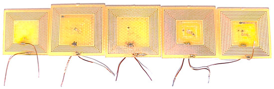
Figure 21.
The square structures constructed with the help of LPKF Plotter.
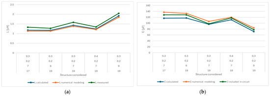
Figure 22.
A comparison of the obtained values through measurement, numerical modeling, and analytical calculations of (a) inductivity and (b) capacitance.
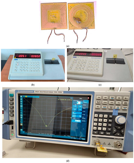
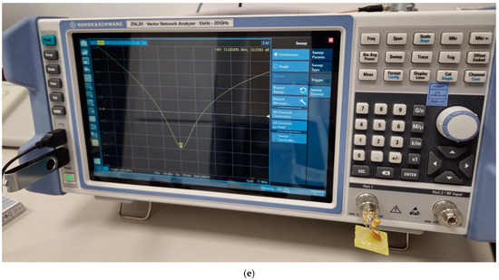
Figure 23.
The measurements of the characteristic parameters of the square and circular planar inductors: (a) structures to be measured; (b) inductance of the square planar inductor; (c) inductance of the circular planar inductor; (d) S parameters for the square planar inductor with circuit elements to resonate at 13.56 MHz; (e) S parameters for the circular planar inductor with circuit elements to resonate at 13.56 MHz.
In order to determine if the square structures were indeed better than the other shape planar structures, circular and square structures with an exterior diameter of 19 mm, nine turns, a spiral width of 0.3 mm, and a distance between the turns of 0.2 mm were constructed and compared. The structures are presented in Figure 23, along with the experimental measurements of the inductance values and the determination of the circuit elements placed on the planar structures in order for them to function at 13.56 MHz.
The results analytically obtained for the structures are in accordance with those obtained through numerical modeling and experimentally. Therefore, any of these methods could lead to optimal structure determination. For the structures to function at 13.56 MHz due to the specific values of the capacitors on the market, two capacitors were placed in parallel in order to reach the needed value. Namely, for the square-shaped structure, a capacitor of 68 pF was placed in parallel with a capacitor of 10 pF, while for the circular structure, the capacitors had values of 68 pF and 20 pF. For each structure, a resistance of 50 Ω was also placed in parallel with the capacitors.
As expected, for the same exterior diameter, the inductance of the square-shaped spiral inductor was higher. Therefore, a larger capacitor was needed for the structure to resonate at the needed frequency. In Table 6, the values are compared in order to determine their accuracy.
Table 6.
Values obtained for the circular and rectangular planar spiral inductors.
6. Conclusions
This study was conducted in order to improve RFID tags functioning at 13.56 MHz due to their versatility and wide range of applications in which they are used. Our main goal was to create an easily integrated structure with small dimensions and high gain, while also considering the decrease in manufacturing costs.
To achieve this, we first developed and implemented software designed to identify possible structures that meet specific conditions, such as the external diameter, an inductance greater than 1 µH, and an internal diameter large enough to accommodate circuit elements for operation at the target frequency of 13.56 MHz. The software enables users to quickly view all potential dimensions and make an informed selection. The accuracy of the results was validated through numerical modeling using Ansys Q3D Extractor and Ansys HFSS.
After evaluating four different shapes of planar inductors—square, circular, hexagonal, and octagonal—it was found that the algorithm used to create and implement the designs allows for additional possible structures under the given constraints. Furthermore, when comparing structures with the same number of turns and identical spacing (s) and width (w), square planar inductors were found to be superior due to their higher gain values. Analysis of the dielectric material revealed that the type of dielectric did not affect the structures’ output parameters, but changes in the dielectric thickness did influence the peak gain and resonance frequency. From a thermal perspective, temperature did not have a significant short-term thermal or mechanical impact on the tags studied.
As a general conclusion, the tags can be improved by decreasing their dimensions and using a cheap dielectric, although a larger exterior diameter is better, and a smaller number of turns provides better gain.
Author Contributions
Conceptualization, C.C., C.P., A.G. and C.M.; methodology, C.C., A.G. and C.P.; validation, C.C., A.G., C.P., M.G. and S.A.; formal analysis, C.C.; investigation, C.C., C.P., A.G. and C.M.; resources, S.A., R.L. and M.G.; data curation, C.C., C.P., A.G. and C.M.; writing—original draft preparation, C.C.; writing—review and editing, C.C., A.G. and C.P.; visualization, R.L., S.A. and M.G.; supervision, C.M.; project administration, C.C.; funding acquisition, C.C. All authors have read and agreed to the published version of the manuscript.
Funding
This research was funded by the Academy of Romanian Scientists, grant number 31/08.04.2024, “Digitalizarea procesului de proiectare al antenelor multifrecventa RFID si evaluarea expunerii umane la radiatiile emise de acestea”.
Institutional Review Board Statement
Not applicable.
Informed Consent Statement
Not applicable.
Data Availability Statement
The data are contained within the article.
Acknowledgments
This work was supported by a grant from the Academy of Romanian Scientists, project title: Digitalization of the Design Process for Multifrequency RFID Antennas and Evaluation of Human Exposure to the Radiation Emitted by Them.
Conflicts of Interest
The authors declare no conflicts of interest.
References
- Jiang, C.Y.; Wong, C.I.; Chio, C.H.; Tam, K.W.; Choi, W.W.; Teng, C. A Wireless Motion Capture System for Shoulder Rehabilitation based on RFID Passive Tag Antenna Array. In Proceedings of the 2021 IEEE International Conference on RFID Technology and Applications (RFID-TA), Delhi, India, 6–8 October 2021; pp. 16–19. [Google Scholar] [CrossRef]
- Turki, B.; Ziai, M.A.; Hillier, A.; Belsey, K.; Parry, A.; Yeates, S. Chemical Vapor Detecting Passive RFID Tag. In Proceedings of the 2019 IEEE International Conference on RFID Technology and Applications (RFID-TA), Pisa, Italy, 25–27 September 2019; pp. 113–115. [Google Scholar] [CrossRef]
- Haider, U.A.; Noman, M.; Rashid, A.; Rmili, H.; Ullah, H.; Tahir, F.A. A Semi-Octagonal 40-Bit High Capacity Chipless RFID Tag for Future Product Identification. Electronics 2023, 12, 349. [Google Scholar] [CrossRef]
- Luo, J.; Xue, R.; Cheong, J.; Zhang, X.; Yao, L. Design and Optimization of Planar Spiral Coils for Powering Implantable Neural Recording Microsystem. Micromachines 2023, 14, 1221. [Google Scholar] [CrossRef] [PubMed]
- Yang, X.; Ding, Z.; Zhang, Z. A Complete Flow of Miniaturizing Coil Antennas Based on Matching Circuit. Electronics 2021, 10, 1159. [Google Scholar] [CrossRef]
- Victoria, J.; Suarez, A.; Martinez, P.A.; Alcarria, A.; Gerfer, A.; Torres, J. Improving the Efficiency of NFC Systems Through Optimizing the Sintered Ferrite Sheet Thickness Selection. IEEE Trans. Electromagn. Compat. 2020, 62, 1504–1514. [Google Scholar] [CrossRef]
- Dakić, B.; Damnjanović, M.; Živanov, L.; Menićanin, A.; Blaž, N.; Kisić, M. Design of RFID antenna in ink-jet printing technology. In Proceedings of the 2012 IEEE 10th Jubilee International Symposium on Intelligent Systems and Informatics, Subotica, Serbia, 20–22 September 2012; pp. 429–432. [Google Scholar] [CrossRef]
- Pacurar, C.; Topa, V.; Giurgiuman, A.; Munteanu, C.; Constantinescu, C.; Gliga, M.; Andreica, S. Planar Spiral Inductors Parameter Extraction needed to design a Wireless Power Supply System. In Proceedings of the 2021 9th International Conference on Modern Power Systems (MPS), Cluj-Napoca, Romania, 16–17 June 2021; ISBN 978-1-6654-3381-5. WOS:000941563300104. [Google Scholar] [CrossRef]
- Mazumder, K.; Ghosh, A.; Bhattacharya, A.; Ahmad, S.; Ghaffar, A.; Hussein, M. Frequency Switchable Global RFID Tag Antennae with Metal Compatibility for Worldwide Vehicle Transportation. Sensors 2023, 23, 3854. [Google Scholar] [CrossRef]
- Ojaroudi Parchin, N.; Jahanbakhsh Basherlou, H.; Abd-Alhameed, R.A.; Noras, J.M. Dual-Band Monopole Antenna for RFID Applications. Future Internet 2019, 11, 31. [Google Scholar] [CrossRef]
- Corchia, L.; Monti, G.; Tarricone, L. A Frequency Signature RFID Chipless Tag for Wearable Applications. Sensors 2019, 19, 494. [Google Scholar] [CrossRef]
- Cavaliere, M.; Jaeger, H.A.; O’Donoghue, K.; Cantillon-Murphy, P. Planar Body-Mounted Sensors for Electromagnetic Tracking. Sensors 2021, 21, 2822. [Google Scholar] [CrossRef]
- Ma, Z.; Jiang, Y. High-Density 3D Printable Chipless RFID Tag with Structure of Passive Slot Rings. Sensors 2019, 19, 2535. [Google Scholar] [CrossRef]
- Khan, S.R.; Choi, G. Analysis and Optimization of Four-Coil Planar Magnetically Coupled Printed Spiral Resonators. Sensors 2016, 16, 1219. [Google Scholar] [CrossRef]
- Kim, E.S.; Kim, N.Y. Micro-Fabricated Resonator Based on Inscribing a Meandered-Line Coupling Capacitor in an Air-Bridged Circular Spiral Inductor. Micromachines 2018, 9, 294. [Google Scholar] [CrossRef] [PubMed]
- Shin, Y.; Woo, S. Reactive Shield for Reducing the Magnetic Field of a Wireless Power Transfer System with Dipole Coil Structure. Electronics 2024, 13, 1712. [Google Scholar] [CrossRef]
- Sugumar, S.; Santhanam, S.M. PCB Planar and Filamentary Planar Spiral Coils based Underground Magnetic Induction Communication with Enhanced Channel Model. Wirel. Pers Commun. 2021, 120, 1145–1170. [Google Scholar] [CrossRef]
- Sonntag, C.; Lomonova, E.A.; Duarte, J. Implementation of the Neumann formula for calculating the mutual inductance between planar PCB inductors. In Proceedings of the 18th International Conference on Electrical Machines, 2008, ICEM 2008, Vilamoura, Portugal, 6–9 September 2008. [Google Scholar] [CrossRef]
- Pacurar, C.; Topa, V.; Giurgiuman, A.; Munteanu, C.; Constantinescu, C.; Gliga, M.; Andreica, S. High Frequency Analysis and Optimization of Planar Spiral Inductors Used in Microelectronic Circuits. Electronics 2021, 10, 2897. [Google Scholar] [CrossRef]
- Demori, M.; Baù, M.; Dalola, S.; Ferrari, M.; Ferrari, V. Low-Frequency RFID Signal and Power Transfer Circuitry for Capacitive and Resistive Mixed Sensor Array. Electronics 2019, 8, 675. [Google Scholar] [CrossRef]
- Hussain, I.; Woo, D.-K. Inductance Calculation of Single-Layer Planar Spiral Coil. Electronics 2022, 11, 750. [Google Scholar] [CrossRef]
- Lin, C.; Zhan, T.; Wang, J.; Li, J.; Liu, Z.; Yi, X. Investigations about Al and Cu-Based Planar Spiral Inductors on Sapphire for GaN-Based RF Applications. Appl. Sci. 2021, 11, 5164. [Google Scholar] [CrossRef]
- Aldoumani, M.; Yuce, B.; Zhu, D. Using the Variable Geometry in a Planar Inductor for an Optimised Performance. Electronics 2021, 10, 721. [Google Scholar] [CrossRef]
- Chen, H.-H.; Hsu, Y.-W. Analytic Design of on-Chip Spiral Inductor with Variable Line Width. Electronics 2022, 11, 2029. [Google Scholar] [CrossRef]
- Liu, Q.; Zhang, Z. An Enhanced Six-Turn Multilayer Planar Inductor Interleaved Winding Design for LLC Resonant Converters with Low Current Ringing. Electronics 2024, 13, 3201. [Google Scholar] [CrossRef]
- Roh, S.; Nguyen, T.D.; Lee, J.S. Applications of Nanomaterials in RFID Wireless Sensor Components. Appl. Sci. 2024, 14, 1216. [Google Scholar] [CrossRef]
- Nizioł, M.; Jankowski-Mihułowicz, P.; Węglarski, M. Determination of Parameters of Radio Frequency Identification Transponder Antennas Dedicated to IoTT Systems Located on Non-Planar Objects. Electronics 2024, 13, 2800. [Google Scholar] [CrossRef]
- Kumar, S.; Buckley, J.; Barton, J.; O’Flynn, B. Performance analysis of a novel flexible NFC Tag for IoT applications. In Proceedings of the Smart System Integration 2018-12th International Conference and Exhibition on Integration Issues of Minituarized Systems, Dresden, Germany, 11–12 April 2018; pp. 432–435. [Google Scholar]
- Păcurar, C.; Topa, V.; Munteanu, C.; Racasan, A.; Hebedean, C. Studies of Inductance Variation for Square Spiral Inductors using CIBSOC Software. Environ. Eng. Manag. J. 2013, 12, 1161–1169. [Google Scholar] [CrossRef]
- Zhao, P.; Wang, J.; Xia, H.; He, W. A novel industrial magnetically enhanced hydrogen production electrolyzer and effect of magnetic field configuration. Appl. Energy 2024, 367, 123402. [Google Scholar] [CrossRef]


Disclaimer/Publisher’s Note: The statements, opinions and data contained in all publications are solely those of the individual author(s) and contributor(s) and not of MDPI and/or the editor(s). MDPI and/or the editor(s) disclaim responsibility for any injury to people or property resulting from any ideas, methods, instructions or products referred to in the content. |
© 2024 by the authors. Licensee MDPI, Basel, Switzerland. This article is an open access article distributed under the terms and conditions of the Creative Commons Attribution (CC BY) license (https://creativecommons.org/licenses/by/4.0/).