Article

A Fully Integrated High Linearity CMOS Dual-Band Power Amplifier for WLAN Applications in 55-Nm CMOS

1
Institute of Microelectronics of the Chinese Academy of Sciences, Beijing 100029, China
2
School of Electronic, Electrical and Communication Engineering, University of Chinese Academy of Sciences, Beijing 100049, China
3
Zhejiang CASEMIC Electronics Technology Co., Ltd., Hangzhou 310051, China
*
Authors to whom correspondence should be addressed.
Appl. Sci. 2024, 14(23), 10768; https://doi.org/10.3390/app142310768
Submission received: 15 October 2024 / Revised: 6 November 2024 / Accepted: 8 November 2024 / Published: 21 November 2024
(This article belongs to the Special Issue Applications of Wireless and Mobile Communications)

Abstract

:
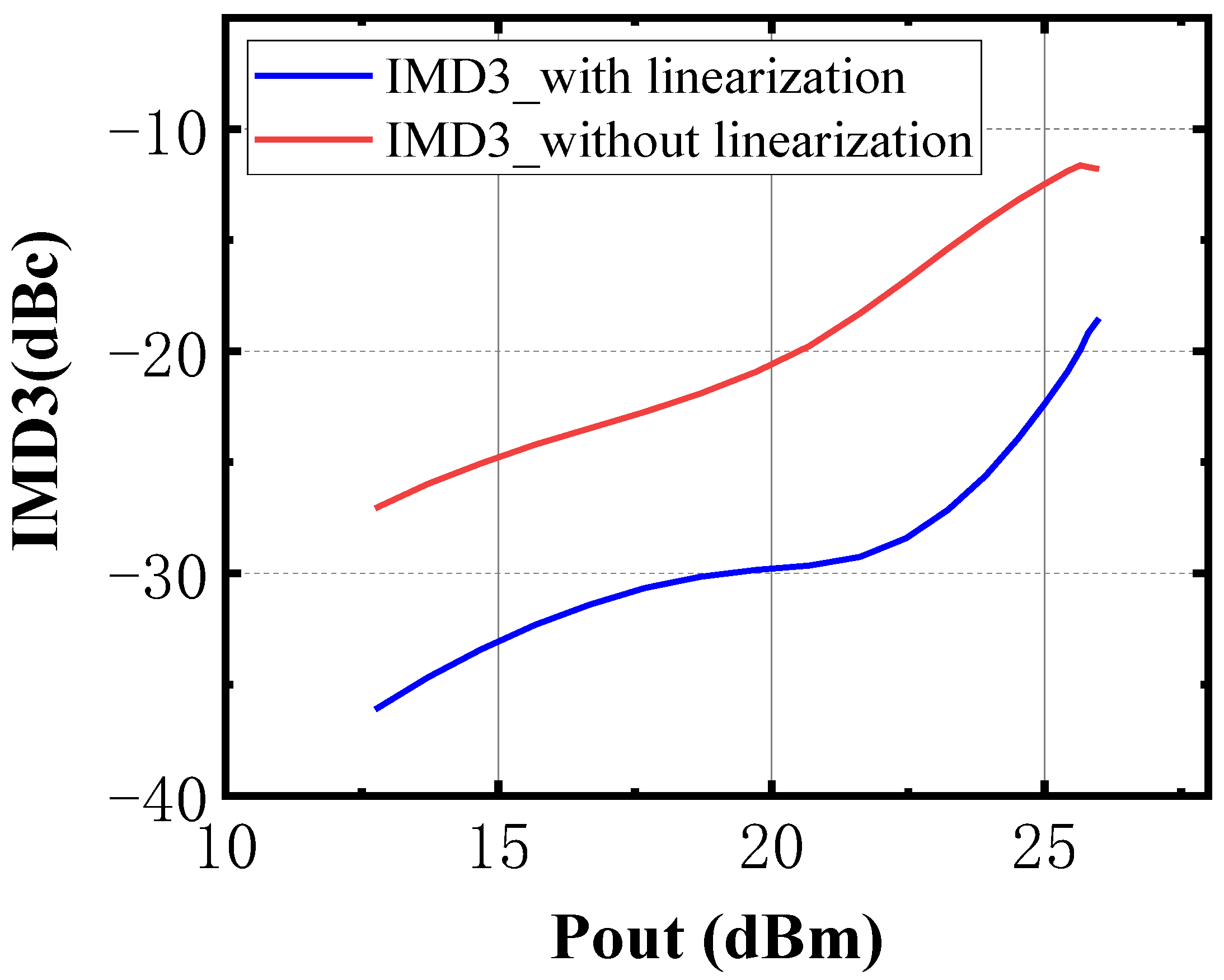
This paper presents a dual-band fully integrated high linearity CMOS power amplifier (PA). The PA employs a reconfigurable transformer in the input matching network to achieve low reflection coefficient across both bands, demonstrating significant flexibility in the design of dual-band power amplifiers with high output powers. Additionally, a detailed design methodology for the dual-band matching network is introduced. By utilizing this methodology, the PA has been designed using 55 nm CMOS technology. For continuous-wave operation, the PA achieves a saturated power ( P s a t ) of 28.03 dBm and 27.5–28.2 dBm, with power-added efficiency (PAE) of 33.2% and 24.6–31.1%, in the 2.4 GHz and 5 GHz WLAN bands, respectively. Concurrently, the PA power cells, which employ multi-gate transistor (MGTR) technology, achieve an intermodulation distortion (IMD3) of below 30 dBc at an output power of 15 dBm in both the 2.4 GHz and 5 GHz WLAN bands. The proposed PA outperforms other dual-band or multi-band PAs in terms of output power and exhibits great potential for WLAN applications.

1. Introduction

In recent years, wireless local area network (WLAN) technology has experienced rapid development and application across billions of mobile devices such as computers, smartphones, and tablets. To meet the requirements of high data throughput applications such as video conferences and 4K video streaming, WLAN standards have continuously increased signal bandwidth and adopted more advanced techniques. The current 802.11ax standard utilizes OFDMA technology and a 1024 QAM modulation scheme to boost data throughput, achieving a data rate of 9.6 Gbps. The development of new WLAN standards is drawing much effort in academia and industry. Additionally, system-on-chip (SoC) implementation with CMOS technology for WLAN applications has been the focus of attention in recent years [1,2,3,4,5,6].
IEEE 802.11ax devices need to operate in two frequency bands and also require compatibility with previous WLAN standards. Integrating multiple channel transceivers operating in different bands on a single chip is a common approach [7,8,9,10,11]. However, this approach results in a large chip area, which means the cost will be high. A preferable alternative is using a single transceiver supporting reconfigurable 2.4/5 GHz operation.
As the core block of the transmitter, power amplifiers should also support either dual-band or broadband operation, with a bandwidth that covers at least both the 2.4 GHz to 5 GHz bands. Currently, the design of broadband power amplifiers primarily relies on high-order matching networks [12,13,14,15,16]. However, for broadband amplifiers that comply with IEEE 802.11ax standards, the required operating bandwidth is extensive (at least from 2.4 GHz to 5.9 GHz), which necessitates a substantial matching network area. Furthermore, because high-order matching networks require multiple inductors or transformers for matching, they inherently increase matching network losses and significantly reduce the power amplifiers’ efficiency. Consequently, dual-band or multi-band power amplifiers employing switching capacitors or varactors [17,18,19,20] are more effectively suited for reconfigurable transmitters. However, the output power of current dual- or multi-band power amplifiers are not sufficiently high for certain WLAN applications (typically below 26 dBm). To address this issue, this paper aims to design a fully integrated dual-band power amplifier with improved output power. Additionally, existing dual- and multi-band power amplifier design methodologies struggle to meet high power output requirements. This paper proposes a new design methodology focused on optimizing the insertion loss of the matching network to achieve dual-band matching. This proposed methodology is highly universal and easily replicable. Based on the proposed design methodology, this paper develops a low-loss matching network, enabling the power amplifier to achieve sufficiently high output power. On the other hand, while some optimization methods for improving power amplifier linearity have been proposed [21,22,23], existing dual- or multi-band power amplifiers lack specific explanations and optimizations for linearity. This paper analyzes the causes of nonlinearity in power amplifiers and employs multi-gate transistor (MGTR) [24] technology to enhance linearity, enabling the power amplifier to achieve high linear output power.
The paper is organized as follows: Section 2 first introduces the topology of reconfigurable dual-band output matching network and then proposes a design methodology for the dual-band matching network based on passive insertion loss at both 2.4 GHz and 5 GHz. Finally, a reconfigurable transformer is thoroughly studied and subsequently employed in the proposed dual-band input matching network to achieve a low reflection coefficient across both bands. Section 3 describes the detailed circuit implementations. Section 4 presents the simulation results of the proposed CMOS PA. Section 5 discusses the research direction of CMOS PAs for WLAN applications, and Section 6 concludes this article.

2. Design of Dual-Band Matching Networks

2.1. Design of Dual Band Output Matching Networks

The design of the dual-band output matching network is crucial to achieving high output power across dual frequency bands. To achieve this goal, the dual-band output matching network should transform the 50 ohm impedance to the optimum load impedance of the power amplifier at both frequency bands. Additionally, the dual-band output matching network is required to maintain minimal loss at both frequency bands. This paper employs the reflection coefficient and insertion loss of the dual-band output matching network as guidance.
The optimal load impedance of the PA is given by a load resistance in parallel with an equivalent negative capacitance [17] and determined through load-pull simulations, as
Z o p t ω = R o p t / / 1 j ω C o u t
In this design, the simplified output matching schematic is shown in Figure 1. The reconfigurable output matching network comprises a fixed transformer and switching capacitors C s w s , which can adjust the load impedance seen in the matching network to achieve the optimum impedance in the two bands of interest. Ideally, the reflection coefficient Γ i n s = 0 and I L o u t p u t = 0 . However, due to the Bode-Fano limit [25] and transformer parasitic resistance, the ideal matching network is unachievable. Thus, in practice, we set | Γ i n s | 20   dB and | I L o u t p u t | 1.5   dB as the target.
The Z-parameter matrix for the transformer is as follows [26]:
Z = R p + j ω L p j ω M j ω M ( R s + j ω L s )
where
M = k L p L s
and k represents the coupling factor between primary and secondary coils.
Therefore, the equivalent load impedance for the power amplifier (PA) can be derived as Equation (4).
Z l o a d = R p + ω M 2 R s + R e q R s + R e q 2 + ω L s + X e q 2 + j ω L p ω M 2 ω L s + X e q R s + R e q 2 + ω L s + X e q 2
where
R e q = R L 1 + ω R L C s w s 2
X e q = ω R L 2 C s w s 1 + ω R L C s w s 2
So | Γ i n s | and IL can be derived as
Γ i n s = 20 l o g Z i n s R o p t Z i n s + R o p t
I L o u t p u t = 20 l o g j ω M R s + R e q + j ω L s + X e q · C o u t Z i n s Z i n s + R o p t C o u t · R o p t R L
where
Z i n s = C o u t / / Z l o a d
It can be seen that there are three main parameters ( L p ,   L s and C s w s ) to be determined. Considering the matching target, we calculate the minimum value of the | Γ i n s | and IL by sweeping values of the main parameters to find the optimum value range of L p and L s , where the value of C s w s is chosen to minimize the reflection coefficient and insertion loss. During this process, the quality factors of transformer windings are both assumed to be 12 at 2.45 G and 14 at 5.5 G, while the coupling factor of transformer windings is assumed to be 0.75, which are reasonable values for practical transformers in CMOS process. In addition, the value range of C s w s is limited to 0–3 pF, and the value of C s w s above 3 pF is regarded as unacceptable and is abandoned because of the low quality factor and large off-state capacitance ( C o f f ). So far, the values of the components in the proposed dual-band output matching network have been preliminarily determined.

2.2. Implementation of Dual-Band Output Matching Network

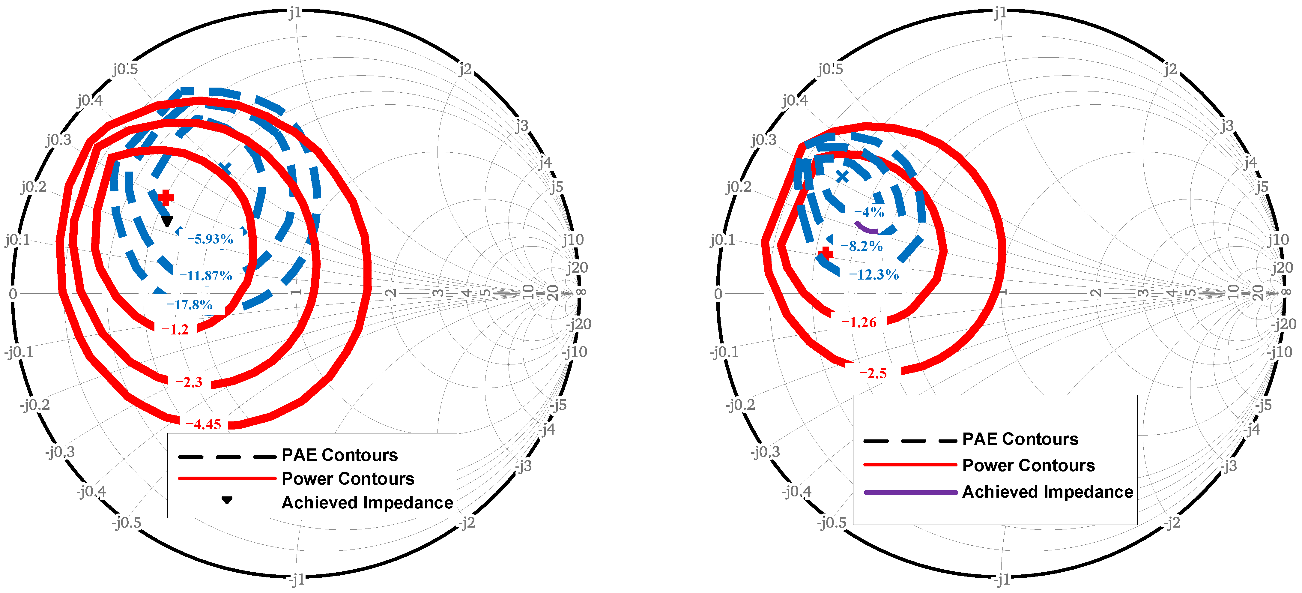
Now, we can take the next step to implement the dual-band output matching network according to the proposed methodology. The simulated power and PAE contours for 2.4 and 5.5 GHz are shown in Figure 2. In general, the pursuit is not singularly focused on either efficiency or output power; instead, a tradeoff between output power and PAE is normally made. In this design, the optimal load impedances are determined as 15.05 + j15.08 at 2.45 G and 9.87 + j15.86 and 5.5 G, respectively. The corresponding R o p t and C o u t are 30.17 Ω and 2.16 pF at 2.4 GHz and are 35.36 Ω and 1.32 pF at 5.5 GHz.
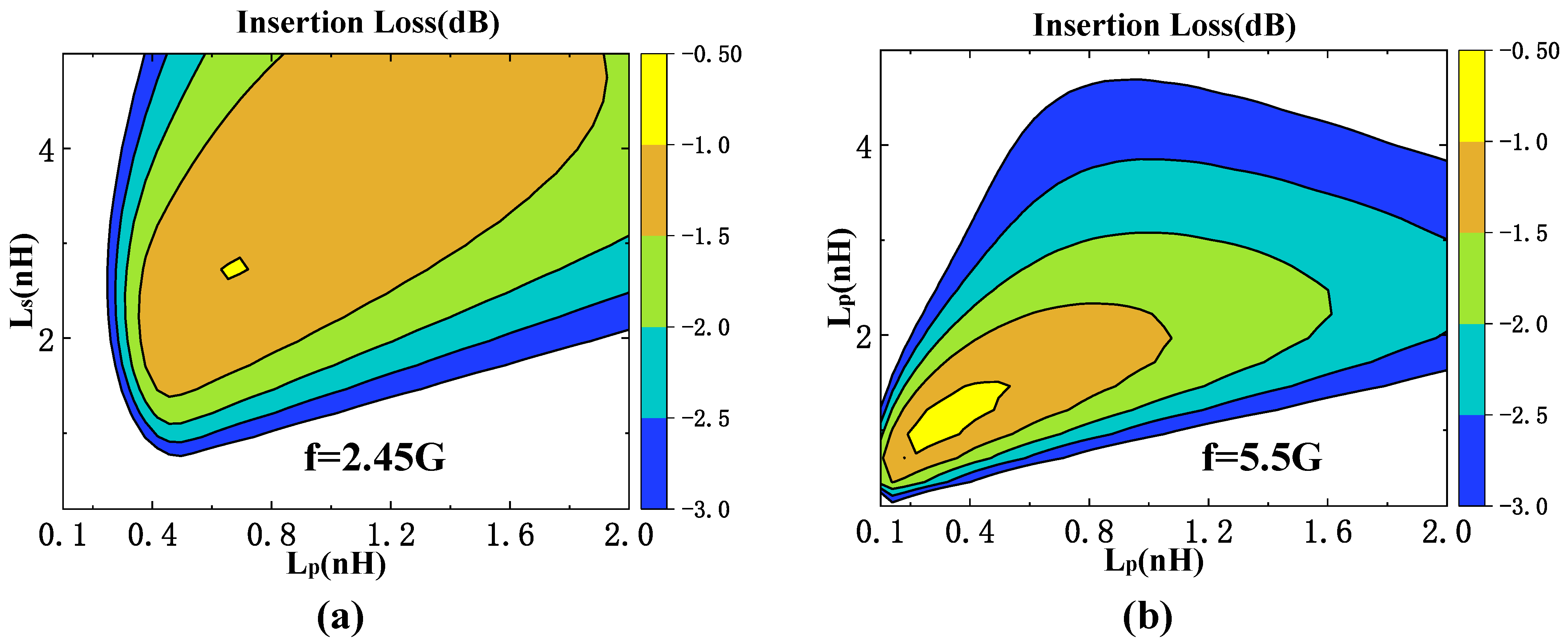
Therefore, the calculated values of the | Γ i n s | and IL are plotted in Figure 3 and Figure 4. Thus, we now have the optimum values of L p , L s , and C s w s .
We then take the next step to implement the output matching network with optimum values. In this design, the used CMOS process only has one thick metal layer. Consequently, all inductor coils are designed using the thickest metal layer with an octagonal shape to enhance the Q value of the inductors. To further improve the quality factor of the transformer, this design integrates a patterned ground shielding (PGS), constructed from poly layers, into the on-chip transformer to mitigate substrate losses. Simultaneously, a low doping substrate beneath the transformer is used to increase resistivity, thereby reducing the substrate magnetic losses. Therefore, the total layout of the transformer is depicted in Figure 5, and the parameters obtained from electromagnetic (EM) simulation for L p , L s , and k are as shown in Table 1.
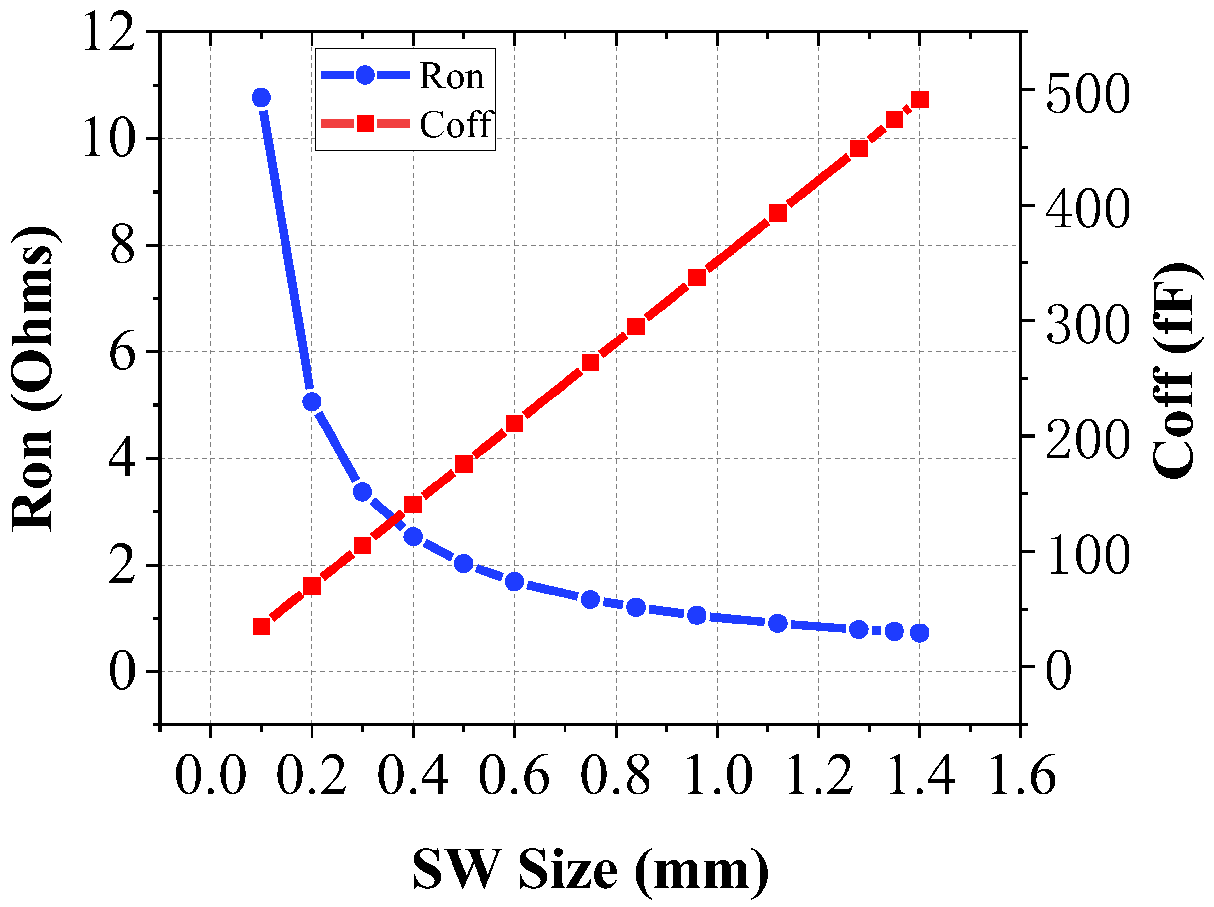
The schematic of the switching capacitor is shown in Figure 14. Two stacked thick-gate transistors are used, considering reliability when the switch is closed [16,27]. The quality factor of the switching capacitor is mainly determined by the on-resistance of the switching transistors, while the on-resistance is determined by the size of the transistor. To increase the quality factor of the switching capacitor, larger transistor sizes are preferred. However, larger transistor sizes result in a larger parasitic capacitance in the off state, which is a capacitance that must be considered in the matching network. Therefore, the size of the switch needs to be carefully balanced, taking into account both on-state resistance and off-state capacitance.
The on-resistance and off-state parasitic capacitance have been simulated for different transistor sizes, as shown in Figure 6. In this design, the C s w s is 1.37 pF, and the switching transistor size is 900 µm/280 nm. Furthermore, by using parallel switching capacitors, the parasitic resistance of the overall switching capacitors can be further reduced when the switches are closed.
Finally, the achieved output load impedance and the insertion loss of the output matching network in this design are shown in Figure 1 and Figure 7. The insertion loss is higher than the target at the 5.5 GHz band due to the requirement of operating bandwidth at 2.4 G bands. The value of the transformer windings ( L p ,   L s ) cannot be too small, causing larger insertion loss in 5.5 GHz band, and the degradation of the insertion loss is acceptable in practice. The simulation results demonstrate that the implemented output matching network exhibits superior matching performance across both the 2.4 GHz and 5 GHz frequency bands, fully validating the effectiveness of the dual-band matching network design methodology presented in this work.

2.3. Implementation of Dual-Band Input Matching Network

Different from the output matching, input matching is more sensitive to inductor and capacitor values. Small variations can have a significant impact on the reflection coefficient, making it challenging to achieve good matching within dual bands at high output power conditions. To address this issue, this article proposes a novel reconfigurable input matching circuit. The schematic is shown in Figure 8, and the input matching circuit consists of the switching capacitors and reconfigurable transformers. Applying a reconfigurable transformer significantly enhances dual-band input matching under high output power conditions. At the high-frequency band (5 GHz), the inductance values of the reconfigurable transformer decrease, ensuring effective input matching. Conversely, at the low-frequency band (2.4 GHz), the inductance values increase, facilitating optimal input matching at the lower band.
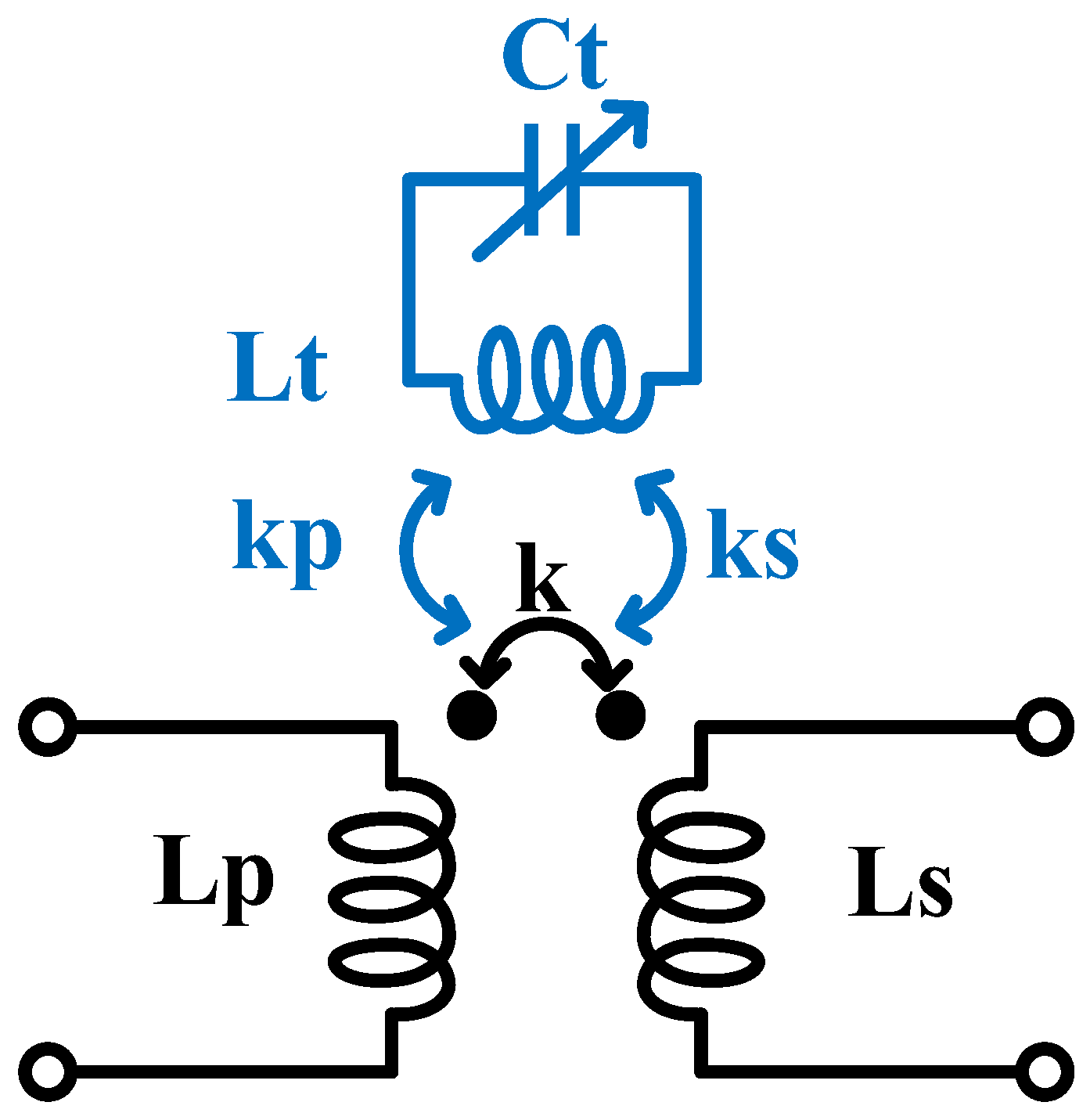
The simplified schematic of the reconfigurable transformers is shown in Figure 9:
The reconfigurable transformer is composed of the main transformer windings ( L p , L s ), tuning inductor L t , and tuning capacitor C t . The tuning inductor L t is magnetically coupled to the main transformer with coupling coefficients k p and k s , which is also connected directly with the tuning capacitor C t . The reconfigurable transformer is based on a tunable inductor, which is shown in Figure 10. The R t is the parasitic resistance of the entire tuning branch, which includes the parasitic resistances of both the resonant inductor L t and the switching capacitor C t . When the main inductor L 1 inputs a signal, the induced current I t through L t and C t will generate an induced magnetic field. Thus, the total magnetic flux of the main inductor is influenced by the induced magnetic field, and so the equivalent inductance of the main inductor will be changed and can be derived as Equation (8).
L e q = L 1 + L 1 L t C t k t 2 ω 2 1 L t C t ω 2 L t C t ω 2 1 2 + R t 2 C t 2 ω 2
R e q = R 1 + C t 2 L 1 L t R t k t 2 ω 4 L t C t ω 2 1 2 + R t 2 C t 2 ω 2
Q e q = 1 C t 2 L t 2 k t 2 1 ω 4 + C t R t 2 C t + L t k t 2 2 ω 2 ω L 1 C t 2 L t L 1 R t k t 2 + R 1 L t ω 4 + C t R 1 R t 2 C t 2 L t ω 2 + R 1
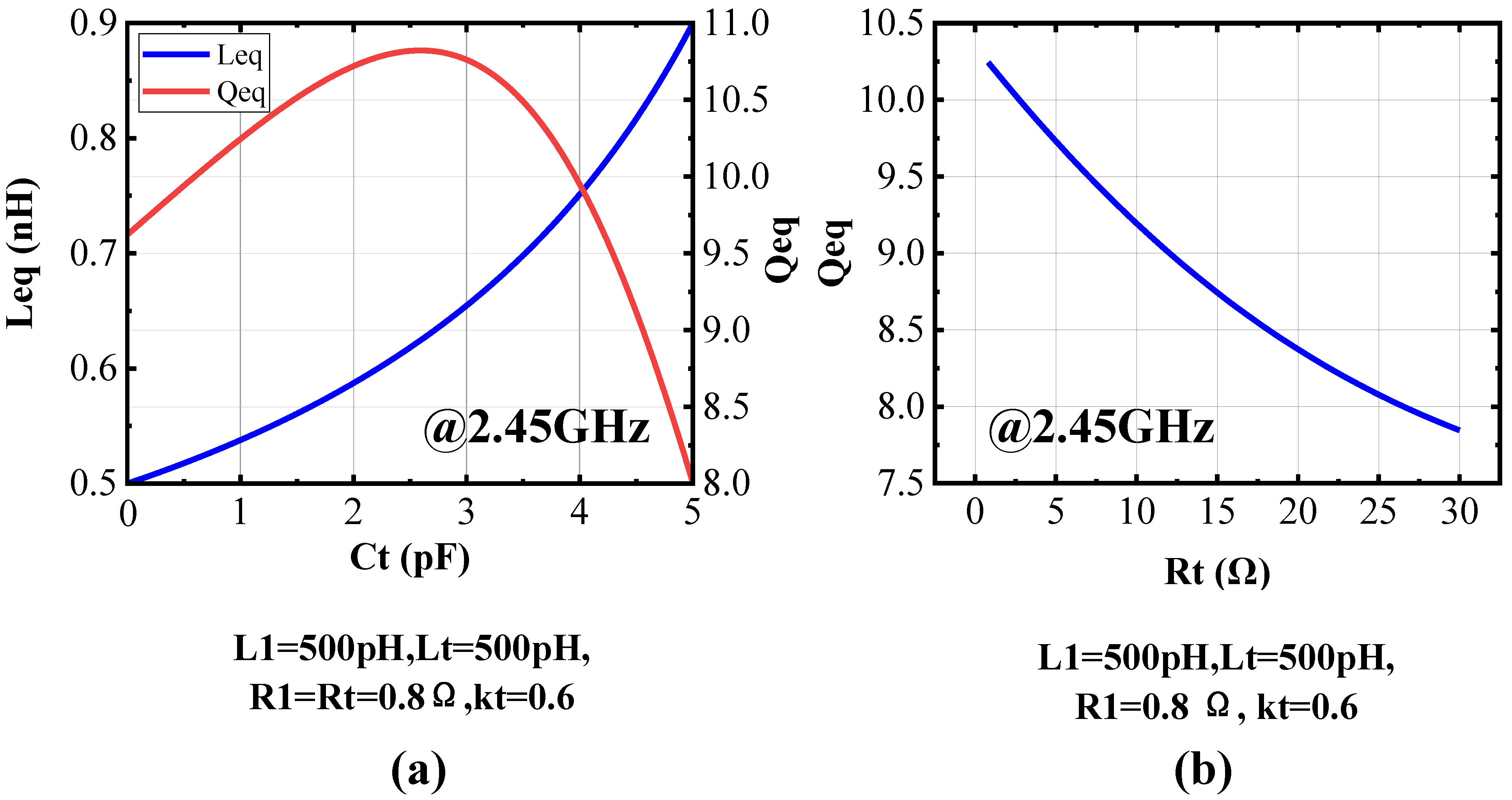
Meanwhile, due to magnetic coupling, the quality factor of the main inductor is also manipulated and is derived as Equation (10). Figure 11a illustrates the variations in main inductance value and Q factor when the tuning capacitor C t changes. Figure 7b shows the impact of R t on the main quality factor. It can be seen that the values of the main inductor ( L 1 ) and quality factor (Q) are significantly influenced by the tuning capacitor, while quality factor has low relativity to R t , indicating that the tuning capacitor should be within an appropriate range to prevent a severe reduction in Q. On the other hand, changing the tuning capacitor within the appropriate range allows for changes in inductance with minimal impact on the Q factor. The reconfigurable transformer in this work is formed by one tunable inductor L t . Thus, the values of the main reconfigurable transformer windings are influenced by L t , C t with coupling factor k p , k s .
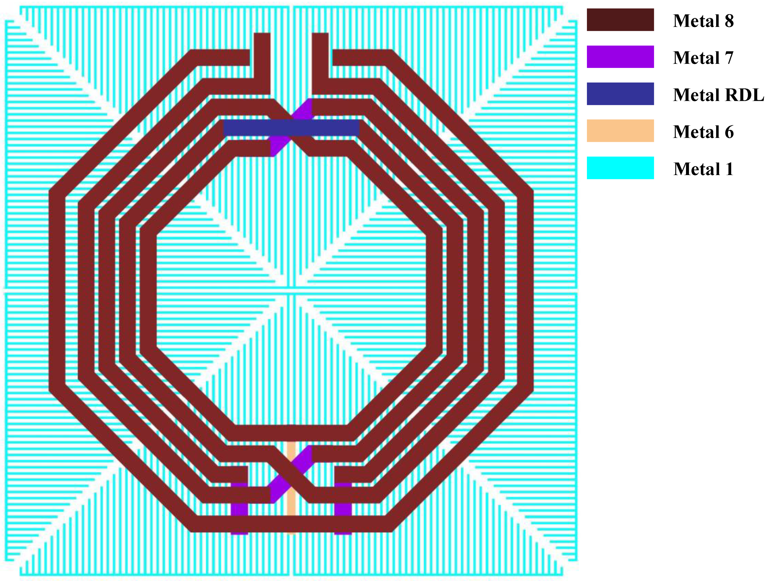
By applying the proposed dual-band matching network design methodology, the required transformer parameters of the input matching network can be determined. Moreover, the incorporation of the reconfigurable transformer in this work substantially expands the inductance range of the practical transformer, thereby enabling more effective dual-band input matching. We then take the next step to implement the input matching network with optimum values. The layout of the reconfigurable transformer is shown in Figure 12, with a turn ratio of 2:2 for the main transformer and the tuning coil located on the outermost layer. All inductor coils employ the same metal layer to enhance the quality factor of the transformer. To avoid a significant impact on the Q values of L p and L s , the maximum value of C t should not exceed 3 pF. The value of C t in this design is 2.8 pF.
When the switching capacitor C t changes, the values of the reconfigurable transformer are changed and are shown in the table below.
It can be seen that the proposed reconfigurable transformer in this paper achieves a change of approximately 100 pH in inductance with an acceptable decrease in Q. This feature is advantageous for achieving dual-band input matching. The final schematic of the dual-band input matching network is shown in Figure 8. The transistor sizes of the switch C i n p and C t are 450 µm/280 n and 540 µm/280 n, respectively. The off capacitances of the switches are 307 fF and 513 fF. The parameter of the reconfigurable transformer is shown in Table 2.
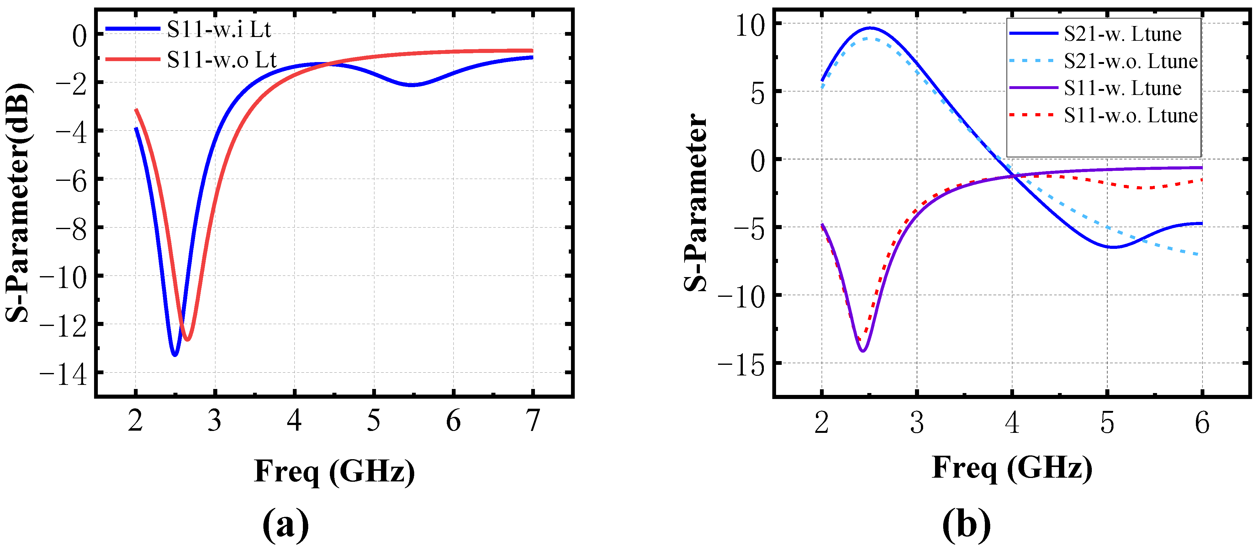
In comparison to a fixed transformer, the reconfigurable transformer proposed in this article demonstrates excellent impedance matching, as shown in Figure 13. It is evident that under the same matching capacitor conditions, the lowest point of S 11 for the fixed transformer deviates significantly from the expected frequency bands. To match within the desired frequency bands, the capacitance value needs to be increased to 3.7 pF under fixed transformers, which is unacceptable for the circuit. On the one hand, this decreases the Q value of the switch capacitor, leading to a reduction in gain. On the other hand, it increases off-state parasitic capacitance, resulting in poor S 11 performance in the 5 G frequency band. It can be seen that with the implementation of the proposed reconfigurable transformer, favorable matching results are achieved in dual bands.

3. Circuit Implementation

The complete schematic of the proposed power amplifier in this article is shown in Figure 14. It consists of three parts: the matching networks, the PA power cell, and the integrated bias circuits. The power cell employs a differential structure to suppress even-order harmonics and reduce linearity degradation caused by the ground bonding wires.
Figure 14. The complete schematic of the proposed power amplifier.
Applsci 14 10768 g014

3.1. Cascode PA Power Cell

IEEE 802.11ax employs 1024 QAM modulation to boost data rate, which imposes stringent linearity requirements on power amplifiers. As a result, power amplifiers for WLAN applications are usually biased to Class AB to take a balance between linearity and efficiency. CMOS PAs usually use cascode devices to provide high output power and enhance reliability. In this design, PA needs to deliver an average power of 17 dBm for a 802.11ax signal. Considering at least 10 dB PAPR (peak-to-average ratio) of the signal, the transistor sizes of the common source and common gate devices are set to 2.56 mm/100 nm and 4.8 mm/500 nm, respectively, so the PA can ideally deliver a maximum output power of 29 dBm under a 3.3 V supply.
To reduce the distortion of the PA, we analyze the cause of the distortions. The most significant source of nonlinearity in power amplifiers arises from the drain current. In general, the drain current of transistors can be expressed by the power series and represented as
i d = g m V g s + g d V d s + g m 2 V g s 2 + g d 2 V d s 2 + g m d V g s V d s + g m 3 V g s 3 +
The g terms represent the transconductance, drain conductance, and cross terms. In modern communication systems, nonlinear distortion is usually studied using a two-tone signal test. For simplicity, higher order nonlinearities are ignored. In addition, assuming that the optimum load impedance is a pure real value at the fundamental frequency due to the resonance of the imaginary part, the nonlinear lower and upper IM3sof the output voltage can be derived and simplified as
V d s 2 ω 2 ω 1 R L ω L 3 4 g m 3 A 3 + 1 2 Z L ω 2 ω 1 g m 2 g m d A 3 + 1 4 Z L 2 ω c g m 2 g m d A 3
V d s 2 ω 1 ω 2 R L ω L 3 4 g m 3 A 3 + 1 2 Z L ω 1 ω 2 g m 2 g m d A 3 + 1 4 Z L 2 ω c g m 2 g m d A 3
where
ω c = ω 1 + ω 2 2 ω 1 ω 2 = ω L
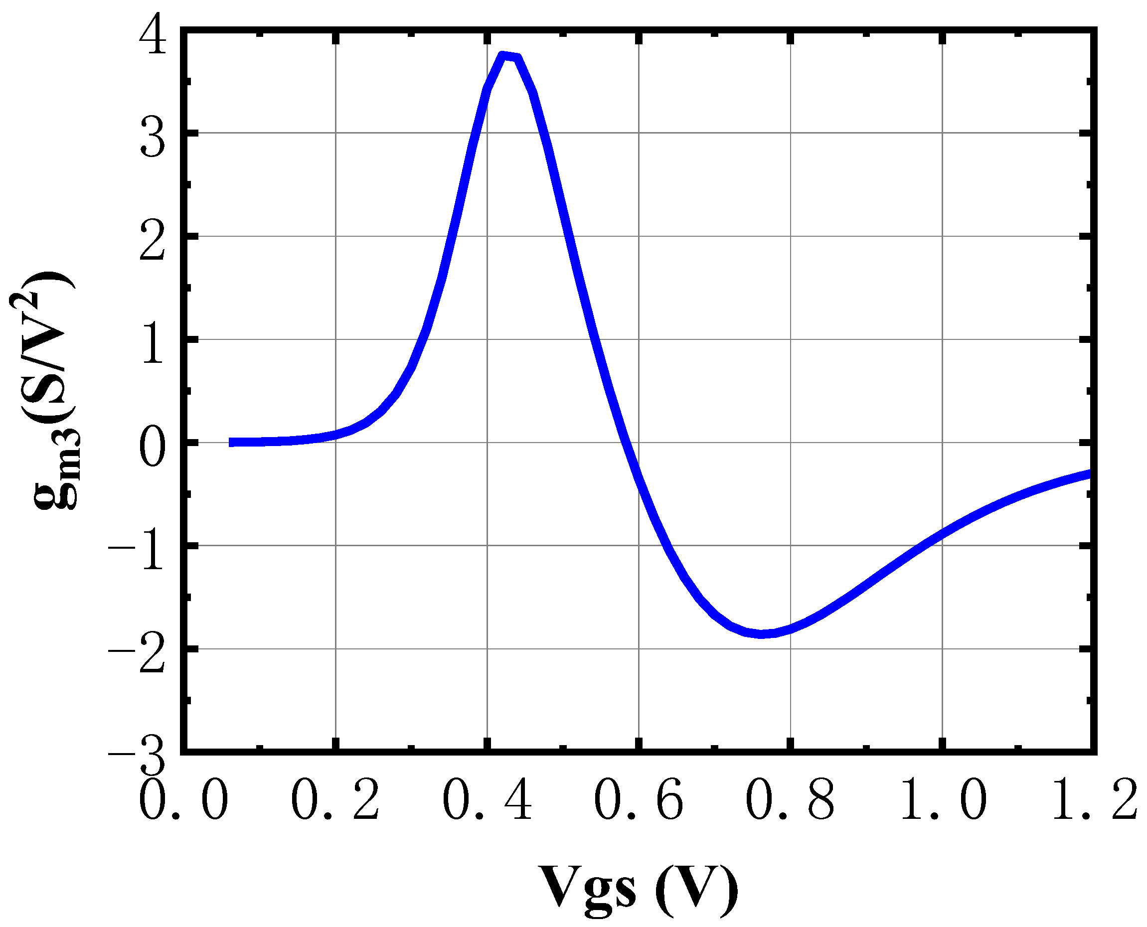
where ω 1 and ω 2 are lower and upper two-tone input frequencies, respectively, and Z L is the frequency-dependent load impedance. It can be seen that the IMD3 of the circuit is highly dependent on the third-order transconductance ( g m 3 ) of the transistor. The third-order transconductance of the transistor exhibits a strong dependence on its bias voltage, as demonstrated in Figure 15. Notably, we can observe that there is a sweet spot for the third-order transconductance, where the IMD3 distortion can be minimized.
To expand the sweet spot range of the third-order transconductance across the expected power range, this work divides the power cell into two sections, each with different bias voltages. By compensating for the nonlinear components produced by each power cell operating under different bias conditions, the overall power amplifier achieves a low IMD3 distortion. Figure 16 compares the IMD3 performance of the circuit with and without using MGTR. It can be seen that after adopting MGTR technology, the circuit’s IMD3 distortion can be effectively suppressed by choosing an appropriate combination of different bias voltages.

3.2. The Integrated Bias Circuit

The linearity of the power amplifier is closely related to its bias voltage. CMOS integrated bias circuits can be employed to optimize the power amplifier’s linearity, which is one of the advantages of CMOS technology. Additionally, the implementation of an integrated bias circuit eliminates the necessity for ESD protection circuits due to external bias voltages, thereby improving system integration and simplifying the design.
In this work, the bias voltages of the power amplifier are adjustable and are shown in Figure 17. The common-source transistor voltage can be adjusted within the range of approximately 400 mV to 680 mV, while the common-gate transistor voltage can be tuned between approximately 1.9 V and 2.9 V. By adjusting the bias voltages, it is ensured that under all PVT conditions, the voltage across each power transistor remains within its maximum tolerable limit, thereby ensuring the reliability of the power amplifier and long-term operational stability of the design. Additionally, at different bias voltages, the output impedance of the common gate bias circuit undergoes significant changes. To prevent the impact of output impedance variations on the PA’s linearity, this paper adds a voltage buffer following the adjustable resistor in the common-gate bias circuit (Figure 17b) to stabilize circuit output impedance.

4. Simulation Results

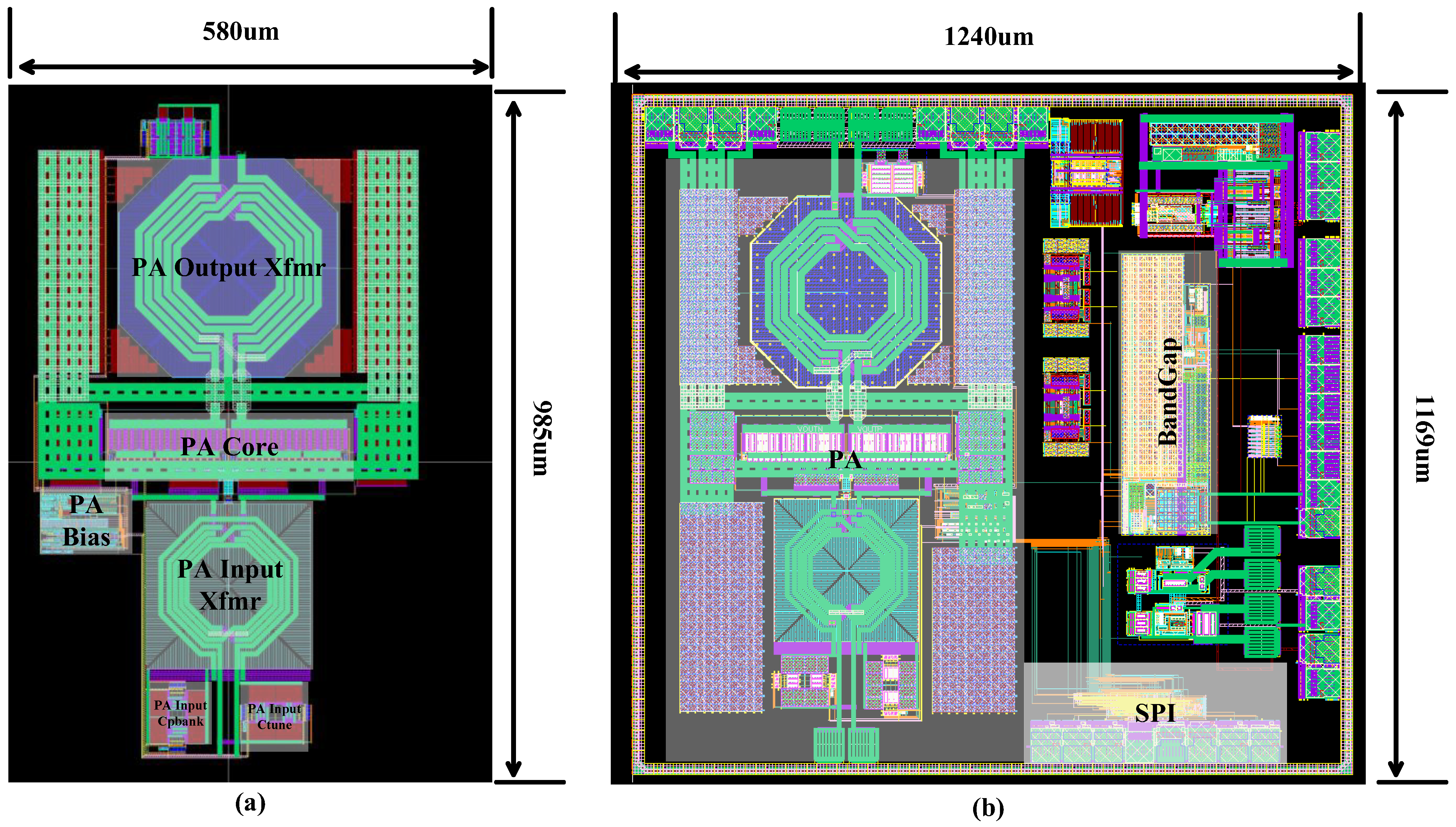
The fully integrated power amplifier in this design is manufactured using the SMIC 55 nm process, with a 3.3 V supply voltage. Occupying an area of 0.57 mm2, as shown in Figure 18a, multiple ground pads are strategically placed to reduce the inductance of the bonding wires. The chip occupies an area of 1.45 mm2, as shown in Figure 18. In addition to the power amplifier, the chip also includes the SPI module, a bandgap, and other test modules. The simulation software used in this design is Cadence IC 617.
The simulated S-parameter results, shown in Figure 19, indicate that the small-signal gain of the PA is approximately 9.46 dB/9.98 dB-11.48 dB at both 2.4 GHz and 5 GHz. Within the 5 GHz frequency range, the gain remains relatively flat across the entire bandwidth.
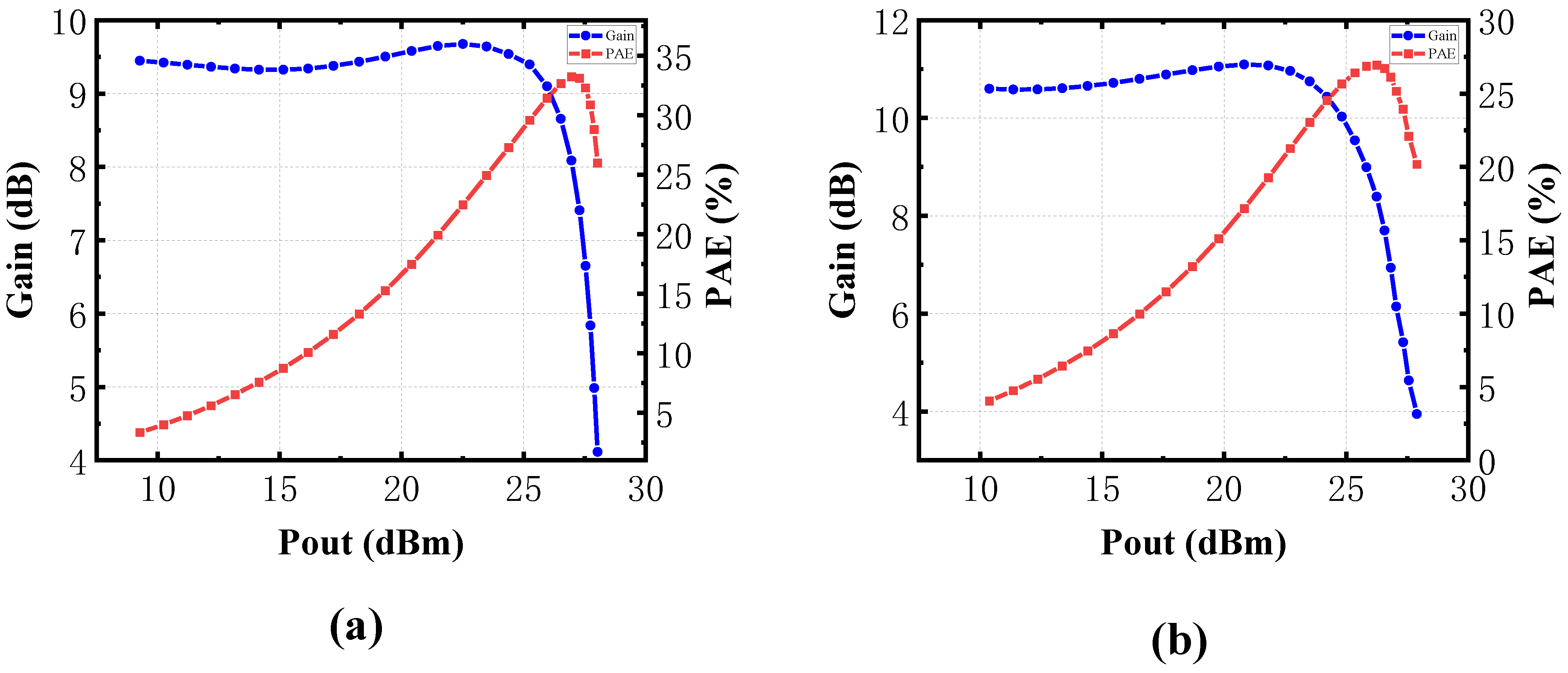
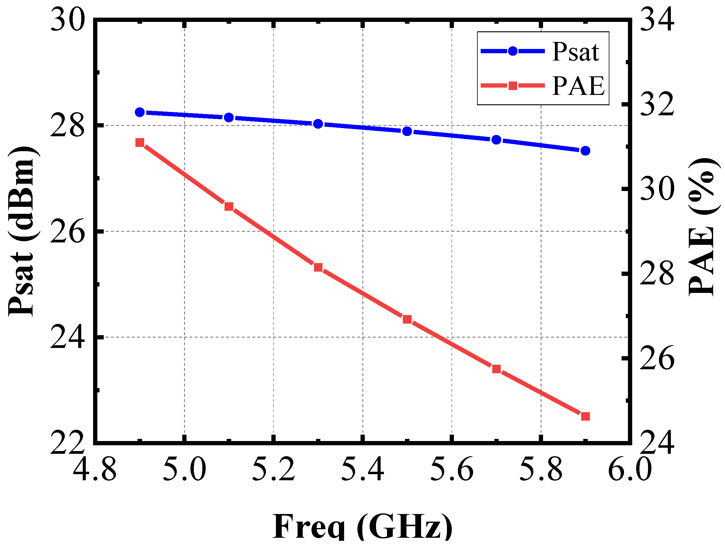
To characterize the linearity and efficiency of the PA, continuous wave simulations were employed. The simulation results displayed in Figure 20 and Figure 21 illustrate the single-tone linearity of the PA. The saturation power, power gain, and power-added efficiency (PAE) are presented in the operating frequency range. It is seen that at 2.4 GHz and 5 GHz, the saturation power is 28.03 dBm/27.5–28.2 dBm, PAE is 33.25/24.5–31.1%, and the power gain is 9.37/11.5–10.03 dB. Additionally, the saturation power of the PA remains above 27.5 dBm.
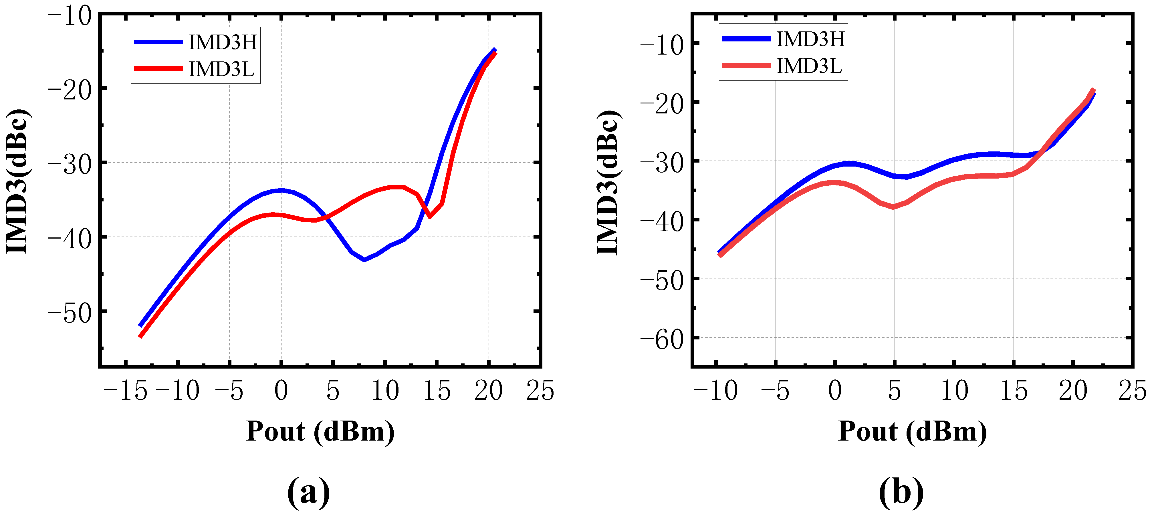
The results for two-tone linearity are depicted in Figure 22. In the 2.4 GHz and 5 GHz frequency bands, the IMD3 is within −30 dBc when the output power is 15 dBm, meeting the requirements of WLAN standards.
Finally, a comparison between the proposed dual-band PA in this study and other PAs is presented in Table 3.

5. Discussion

From the performance summary in Table 3, it is evident that the output power of current dual-band or multi-band power amplifiers is generally insufficient (below 26 dBm). Furthermore, when the distance between high and low frequency bands is significant, both the output power and efficiency in the higher frequency bands tend to decrease. However, the saturated output power of the proposed dual-band power amplifier, achieved using the design methodology proposed in this paper based on the insertion loss optimization of matching networks, is significantly higher than that of current power amplifiers of the same type. Moreover, its efficiency does not show notable degradation, which validates the correctness of the proposed design methodology. This paper addresses the issue of insufficient output power commonly found in current dual-band and multi-band power amplifiers.
In terms of topologies of PAs, both this paper and references [17,28,29,30] employ a linear power amplifier topology biased in Class A or Class AB. In contrast, reference [31] uses a switching power amplifier biased in Class E, which offers a significant efficiency advantage over linear power amplifiers. In terms of occupied area, references [17,29] require a larger area due to the multi-path linear power combining, which, however, offers a significant gain advantage over other power amplifiers. The remaining amplifiers utilize a single-stage amplification structure, resulting in a smaller occupied area but consequently lower gain. In summary, the proposed dual-band power amplifier has a compact footprint and demonstrates a distinct advantage in output power. Additionally, it achieves a favorable trade-off between gain and efficiency, making it well-suited for dual-band IEEE 802.11ax applications.
To continuously boost data throughput, WLAN standards are progressively increasing bandwidth, optimizing spectral efficiency, and adopting more complicated modulation schemes, which pose more stringent linearity and efficiency requirements on power amplifiers. The future research focus for power amplifiers in WLAN applications may aim at improving linearity and efficiency at power back-off levels while meeting high linearity requirements in broadband or multi-band switching conditions

6. Conclusions

This paper presents a dual-band fully integrated high linearity CMOS power amplifier (PA). To deliver high output power, a design methodology for a dual-band matching network is proposed. Based on the proposed methodology, reconfigurable dual-band matching networks are implemented. Furthermore, the proposed input dual-band matching network employs a reconfigurable transformer to achieve a low reflection coefficient across both bands, and the principle of the reconfigurable transformer is thoroughly studied. The simulation results validate the PA’s dual-band operation. For continuous-wave operation, the PA achieves saturated powers ( P s a t ) of 28.03 dBm and 27.5–28.2 dBm, with power added efficiencies (PAE) of 33.2% and 24.6–31.1%, in the2.4 GHz and 5 GHz WLAN bands, respectively. Compared with other dual-band or multi-band PAs, the PA demonstrates a superior performance in output power. According to the simulation results, the proposed PA shows great potential for WLAN applications.

Author Contributions

Conceptualization, H.S. and B.W.; data curation, H.S.; formal analysis, H.S.; investigation, H.S.; methodology, H.S. and B.W.; resources, B.W.; supervision, B.W.; validation, H.S. and B.W.; writing—original draft, H.S. All authors have read and agreed to the published version of the manuscript.

Funding

This work is supported by the Hangzhou Science and Technology Development Program. (No: 2024SZD1A40).

Institutional Review Board Statement

Not applicable.

Informed Consent Statement

Not applicable.

Data Availability Statement

The data in this paper are all from simulation and test results of real circuits, and there is no data plagiarism or falsification. Due to project confidentiality requirements, we regret that we cannot release more details of the data at this time.

Conflicts of Interest

Bin Wu was employed by Zhejiang CASEMIC Electronics Technology Co., Ltd. The remaining authors declare that the research was conducted in the absence of any commercial or financial re-lationships that could be construed as a potential conflict of interest.

References

  1. Kim, W.; Seok, H.G.; Lee, G.; Kim, S.; Lee, J.K.; Kim, C.; Kim, J. A Fully Integrated IEEE 802.15.4/4z-Compliant UWB System-on-Chip RF Transceiver Supporting Precision Positioning in a CMOS 28-nm Process. IEEE J. Solid-State Circuits 2023, 58, 3408–3420. [Google Scholar] [CrossRef]
  2. Lee, J.; Han, J.; Lo, C.L.; Lee, J.; Kim, W.; Kim, S.; Kang, I. NB-IoT and GNSS All-In-One System-On-Chip Integrating RF Transceiver, 23-dBm CMOS Power Amplifier, Power Management Unit, and Clock Management System for Low Cost Solution. IEEE J. Solid-State Circuits 2020, 55, 3400–3413. [Google Scholar] [CrossRef]
  3. Kim, N.-S. A Digital-Intensive Extended-Range Dual-Mode BLE5.0 and IEEE802.15.4 Transceiver SoC. IEEE Trans. Microw. Theory Tech. 2020, 68, 2020–2029. [Google Scholar] [CrossRef]
  4. Wang, D.; Liu, Z.; Tan, Y.; Xu, C.; Li, H.; Jiang, H.; Liao, H. A 2.85-mm2 Wideband RF Transceiver in 40-nm CMOS for IoT Micro-Hub Applications. IEEE Trans. Circuits Syst. I Regul. Pap. 2023, 70, 3930–3943. [Google Scholar] [CrossRef]
  5. Duan, Z.; Fang, Y.; Zhu, H.; Wu, B.; Wang, Y.; Dai, Y.; Gao, H. A S-band switchless bi-directional transceiver with a 52% fractional bandwidth in CMOS technology. Microelectron. J. 2023, 143, 106036. [Google Scholar] [CrossRef]
  6. Andersen, N.; Bagga, S.; Michaelsen, J.A.; Hjortland, H.A.; Leene, L.; Skår, T.; Wisland, D.T. 4.1 A 79.7μW Two-Transceiver Direct-RF 7.875GHz UWB Radar SoC in 40nm CMOS. In Proceedings of the IEEE International Solid-State Circuits Conference (ISSCC), San Francisco, CA, USA, 18–22 February 2024; pp. 76–78. [Google Scholar] [CrossRef]
  7. Lu, C.; Chen, S.L.; Liu, J.; Bao, J.; Wang, Y.; Zhao, Y. Dual-Band 802.11ax Transceiver Design With 1024-QAM and 160-MHz CBW Support. IEEE Solid-State Circuits Lett. 2023, 6, 137–140. [Google Scholar] [CrossRef]
  8. Lu, E.; Li, W.K.; Deng, Z.; Rostami, E.; Wu, P.A.; Chang, K.M.; Shanaa, O. 10.4 A 4×4 Dual-Band Dual-Concurrent WiFi 802.11ax Transceiver with Integrated LNA, PA and T/R Switch Achieving +20dBm 1024-QAM MCS11 P out and −43dB EVM Floor in 55nm CMOS. In Proceedings of the IEEE Solid-state Circuits Conference Digest of Technical Papers, San Francisco, CA, USA, 16–20 February 2020. [Google Scholar] [CrossRef]
  9. Lee, J.; Jang, J.; Lee, W.; Suh, B.; Yoo, H.; Park, B.; Yoo, S. 4.2 A Tri-Band Dual-Concurrent Wi-Fi 802.11be Transceiver Achieving -46dB TX/RX EVM Floor at 7.1GHz for a 4K-QAM 320MHz Signal. In Proceedings of the IEEE International Solid-State Circuits Conference (ISSCC), San Francisco, CA, USA, 18–22 February 2024. [Google Scholar] [CrossRef]
  10. Ben-Bassat, A.; Gross, S.; Lane, A.; Nazimov, A.; Khamaisi, B.; Solomon, E.; Degani, O. A Fully Integrated 27dBm Dual-Band All-Digital Polar Transmitter Supporting 160MHz for WiFi 6 Applications. IEEE Solid-State Circuits 2020, 55, 3414–3425. [Google Scholar] [CrossRef]
  11. Khamaisi, B.; Ben-Haim, D.; Nazimov, A.; Ben-Bassat, A.; Gross, S.; Shay, N.; Degani, O. A 16nm, +28dBm Dual-Band All-Digital Polar Transmitter Based on 4-core Digital PA for Wi-Fi6E Applications. In Proceedings of the IEEE Solid-state Circuits Conference Digest of Technical Papers, San Francisco, CA, USA, 20–26 February 2022. [Google Scholar] [CrossRef]
  12. Li, S.; Su, G.; Wang, X.; Liu, J. A 8–12 GHz power amplifier with high out-of-band rejection. Microelectron. J. 2024, 144, 106084. [Google Scholar] [CrossRef]
  13. Nikandish, G.R.; Staszewski, R.B.; Zhu, A. Broadband fully integrated GaN power amplifier with minmum-inductance BPF matching and two-transistors AM-PM compensation. IEEE Trans. Circuits Syst. I Regul. Pap. 2020, 67, 4211–4223. [Google Scholar] [CrossRef]
  14. Liu, B.; Boon, C.C.; Mao, M.; Choi, P.; Guo, T. A 2.4–6 GHz Broadband GaN Power Amplifier for 802.11ax Application. IEEE Trans. Circuits Syst. I Regul. Pap. 2021, 68, 2404–2417. [Google Scholar] [CrossRef]
  15. Nikandish, G.R.; Nasri, A.; Yousefi, A.; Zhu, A.; Staszewski, R.B. A Broadband Fully Integrated Power Amplifier Using Waveform Shaping Multi-Resonance Harmonic Matching Network. IEEE Trans. Circuits Syst. I Regul. Pap. 2021, 69, 2–15. [Google Scholar] [CrossRef]
  16. Meng, X.; Yu, C.; Liu, Y.; Wu, Y. Design approach for implementation of class-J broadband power amplifiers using synthesized band-pass and low pass matching topology. IEEE Trans. Microw. Theory Tech. 2017, 65, 4984–4996. [Google Scholar] [CrossRef]
  17. Liu, B.; Zhou, R.; Zhu, Z. Reconfigurable 2.4/5.0-GHz Dual-Band CMOS Power Amplifier for WLAN 802.11ax. IEEE Trans. Circuits Syst. I Regul. Pap. 2024, 71, 3120–3133. [Google Scholar] [CrossRef]
  18. Lee, J.; Paek, J.S.; Hong, S. Millimeter-Wave Frequency Reconfigurable Dual-Band CMOS Power Amplifier for 5G Communication Radios. IEEE Trans. Microw. Theory Tech. 2021, 70, 801–812. [Google Scholar] [CrossRef]
  19. Ko, J.; Nam, S. A two-stage S-/X-band CMOS power amplifier for high-resolution radar transceivers. IEEE Microw. Wirel. Compon. Lett. 2018, 28, 606–608. [Google Scholar] [CrossRef]
  20. Lee, M.; Park, C. A Triple-Band CMOS Power Amplifier Using Multi-Band and Switchable Matching Network for Wireless Mobile. IEEE Trans. Microw. Theory Tech. 2019, 67, 4220–4231. [Google Scholar] [CrossRef]
  21. Choi, H.W.; Choi, S.; Kim, C.Y. A 25-GHz Power Amplifier Using Three-Stage Antiphase Linearization in Bulk 65-nm CMOS Technology. IEEE Microw. Wirel. Compon. Lett. 2020, 30, 489–491. [Google Scholar] [CrossRef]
  22. Lee, W.; Yoo, J.; Hong, S. A 28-GHz CMOS Power Amplifier Linearized by Dynamic Conductance Control and Body Carrier Injection. IEEE Microw. Wirel. Compon. Lett. 2021, 31, 1071–1074. [Google Scholar] [CrossRef]
  23. Rawat, A.S.; Rajendran, J.; Mariappan, S.; Shasidharan, P.; Kumar, N.; Yarman, B.S. A 919 MHz—923 MHz, 21 dBm CMOS Power Amplifier with Bias Modulation Linearization Technique Achieving PAE of 29% for LoRa Application. IEEE Access 2022, 10, 79365–79378. [Google Scholar] [CrossRef]
  24. Joo, T.; Koo, B.; Hong, S. A WLAN RF CMOS PA with large-signal MGTR method. IEEE Trans. Microw. Theory Tech. 2013, 61, 1272–1279. [Google Scholar] [CrossRef]
  25. Pozar, D.M. Microwave Engineering; Wiley: Hoboken, NJ, USA, 2006. [Google Scholar]
  26. Trinh, V.S.; Park, J.D. Theory and Design of Impedance Matching Network Utilizing a Lossy On-Chip Transformer. IEEE Access 2019, 7, 140980–140989. [Google Scholar] [CrossRef]
  27. Yoon, Y.; Kim, H.; Park, Y.; Ahn, M.; Lee, C.H.; Laskar, J. A high power and highly linear CMOS switched capacitor. IEEE Microw. Wirel. Compon. Lett. 2010, 20, 619–621. [Google Scholar] [CrossRef]
  28. Liu, B.; Quan, X.; Boon, C.C.; Khanna, D.; Choi, P.; Yi, X. Reconfigurable 2.4-/5-GHz Dual-Band Transmitter Front-End Supporting 1024-QAM for WLAN 802.11ax Application in 40-nm CMOS. IEEE Trans. Microw. Theory Tech. 2020, 68, 4018–4030. [Google Scholar] [CrossRef]
  29. Singh, R.; Paramesh, J. A digitally-tuned triple-band transformer power combiner for CMOS power amplifiers. In Proceeding of the IEEE Radio Frequency Integrated Circuits Symposium, Honolulu, HI, USA, 4–6 June 2017; pp. 332–335. [Google Scholar] [CrossRef]
  30. Zhai, C.; Liu, H.Y.; Cheng, K.K.M. Single-Chip CMOS Reconfigurable Dual Band Tri-Mode High-Efficiency RF Amplifier Design. IEEE Trans. Circuits Syst. II Express Briefs 2020, 68, 868–872. [Google Scholar] [CrossRef]
  31. Lin, W.J.; Huang, P.S.; Cheng, J.H.; Tsai, J.H.; Alsuraisry, H.; Huang, T.W. A dual-band class-E power amplifier with concurrent matching network in 0.18-mu m CMOS. Microw. Opt. Technol. Lett. 2018, 60, 1672–1675. [Google Scholar] [CrossRef]
Figure 1. Simplified schematic of output matching circuit.
Applsci 14 10768 g001
Figure 2. Simulated power contours and PAE contours in 2.4 and 5 GHz bands. (a) 2.4 GHz. (b) 5.5 GHz.
Applsci 14 10768 g002
Figure 3. Reflection coefficient contours of output matching network. (a) 2.45 G. (b) 5.5 G.
Applsci 14 10768 g003
Figure 4. Insertion loss contours of output matching network. (a) 2.4 G. (b) 5.5 G.
Applsci 14 10768 g004
Figure 5. Layout of output transformer.
Applsci 14 10768 g005
Figure 6. On-resistance and Coff of switch transistor versus size.
Applsci 14 10768 g006
Figure 7. Achieved insertion loss of the output matching network. (a) 2.4 GHz. (b) 5 GHz.
Applsci 14 10768 g007
Figure 8. Reconfigurable input matching circuit.
Applsci 14 10768 g008
Figure 9. Simplified schematic of the reconfigurable transformer.
Applsci 14 10768 g009
Figure 10. Simplified schematic of the tunable inductor.
Applsci 14 10768 g010
Figure 11. (a) Equivalent inductance and quality factor versus C t . (b) Equivalent quality factor versus R t .
Applsci 14 10768 g011
Figure 12. The layout of the reconfigurable transformer.
Applsci 14 10768 g012
Figure 13. S-parameter comparison with fixed transformer. (a) Same C i n p . (b) Larger C i n p in fixed transformer.
Applsci 14 10768 g013
Figure 15. g m 3 vs. gate voltage.
Applsci 14 10768 g015
Figure 16. Comparison of IMD3 with and without MGTR.
Applsci 14 10768 g016
Figure 17. Schematic of integrated circuits. (a) Common source. (b) Common gate.
Applsci 14 10768 g017
Figure 18. (a) Layout of proposed PA. (b) Layout of test chip.
Applsci 14 10768 g018
Figure 19. Simulated S-parameters. (a) 2.4 G band. (b) 5 G band.
Applsci 14 10768 g019
Figure 20. Simulated power gain and PAE versus output power. At (a) 2.4 and (b) 5.5 GHz modes.
Applsci 14 10768 g020
Figure 21. Simulated P s a t and PAE at different frequencies.
Applsci 14 10768 g021
Figure 22. Simulated IMD3 versus output. At (a) 2.4 and (b) 5.5 GHz modes.
Applsci 14 10768 g022
Table 1. Parameter of output transformer.
InductanceQuality Factor (Q)Coupling Coefficient (k)
L p 1.49 nH16.330.75
L s 2.83 nH19.39
Table 2. Parameters of reconfigurable transformer.
SW-OffSW-On
L p 1.03 nH L p 1.15 nH
Q p 8.39 Q p 7.55
L s 877.15 pH L s 936.65 pH
Q s 9.56 Q s 9.21
k0.76k0.77
Table 3. Comparison with other dual-band PAs.
This Work ***[17] **[28] **[29] **[30] **[31] **
Freq (GHz)2.4/4.9–5.92.4/5–62.4/4.9–5.92.5/3/3.51.8/2.62.4/5
Bandwidth (−3 dB)2.06–3.04/3.15–6.62.1–2.8/4–6 *2.2–3.2/3.8–6.5 *2.2–2.8/2.8–3.6/3.1–4.1 *N. A2–5 *
Gain (dB)9.45/11.48–10.0314/18–169.2/11.3–11.9~1510–11 *12.3/8.4
P s a t (dBm)28.03/27.5–28.225.4/24.4–24.823/21.9–22.422.5/21.526.2/23.121.5/21.4
PAE (%)33.25/24.6–31.125/20.8–27.327/24.2–28.216.5/15(DE)32.2/31.838.4/31
VDD (V)3.32.52.51.23.33.6
Chip   Area   ( mm 2 ) 0.571.140.722.971.40.5
Technology55 nm40 nm40 nm65 nm0.35 µm0.18 µm
* Graphically estimated; ** measurement results; *** post-layout simulation results.
Disclaimer/Publisher’s Note: The statements, opinions and data contained in all publications are solely those of the individual author(s) and contributor(s) and not of MDPI and/or the editor(s). MDPI and/or the editor(s) disclaim responsibility for any injury to people or property resulting from any ideas, methods, instructions or products referred to in the content.