Article

Assessment of Dielectric Strength for 3D Printed Solid Materials in Terms of Insulation Coordination

by
Cihat Cagdas Uydur
Technical Sciences Vocational School, Trakya University, Edirne 22030, Türkiye
Appl. Sci. 2024, 14(24), 11860; https://doi.org/10.3390/app142411860
Submission received: 8 November 2024 / Revised: 5 December 2024 / Accepted: 17 December 2024 / Published: 18 December 2024
(This article belongs to the Special Issue Advances in Electrical Insulation Systems)

Abstract

:
Insulating materials can be classified into solid, liquid, and gaseous forms. Solid insulation materials are divided into different types such as organic, inorganic, and polymer types. In electrical circuits, solid insulation materials are generally used as components that provide insulation and mechanical support. In recent years, as a result of developing technologies, the production of participation insulation materials with 3D printing technology has become widespread. Three-dimensional printing technology enables the rapid creation of objects by combining materials based on digital model data. It is important to evaluate the materials produced with 3D printing in terms of insulation coordination. Studies have shown that the electrical breakdown strength of solid dielectrics varies depending on factors such as sample type, thickness, the magnitude of applied voltage, and the temperature of the physical environment. According to IEC-60243 standards, there are various methods to measure the breakdown strength of solid insulators applied to different voltage types. In this study, the behavior of PLA, ABS, ASA, PETG, and PC/ABS materials produced with 3D printing and having the potential to be used as insulation materials when exposed to high voltage within the scope of insulation coordination was investigated. The breakdown strengths of solid insulation materials produced with 3D printing were measured in the high-voltage laboratory within the scope of IEC-60243. Breakdown strength was statistically evaluated with the Weibull distribution. Damage analysis of the breakdowns in the test specimens was examined in detail with ImageJ software. With the comparative analysis, the behaviors of PLA, ABS, ASA, PETG, and PC/ABS solid insulation materials were revealed and their superiority over each other was determined.

1. Introduction

Materials used in electricity are classified as conductors, insulators, and semiconductors. All elements with eight or more electrons in the outer orbits of their atoms are called insulators. Insulator materials are found in solid, liquid, and gaseous forms. Solid insulator materials are classified as organic, inorganic, and polymer insulators [1]. The behavior of insulating materials under operating conditions is an important feature to be considered in low-voltage and high-voltage applications [2,3,4]. In electrical circuits, solid insulators are frequently utilized as components to offer insulation, mechanical support, and to keep conductors separated [5,6]. However, in high-voltage applications like electrical installations and power grid transmission, the electric field distribution across the surface of solid insulators often becomes highly non-uniform. This is especially true in three-phase connections, where the maximum electric field strength (Emax) can result in charge accumulation or partial discharge [5,7]. In such high-voltage applications, insulation is the most critical element to be considered, as is the applied voltage value [7,8]. In this context, insulation coordination is the mutual compatibility of various insulation levels and protection levels in order to avoid the damage caused by overvoltages. A significant proportion of faults occurring in power systems are due to insulation problems.
With developing technology, on-site and instant production has become possible. An advantage of this situation is that insulation materials can also be produced with the help of this technology. Rapid prototyping is commonly known as three-dimensional (3D) printing [9]. Three-dimensional printing technology is a tool that rapidly creates objects by layering materials according to digital model data, achieving this through a continuous process of layer-by-layer stacking and printing [10]. The first additive manufacturing process was developed by Charles W. Hull in 1986. Three-dimensional printing is favored for producing functional prototypes and small batches due to its rapid production capability. Moreover, certain geometric features of objects can only be achieved through additive manufacturing [11]. Three-dimensional printing technology is increasingly being incorporated into and integrated with various industries and fields [12]. This technology reduces material waste in the production of complex parts, the creation of innovative electronic devices, industrial design, model manufacturing, architectural design, jewelry, toys, ceramics, the aerospace, education, clothing industries, and medical fields, making it a valuable tool for various industries [9,13,14,15,16,17]. Three-dimensional printing technology is affected by printer cost, the raw materials used, structure, and performance [18]. It is very important to evaluate the insulation coordination in the insulating materials produced with 3D printing technology. It is necessary to examine the faults that may occur in the dielectric material and to reveal its characteristics by analyzing the material behavior [19].
Research on dielectric breakdown mechanisms has been ongoing for years in terms of theoretical and experimental studies [20,21,22,23]. Considering the reliable operation of devices and high-voltage equipment needed in the electrical and electronics industry, failures of insulation materials due to aging and wear are inevitable. Experimentally, it has been observed that the strength of solid insulation materials to electrical breakdowns varies depending on the type of material, dimensions, and applied voltage [24]. In addition, it has been emphasized in studies that factors such as ambient temperature and humidity, which determine the working conditions, should also be taken into account [25]. There are various methods for determining the breakdown strength of solid insulating materials. These methods have applications for different voltage types by IEC-60243 and IEC-60060 standards [26,27]. These are the “Short-time (rapid-rise) test” in the 10th section of IEC 60243-1, the “20 s step-by-step test” in IEC 60243-1, the “Slow rate-of-rise test” in the relevant section of IEC 60243-1, and the Multi-Level Method, in IEC 60060 [28].
In recent years, the interest in 3D printed materials has increased due to their potential to transform the electrical and electronics industry. Conductive and insulating materials produced with 3D printing allow for the creation of materials and devices with the properties required by the industry. In this context, 3D printing (3DP) technologies accelerate prototyping and facilitate the creation of complex shapes and geometries that are difficult to achieve with traditional manufacturing methods [9]. Multilayer or additive manufacturing technologies have begun to be used as technologies that offer new possibilities for producing customized equipment that is tailored to needs, including conductive and insulating materials. In addition to analyzing numerical values to interpret breakdown voltage or breakdown strength measurements, image processing and inspection technologies have also become increasingly common in recent years.
The term image classification simply refers to the process of identifying an unknown object within an image as belonging to a particular group from a set of possible object groups [29]. The field of image processing, in a broad sense, deals with the processing of data that are two-dimensional in nature. Image processing techniques find applications in many areas, especially image enhancement, pictorial image recognition, and the efficient coding of images for transmission or storage [30]. Computer image processing-based methods are being investigated as an alternative to provide solutions for practical measurement, identification, and size distribution analysis [31]. Imaging technology is progressing rapidly, making imaging more affordable, faster, and more sensitive, which drives the need for advanced image processing and analysis techniques. A variety of software is available, ranging from commercial to academic and specialized applications, but accessibility is the most crucial feature for scientific research software. Open-source software is particularly well-suited for scientific studies because it allows for free examination and modification. The open-source platform ImageJ is widely used for this reason, as it is freely accessible [32]. It also runs on major operating systems on the market and is also an open-source image analysis software for processing materials [32]. ImageJ is highly useful for calculating the area, perimeter, or shape of solid objects with defined boundaries [33]. The software allows for a detailed examination of area ratios for different colors within images.
In this study, the behavior of solid insulation materials, which can be fabricated using 3D printing technology, was analyzed under high-voltage conditions within the framework of insulation coordination. In this context, PLA, ABS, ASA, PETG, and PC/ABS materials, which are currently used or have potential for use as electrical insulation, were selected. The breakdown strengths of solid insulation materials produced with 3D printing were measured in a high-voltage laboratory within the scope of IEC-60243. The Weibull distribution of the results obtained from the breakdown strength tests was analyzed. The damage analysis of the breakdowns occurring in the test specimens was evaluated in detail with ImageJ software. With the comparative analysis, the behavior of PLA, ABS, ASA, PETG, and PC/ABS solid insulation materials was revealed and their superiority over each other was determined. The results obtained within the scope of the study were presented in terms of 3D printing and breakdown strength parameters of the materials.

2. Materials and Methods

In this section, the properties of the solid insulation materials used in the study, the 3D printing method, and the usage parameter information of the 3D printings are shared. In addition, the method used in the breakdown strength measurement and the experimental test setup information used in the high-voltage laboratory are presented.

2.1. Solid Insulating Materials

There are many filaments available in different materials, colors, and properties for use in 3D printers. The most commonly used filaments in 3D printers are poly-lactic acid (PLA), acrylonitrile butadiene styrene (ABS), polyethylene terephthalate glycol (PETG), thermoplastic polyurethane (TPU), and nylon filaments. Users prefer different filaments for different working conditions and different working environments from these and existing commercial filaments [16]. PLA, ABS, PETG, acrylonitrile styrene acrylate (ASA) and polycarbonate (PC)/ABS filaments, which have higher electrical insulation properties compared to other available filaments in the working environment, were preferred in the production of samples used in this experimental study. Physical, mechanical, thermal, and electrical properties of the filaments are given in Table 1.

2.2. Three-DimensionalPrinting Method

In order to produce the samples used in the experimental studies, a Qidi Tech brand Q1 Pro type closed and heated cabin FDM technology high-speed 3D printer, the technical specifications of which are given in Table 2, was used. The 3D printer is shown in Figure 1.

2.3. Measurement Method and Experimental Setup

There are various methods for determining the breakdown strength of solid insulating materials. The following methods are suggested for different voltage types by the IEC-60243 and IEC-60060 standards [26,27,36,37,38]: if the breakdown strength of the insulating materials to be tested shows relatively low voltage, there is no harm in applying the test methods mentioned in this section in air. However, if voltage levels where surface discharge will be severe are to be reached, the relevant breakdown strength tests should be performed in environments with stronger insulation properties such as mineral oil, silicone fluid, or ester fluids [39,40,41].
In the method called “Short-time (rapid-rise) test” in section 10 of IEC 60243-1, the test voltage is increased from zero to the insulating material at speeds of 100 V/s, 200 V/s, 500 V/s, 1000 V/s, 2000 V/s, 5000 V/s, etc. The 500 V/s speed among these rising speeds is the most widely preferred rising speed in determining the breakdown strength of different types of materials.
Breakdown tests were carried out in a polymethyl methacrylate (plexiglass) test container with dimensions of 200 × 200 × 200 mm. The test container is shown in Figure 2. The cylinder–cylinder electrode arrangement in the test electrodes is a system consisting of identical cylinder electrodes with rounded corners of a 3 mm radius, 25 mm diameter, and 25 mm height, as mentioned in the IEC 60243-1 standard.
An AC voltage source with a capacity of 90 kV was used to apply voltage to the insulating materials, with rise rates set at 500 V/s. To prevent surface discharges, the electrodes and test sample were submerged in Nytro Lyra X mineral oil within the test container. The connection diagram used for the tests is presented in Figure 3.

3. Results

This section presents the parameters of the test samples produced through 3D printing, the outcomes of the simulation study for electric field distribution, and the results of the breakdown strength measurements conducted in the high-voltage laboratory.

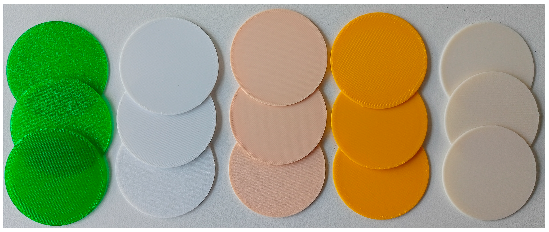
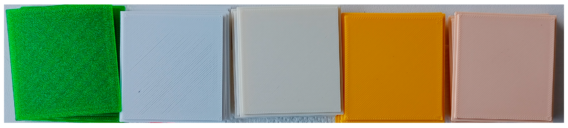
3.1. Specimen Preparation

The samples were first drawn in a CAD program and saved in a file format with an .stl extension. Then, the stl files of the samples were opened in the QIDIStudio slicer program, the printing parameters given in Table 3 were applied, and their .gcodes were obtained. The samples were printed on a 3D printer with the obtained gcodes. Before all sample printing processes, automatic table calibration was performed on the printer, thus ensuring that the dimensional accuracy and print quality of all printed samples were constant.
In order to examine the effect of geometric differences on the 3D printing process, cylindrical and square test samples were printed from each material. Cylindrical test samples are shown in Figure 4 and square test samples are shown in Figure 5. In order to examine the materials in detail, each material was shown in different colors.
PETG material was shown in a transparent green color, PC/ABS material in a white color, PLA material in skin color, ABS material in a yellow color and ASA material in a natural color. Cylindrical test specimens with a diameter of 50 mm and a thickness of 1.2 mm were printed. During printing, it was set to be six layers with a layer height of 0.2 mm and a 100% filling ratio.
The edge length of the square specimens was determined as 50 mm. The test specimens were produced with a thickness of 2.4 mm by setting the 3D printer machine to 12 layers with a layer height of 0.2 and a 100% fill rate.

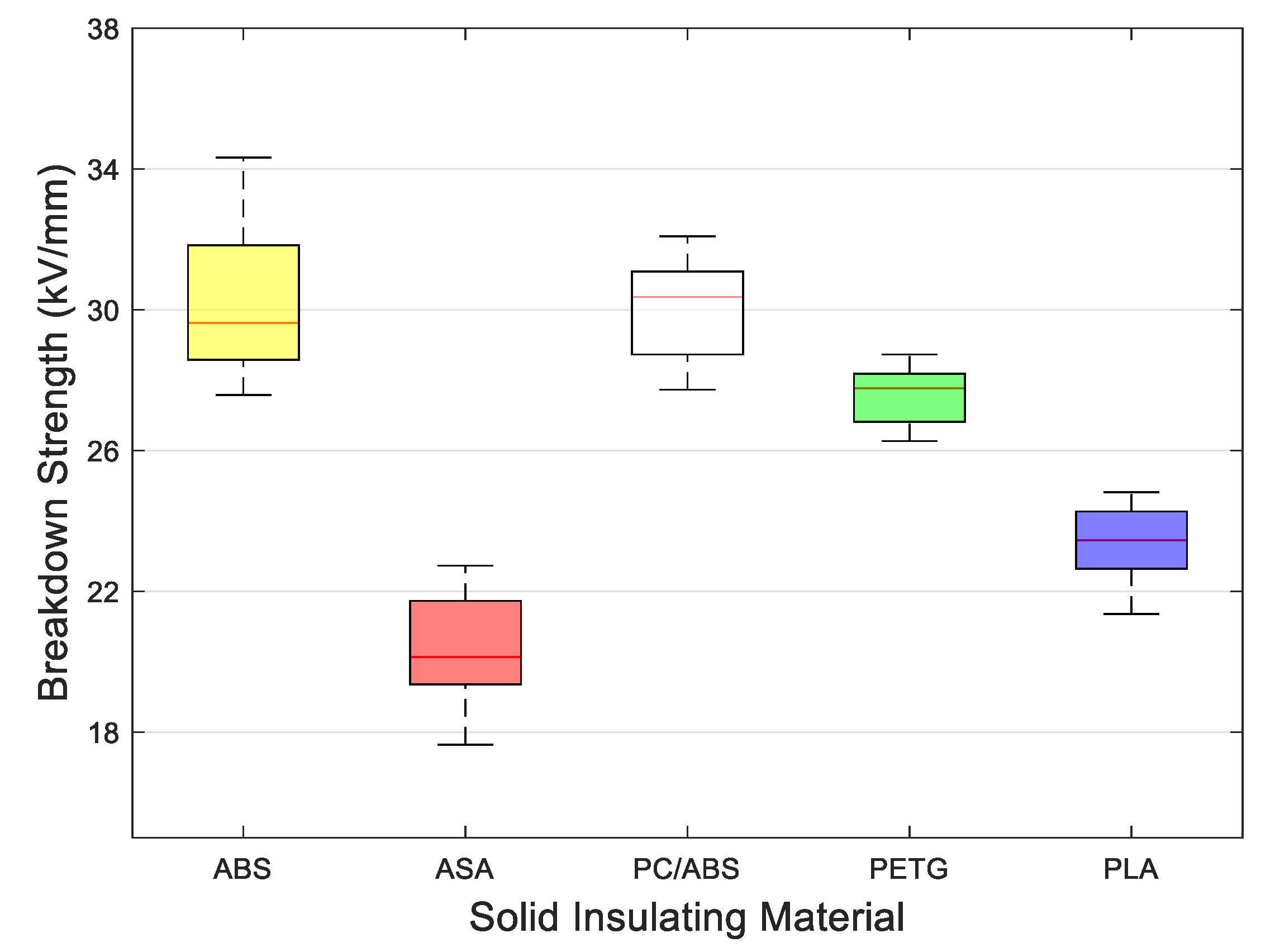
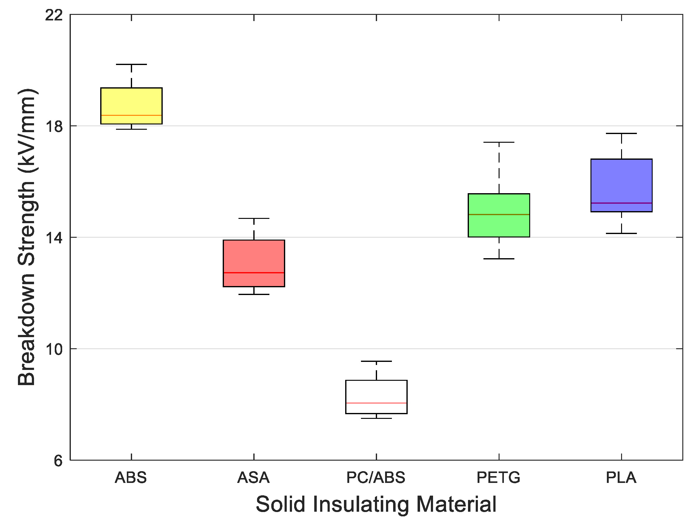
3.2. Results of Breakdown Strength Measurements

To conduct a statistical evaluation of the results obtained from the breakdown strength tests, ten specimens of insulating materials were tested. Prior to testing, the surfaces of the samples were cleaned with ethyl alcohol. The laboratory conditions during the experiments were maintained at a temperature of 25 ± 2 °C, relative humidity of 40 ± 2%, and pressure of 756.8 ± 5 mmHg. The breakdown strength test results of cylindrical specimens are shared in Figure 6, and the breakdown strength test results of square specimens are shared in Figure 7.
Upon examining the results presented in Figure 6, the minimum breakdown strength for the PLA material was recorded at 21.36 kV/mm, while the maximum reached 24.82 kV/mm, resulting in an average breakdown strength of 23.45 kV/mm. For the ABS material, the breakdown strength ranged from 27.58 kV/mm to 34.33 kV/mm, with an average value determined to be 30.28 kV/mm. The ASA material showed an average breakdown strength of 20.35 kV/mm, with a minimum breakdown occurring at 17.64 kV/mm and a maximum of 22.73 kV/mm. The breakdown strength for the PETG material varied between 26.27 kV/mm and 28.73 kV/mm, leading to an average of 27.55 kV/mm. Finally, the PC/ABS material had a minimum breakdown strength of 27.73 kV/mm and a maximum of 32.09 kV/mm, resulting in an average breakdown strength calculated at 30.14 kV/mm.
Analyzing the results for square test specimens displayed in Figure 7, the minimum breakdown strength for the PLA material was recorded at 14.14 kV/mm, with a maximum of 17.73 kV/mm, leading to an average breakdown strength of 15.75 kV/mm. The breakdown strength for the ABS material ranged from 17.88 kV/mm to 20.21 kV/mm, resulting in an average value of 18.73 kV/mm. For the ASA material, the average breakdown strength was measured at 13.06 kV/mm, with a minimum breakdown occurring at 11.95 kV/mm and a maximum of 14.68 kV/mm. The breakdown strength for the PETG material varied between 13.23 kV/mm and 17.41 kV/mm, with an average determined to be 14.94 kV/mm. Lastly, the PC/ABS material exhibited a minimum breakdown strength of 7.50 kV/mm and a maximum of 9.55 kV/mm, culminating in an average breakdown strength calculated at 8.29 kV/mm.
The breakdown strength of the circular PLA material decreased by 32.8%, from 23.45 kV/mm to 15.75 kV/mm. In the ABS material, the circular sample had a breakdown strength value of 30.28 kV/mm, while this value was obtained as 18.73 kV/mm in the square-shaped sample. The rate of change for the ABS material was determined as 38.12%. While a decrease of 35.82% occurred in the ASA material, this rate was calculated as 45.79% in the PETG material. Among the tested material types, the material most affected by the shape change was PC/ABS. While the circular PC/ABS material has a value of 30.14 kV/mm, the square PC/ABS is broken down at a value of 8.29 kV/mm. The change rate is determined as 72.49%. As a result of the breakdown strength measurements made on circular and square-shaped samples, it was observed that square-shaped solid insulator samples were punctured at lower voltages.

4. Discussion

In order to evaluate the results obtained from experimental studies more consistently and in detail, Weibull distribution analysis and image processing methods, which are frequently used in breakdown strength measurements, were used. In this section, the analysis results are shared, and the obtained results are presented in a controversial manner.

4.1. Weibull Analysis

Statistical evaluation of the breakdown strength values obtained for solid insulation materials produced with a 3D printer was performed with the Weibull distribution, as recommended in IEC-62539. Weibull parameters were determined with the White method [42]. The expression of the Weibull cumulative probability function is presented in Equation (1).
F V = 1 e V α β
Here, V represents the breakdown strength to be calculated as probability [kV], α represents the scale parameter [kV] that provides the equality of F = 63.2%, and β represents the shape parameter, which is the slope of the Weibull curve.
In these expressions, the α parameter is the Weibull scale parameter. It represents the characteristic breakdown strength of the dataset obtained from the relevant electrode arrangement and voltage rise rate of the insulating materials. β is the shape parameter and is the slope of the regression curve obtained with the experimental data. It represents the width of the value range that the breakdown strength values will take. Here, statistical distribution analysis was performed for cylindrical insulating material specimens. The data obtained as a result of Weibull distribution analysis are given in Table 4.
When the data in Table 4 are examined, it is observed that the material with the highest characteristic breakdown strength is ABS. The characteristic breakdown strength of ABS was determined as 31.36 kV/mm. PC/ABS came in second with a breakdown strength value of 30.78 kV/mm and PETG came in third. The breakdown strength of the PETG material was 27.92 kV/mm. When we ranked the materials from best to worst in terms of breakdown strength, it turned out to be ABS—PC/ABS—PETG—PLA—ASA. Figure 8 shows the statistical Weibull distribution results for the breakdown strength of materials produced with 3D printing.
When the results in Figure 8 are examined in detail, it is seen that the breakdown strength of the ASA material will be 22 kV/mm with a 95% probability. This situation is determined as 24 kV/mm for the PLA material, 28 kV/mm for the PETG material, 32 kV/mm for the PC/ABS material, and 34 kV/mm for the ABS material.

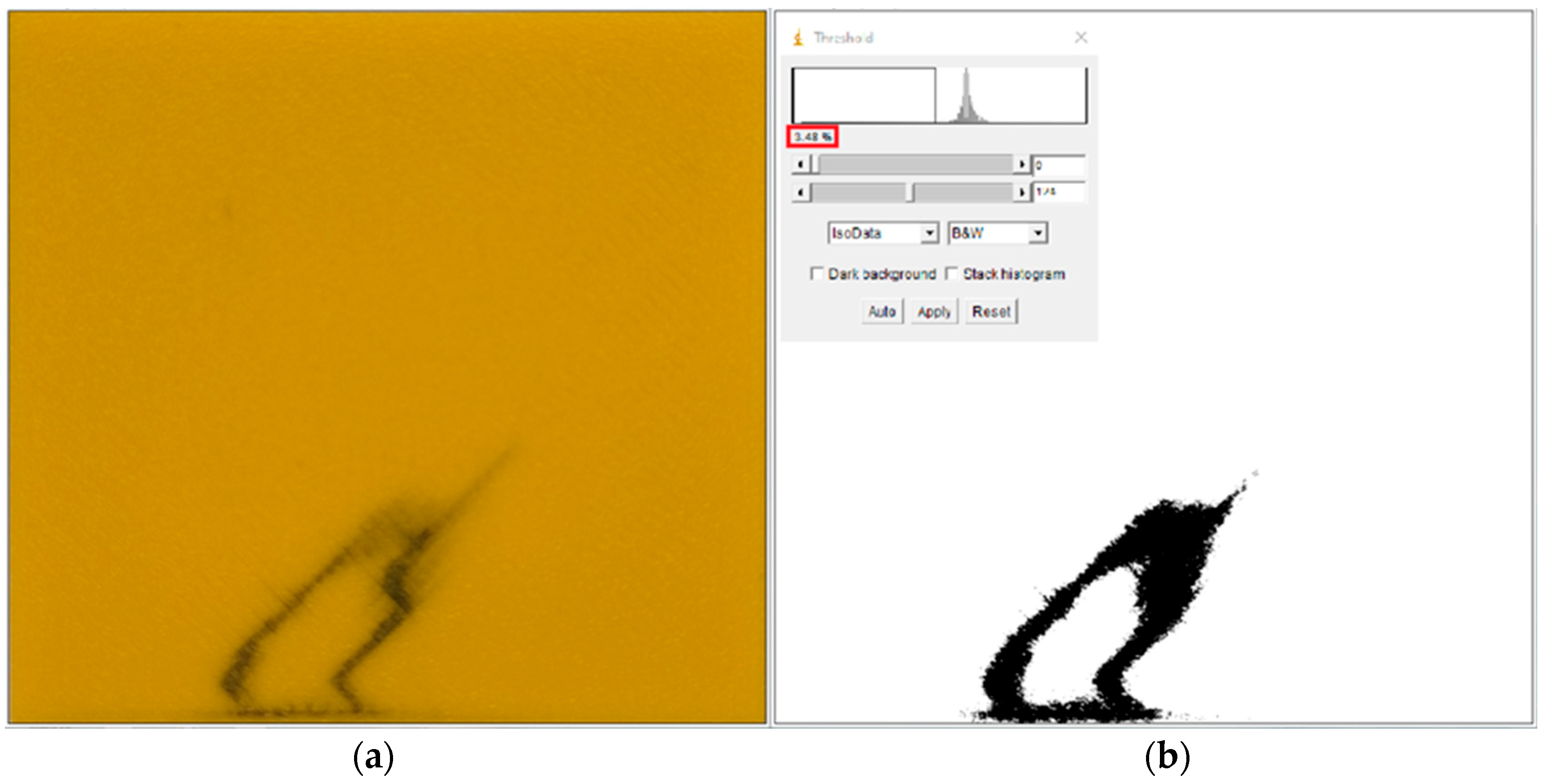
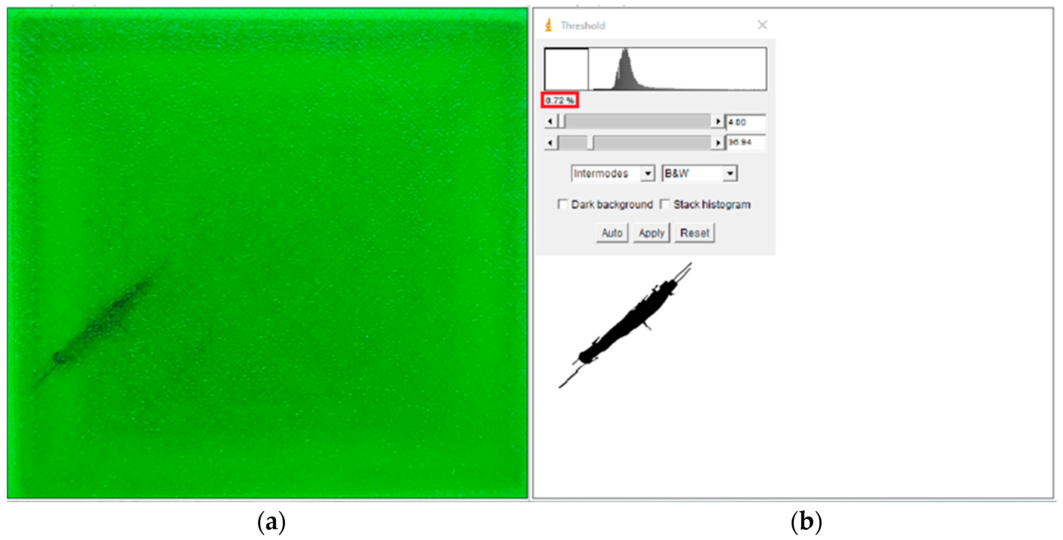
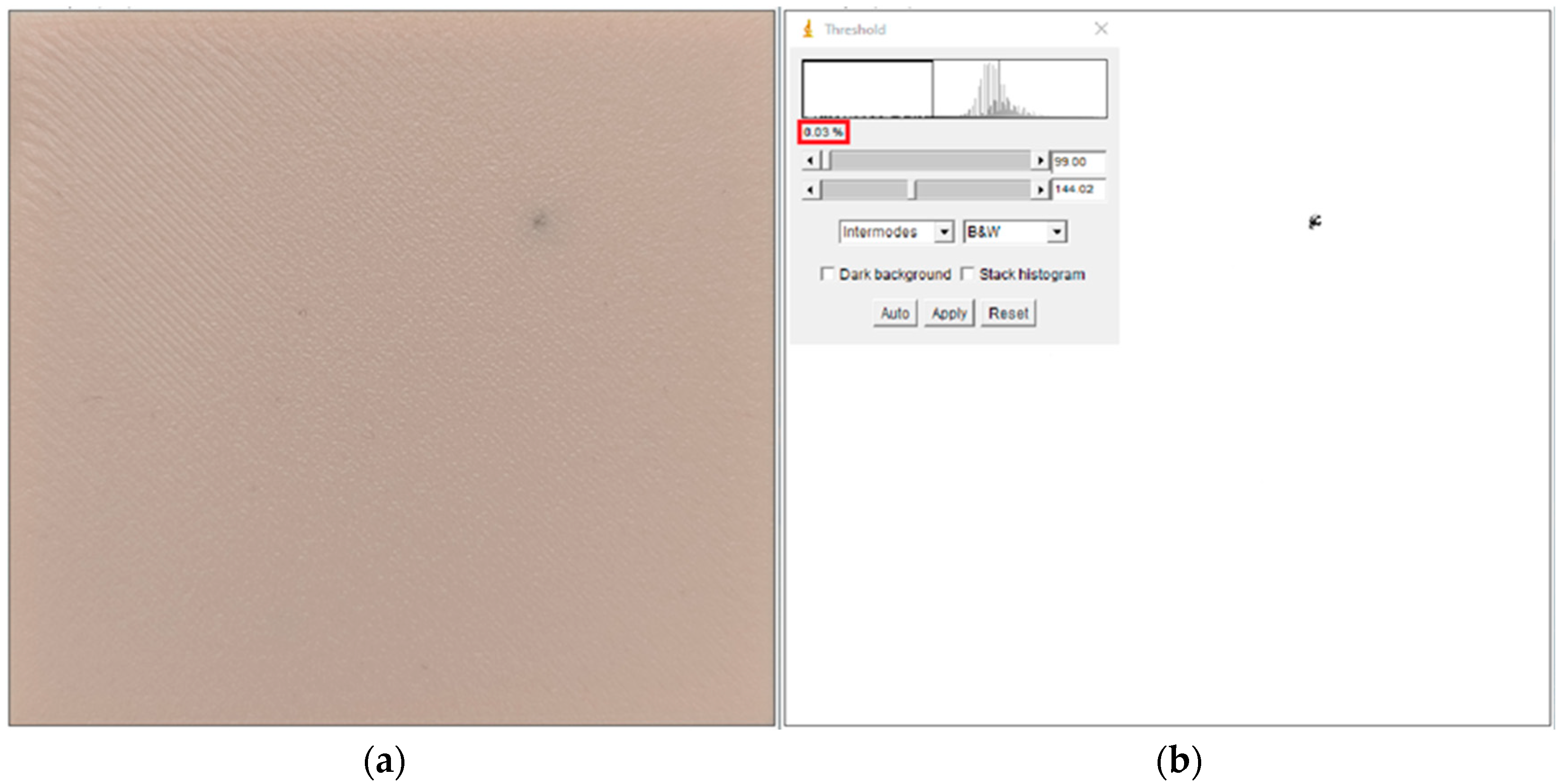
4.2. Image Processing Analysis

In this section, the structural damages of the samples that were punctured when the voltage was applied to their surfaces were evaluated. The image analysis method was used to evaluate the extent of these damages. For this purpose, sample surfaces were photographed at a 90° angle and a distance of 20 cm. The images obtained were analyzed with Image J software. In the analyses, the ratio of the area of structural damage caused by partial discharge and puncture events to the entire sample surface area was examined.
The samples received damages of different sizes according to the type of material they were produced from. As the voltage increased, the polymer material carbonized and burned due to the breakdown event that occurred as a result of partial discharges. Figure 9 shows the image analysis of the ABS material after breakdown. Image analysis results of ASA in Figure 10, PC/ABS in Figure 11, PETG in Figure 12, and PLA in Figure 13 are shared.
In Figure 9, it is seen that the ABS material is damaged superficially by 3.48% as a result of the breakdown. The damage pattern shows that the arcs occurring between the layers are intense.
In Figure 10, it is seen that the ASA material is damaged superficially by 1.39% as a result of the breakdown. The damage pattern shows that the arcs that occur between the layers progress without disintegration.
In Figure 11, it is seen that the PC/ABS material is damaged superficially by 3.49% as a result of the breakdown. The damage pattern shows that the arcs occurring between the layers are distributed in a limited way and progress by dispersion.
In Figure 12, it is seen that the PETG material is damaged superficially by 0.72% as a result of the breakdown. The damage pattern shows that the arcs occurring between the layers follow a layer path and progress without dispersion. In this context, the breakdown event occurred on the material carbonized by the electric arcs.
In Figure 13, it is seen that the PLA material is damaged superficially by 0.03% as a result of the puncture. The damage pattern shows that the arcs that occur between the layers propagate without breaking up. In this context, it is revealed that the electric arcs directly breakdown the PLA material.

4.3. Simulation Results of Electric Field Distribution Analysis

In this section, the electric field distribution analysis was performed with FEMM software, which adopts the finite element calculation method and is frequently used in studies of high voltage. The electric field distribution analysis was performed based on the electrode arrangement used in the experimental studies. Characteristic breakdown strength was applied to create the electric field. As a result of the simulation study, the image of the electric field exposed to the insulation material between the electrodes is shared in Figure 14.
Figure 14 shows the electric field distribution for the ABS material. Since the relative permittivity values are close to each other, the electric field distribution analysis results of other insulation materials are not shared. Figure 15 presents the graph created from the data obtained from the electric field distribution analysis.
The electric field density reaches its highest value at the boundary points where the corners of the electrodes begin to round. When the failed specimens are examined, the breakdown points and the possible breakdown points obtained in the simulation study match with each other.
The critical findings obtained from the study are presented in Table 5.

5. Conclusions

This study analyzed the behavior of solid insulation materials suitable for 3D printing when subjected to high voltage within the framework of insulation coordination. In this context, materials such as PLA, ABS, ASA, PETG, and PC/ABS, which are currently used or have potential as electrical insulators, were selected. The breakdown strength of the solid insulating materials produced via 3D printing were measured in the high-voltage laboratory in accordance with IEC-60243 standards. The Weibull distribution of the results obtained from the breakdown strength tests was assessed. Additionally, a detailed damage analysis of the breakdowns in the test specimens was conducted using ImageJ software.
The interpretation of the information obtained as a result of the study will determine the level of contribution to the literature. In this context, when looking at the data in Table 5, it is possible to say that the superficial damage ratio exhibits a similar behavior as the breakdown strength. As the high voltage applied to the material increases during experimental studies, the effect created by the electric arcs bridging between the layers of the material naturally increases. This shows that the breakdown strength of the material is high. In addition, it also reveals the effect of layered production on the breakdown strength, which occurs with 3D printing. The damage rate in the PLA material was 0.03%. Thus, the maximum breakdown strength of the material was measured as 24.82 kV/mm. The maximum breakdown strength of the PETG material was measured as 28.73 kV/mm, and the surface damage rate on the material was determined as 0.72%. Thus, the relationship between the damage rate and breakdown strength was determined. Another result obtained from the study is that the ASA material presents an exceptional situation. The breakdown strength and surface damage rate are outside the behavior of other materials.
As a result of the Weibull statistical distribution analysis, the voltage value at which the solid insulation material will be punctured with 95% probability was obtained. In the simulation study, the value of the maximum electric field intensity caused by the electric field irregularity occurring at the electrode edges was determined. When these two values are compared, the similarity of the experimental studies and the simulation study can be compared. While it is predicted that the ABS material will be punctured with 95% probability at 34 kV/mm, it is seen that it is exposed to a maximum electric field intensity of 33.74 kV/mm in the simulation study. The difference between the two values is calculated as 0.75%. While it is predicted that the PC/ABS material will be punctured with 32 kV/mm, it is determined that it is exposed to a maximum electric field of 33.04 kV/mm. The difference between these two values is calculated as approximately 3.25%. In this context, the effective role of the simulation study is revealed when evaluating the breakdown strength of solid insulation materials.
As seen in the image processing analysis studies carried out in Section 4.2, during the puncture, the electric current moved in the direction of the printing of the filaments. Due to the temperature changes that occur during printing, the shrinkage of the filament and the separation of the layers occur at the junction. Thus, the breakdown strength performance of the solid insulating material is directly affected. As a result of the studies, it was determined that the ASA material exhibited a different behavior than other materials between the damage ratio and breakdown strength because of this.
Another finding of this study is that three-dimensional printing technology holds potential for the production of high-voltage electrical equipment. Measurement results further revealed that high-voltage equipment can be successfully produced using three-dimensional printing technology, highlighting its potential as an innovative and cost-effective solution for manufacturing electrical components.

Funding

This research received no external funding, and the APC was funded by C.C.U.

Institutional Review Board Statement

Not applicable.

Informed Consent Statement

Not applicable.

Data Availability Statement

The original contributions presented in this study are included in the article/ Further inquiries can be directed to the corresponding author(s).

Conflicts of Interest

The authors declare no conflicts of interest.

References

  1. Kim, B.G.; Choi, H.H.; Park, H.Y.; Kwon, M.S.; Byeun, Y.K.; Kang, S.; Jung, Y.G.; Son, J.H.; Yang, S.C. Preparation and characterization of organic–inorganic hybrid coatings for improving the insulation properties of electrical steel. J. Coat. Technol. Res. 2023, 20, 1383–1393. [Google Scholar] [CrossRef]
  2. Zou, H.; Yin, Y.; Chen, J.; Zhang, S.; Tian, F. Research on the Inner Surface Discharge of the Insulation Sheath of Electric Locomotive Cable Terminals. Appl. Sci. 2024, 14, 9681. [Google Scholar] [CrossRef]
  3. Kadim, E.J.; Noorden, Z.A.; Adzis, Z.; Azis, N. Nanoparticles Application in High Voltage Insulation Systems. IEEE Trans. Dielectr. Electr. Insul. 2021, 28, 1380–1399. [Google Scholar] [CrossRef]
  4. Chapman, M.; Frost, N.; Bruetsch, R. Insulation systems for rotating low-voltage machines. In Proceedings of the Conference Record of the 2008 IEEE International Symposium on Electrical Insulation, Vancouver, BC, Canada, 9–12 June 2008; pp. 257–260. [Google Scholar] [CrossRef]
  5. Zhong, L.; Du, J.; Xi, Y.; Wang, F.; Wu, L.; Li, J.; Tu, M.; Li, X.; Fei, G. Multi-material and parameter-controllable stereolithography 3D printing of graded permittivity composites for high voltage insulators. Virtual Phys. Prototyp. 2023, 18, e2271447. [Google Scholar] [CrossRef]
  6. Bianchi, R.A.C.; Ferraz, H.F.; Gonçalves, R.S.; Moura, B.; Sudbrack, D.E.T.; Merini, A.; Machado, M.d.L.G.; Pires, R.; Homma, R.Z. A synthetic high-voltage power line insulator images dataset. Data Br. 2024, 55, 110688. [Google Scholar] [CrossRef]
  7. Li, Z.; Hsieh, E.; Li, Q.; Lee, F.C. High-Frequency Transformer Design with Medium-Voltage Insulation for Resonant Converter in Solid-State Transformer. IEEE Trans. Power Electron. 2023, 38, 9917–9932. [Google Scholar] [CrossRef]
  8. Guo, Y.; Tian, F.; Liu, H.; Yin, Y. Research on Ultra-Fast Transient Overvoltage Characteristics of Electric Locomotive. Appl. Sci. 2024, 14, 9561. [Google Scholar] [CrossRef]
  9. Divakaran, N.; Alex, Y.; Mohapatra, A.; Mohanty, S. Material extrusion-based 3D printed capacitor optimization: Enhancing performance with ZnO and Cu-CNT reinforced ABS composites. Appl. Mater. Today 2024, 40, 102363. [Google Scholar] [CrossRef]
  10. Cheng, F. Comparative study on the application of 3D printing and digital printing technology in fashion design. In Proceedings of the 2022 World Automation Congress (WAC), San Antonio, TX, USA, 11–15 October 2022; pp. 202–206. [Google Scholar] [CrossRef]
  11. Jaksic, N.I.; Desai, P.D. Characterization of 3D-printed capacitors created by fused filament fabrication using electrically-conductive filament. Procedia Manuf. 2019, 38, 33–41. [Google Scholar] [CrossRef]
  12. Zhou, Y. Research on development and problems of 3D printing technology under intelligent background. In Proceedings of the 2019 12th International Conference on Intelligent Computation Technology and Automation (ICICTA), Xiangtan, China, 26–27 October 2019; pp. 682–685. [Google Scholar] [CrossRef]
  13. Zhang, J.; Ding, B. Intelligent 3D Printing Technology in Architectural Design. In Proceedings of the 2023 3rd International Conference on Mobile Networks and Wireless Communications (ICMNWC), Tumkur, India, 4–5 December 2023; pp. 1–6. [Google Scholar] [CrossRef]
  14. Umair, M.; Kim, W.S. An Online 3D Printing Portal for General and Medical Fields. In Proceedings of the 2015 International Conference on Computational Intelligence and Communication Networks (CICN), Jabalpur, India, 12–14 December 2015; pp. 278–282. [Google Scholar] [CrossRef]
  15. Shi, Y. Research on the Combination of 3D Printing Technology and Computer Aided Industrial Design. In Proceedings of the 2022 4th International Conference on Smart Systems and Inventive Technology (ICSSIT), Tirunelveli, India, 20–22 January 2022; pp. 1231–1234. [Google Scholar] [CrossRef]
  16. Sahin, G.; Özyildirim, H.; Sahin, A. Investigation of mechanical and printing properties of poly(lactic acid) and its composite filaments used in 3D printing. Iran. Polym. J. 2024, 33, 79–91. [Google Scholar] [CrossRef]
  17. Li, S.; Izquierdo, B.S.; Gao, S. Analysis of 3D Printed Dielectric Resonator Antenna Arrays for Millimeter-Wave 5G Applications. Appl. Sci. 2024, 14, 9886. [Google Scholar] [CrossRef]
  18. Hua, L.; Bowen, P. Application of Ceramic 3D Printing Technology in Modern Ceramic Manufacturing. In Proceedings of the 2021 7th International Symposium on Mechatronics and Industrial Informatics (ISMII), Zhuhai, China, 22–24 January 2021; pp. 160–163. [Google Scholar] [CrossRef]
  19. Chankuson, P.; Chumsri, P.; Plodkaew, A. The Simulation of Dielectric Barrier Discharge for Breakdown Voltage in Starch Modification. Appl. Sci. 2023, 13, 12143. [Google Scholar] [CrossRef]
  20. Touzin, M.; Goeuriot, D.; Guerret-Piécourt, C.; Juvé, D.; Fitting, H.J. Alumina based ceramics for high-voltage insulation. J. Eur. Ceram. Soc. 2010, 30, 805–817. [Google Scholar] [CrossRef]
  21. Khalid, M.; Riaz, S.; Grekov, A.E.; Santi, E.; Naseem, S. High Breakdown Voltage Characteristics in Normally-Off 4H-SiC VJFET Using TCAD Simulation; Elsevier Ltd.: Amsterdam, The Netherlands, 2015; Volume 2. [Google Scholar]
  22. Zhang, T.; Du, J.; Lei, Y.; Cheng, Y.; Liu, W.; Yi, X.; Yin, J.; Yu, P. Effect of pores on dielectric breakdown strength of alumina ceramics via surface and volume effects. J. Eur. Ceram. Soc. 2020, 40, 3019–3026. [Google Scholar] [CrossRef]
  23. Balmelli, M.; Merotto, L.; Soltic, P.; Biela, J. Ignition detection with the breakdown voltage measurement during nanosecond repetitively pulsed discharges. Energy Convers. Manag. 2023, 292, 117382. [Google Scholar] [CrossRef]
  24. Akin, F.; Arikan, O.; Uydur, C.C. Analysis of Solid Insulating Materials Breakdown Voltages Under Different Voltage Types. Turk. J. Electr. Power Energy Syst. 2022, 2, 85–93. [Google Scholar] [CrossRef]
  25. Chen, G.; Zhao, J. Space charge and thickness dependent dc electrical breakdown of solid dielectrics. In Proceedings of the 2012 International Conference on High Voltage Engineering and Application, Shanghai, China, 17–20 September 2012; pp. 12–15. [Google Scholar] [CrossRef]
  26. BS EN 60243-1:2013; Electric Strength of Insulating Materials—Test Methods Part 1: Tests at Power Frequencies. BSI Standards Publication: London, UK, 2014; ISBN 978 0 580 83184 3.
  27. IEC 60060-1:2010; High-Voltage Test Techniques—Part 1: General Definitions and Test Requirements. International Electrotechnical Commission: Geneva, Switzerland, 2010.
  28. Akın, F. Katı Yalıtkan Malzemelerin Farklı Çalışma Koşulları Altında Performans Analizi. Master’s Thesis, Yıldız Technical University, İstanbul, Turkey, 2021. [Google Scholar]
  29. Awcock, G.J.; Thomas, R. Pattern Classification BT—Applied Image Processing; Awcock, G.J., Thomas, R., Eds.; Macmillan Education: London, UK, 1995; pp. 176–203. ISBN 978-1-349-13049-8. [Google Scholar]
  30. Huang, T.S.; Schreiber, W.F.; Tretiak, O.J. Image Processing. Proc. IEEE 1971, 59, 1586–1609. [Google Scholar] [CrossRef]
  31. Igathinathane, C.; Pordesimo, L.O.; Columbus, E.P.; Batchelor, W.D.; Methuku, S.R. Shape identification and particles size distribution from basic shape parameters using ImageJ. Comput. Electron. Agric. 2008, 63, 168–182. [Google Scholar] [CrossRef]
  32. Schindelin, J.; Rueden, C.T.; Hiner, M.C.; Eliceiri, K.W. The ImageJ ecosystem: An open platform for biomedical image analysis. Mol. Reprod. Dev. 2015, 82, 518–529. [Google Scholar] [CrossRef] [PubMed]
  33. Papadopulos, F.; Spinelli, M.; Valente, S.; Foroni, L.; Orrico, C.; Alviano, F.; Pasquinelli, G. Common tasks in microscopic and ultrastructural image analysis using ImageJ. Ultrastruct. Pathol. 2007, 31, 401–407. [Google Scholar] [CrossRef] [PubMed]
  34. Sahin, A. 3B Yazıcılarda Kullanılan Filamentler; All Sciences Academy: Konya, Türkiye, 2024; ISBN 978-625-6314-64-1. [Google Scholar]
  35. Qidi Tech. Available online: https://qidi3d.com/products/q1-pro-3d-printer (accessed on 1 November 2024).
  36. BS EN 60243-2:2014; Electric Strength of Insulating Materials—Test Methods Part 2: Additional Requirements for Tests Using Direct Voltage. BSI Standards Publication: London, UK, 2014; ISBN 978 0 580 83184 3.
  37. BS EN 60243-3:2014; Electric Strength of Insulating Materials—Test Methods Part 3: Additional Requirements for 1,2/50 μs Impulse Tests. BSI Standards Publication: London, UK, 2014; ISBN 978 0 580 83184 3.
  38. IEC 60060-2:2010; High-Voltage Test Techniques—Part 2: Measuring Systems. International Electrotechnical Commission: Geneva, Switzerland, 2010.
  39. Akin, F.; Arikan, O. Analysis of breakdown mechanism based on contact area and field enhancement factor of different electrode-material combinations. Int. J. Energy Res. 2022, 46, 12674–12686. [Google Scholar] [CrossRef]
  40. Akin, F.; Arikan, O. The effect of thermal aging on solid insulating materials: A case study for dielectric loss and dissipation factor based evaluations under different voltage levels and frequencies. Eng. Fail. Anal. 2023, 148, 107222. [Google Scholar] [CrossRef]
  41. Camalov, M.; Orucov, A.; Hashimov, A.; Arikan, O.; Akin, F. Breakdown strength analysis of XLPE insulation types: A comparative study for multi-layer structure and voltage rise rate. Electr. Power Syst. Res. 2023, 223, 109703. [Google Scholar] [CrossRef]
  42. White, J.S. The Moments of Log-Weibull Order Statistics. Technometrics 1969, 11, 373–386. [Google Scholar] [CrossRef]
Figure 1. Qidi Tech Q1 Pro 3D printer.
Applsci 14 11860 g001
Figure 2. Experimental container: (a) electrode configuration; (b) electrode arrangement.
Applsci 14 11860 g002
Figure 3. Connection diagram for breakdown strength tests.
Applsci 14 11860 g003
Figure 4. Cylindrical solid insulation test specimens. PETG, PC/ABS, PLA, ABS, and ASA from left to right.
Applsci 14 11860 g004
Figure 5. Square solid insulation test specimens. PETG, PC/ABS, ASA, ABS, and PLA from left to right.
Applsci 14 11860 g005
Figure 6. Box plot of breakdown strengths for cylindrical specimens.
Applsci 14 11860 g006
Figure 7. Box plot of breakdown strengths for square specimens.
Applsci 14 11860 g007
Figure 8. Weibull distribution of breakdown strengths for materials.
Applsci 14 11860 g008
Figure 9. Results of image analysis for ABS: (a) breakdown sample; (b) analysis of image.
Applsci 14 11860 g009
Figure 10. Results of image analysis for ASA: (a) breakdown sample; (b) analysis of image.
Applsci 14 11860 g010
Figure 11. Results of image analysis for PC/ABS: (a) breakdown sample; (b) analysis of image.
Applsci 14 11860 g011
Figure 12. Results of image analysis for PETG: (a) breakdown sample; (b) analysis of image.
Applsci 14 11860 g012
Figure 13. Results of image analysis for PLA: (a) breakdown sample; (b) analysis of image.
Applsci 14 11860 g013
Figure 14. Results of simulation for electric field distribution.
Applsci 14 11860 g014
Figure 15. Results of electric field distribution for test specimens.
Applsci 14 11860 g015
Table 1. Physical, mechanical, thermal, and electrical properties of the filaments [34].
ParametersABSASAPC/ABSPETGPLA
Density (g/m3)1.031.061.131.281.23
Melt Flow Index (g/10min)5.222122017.3
Tensile Strength (MPa)4448605356
Elastic Modulus (MPa)21002100220030002850
Elongation at Break (%)401275307
Notched Impulse Test (kJ/m2)38171314.214.2
Heat Bending Temperature (°C)95951208055
Glass Transition Temperature (°C)95–105100–105125–13580–8555–60
Surface Resistance (Ω/sq)>1012>1012>1012>1012>1012
Relative Permittivity33.32.933.1
Table 2. Qidi Tech Q1 Pro 3D printer technical specifications [35].
ParameterQidi Tech Q1 Pro 3D
Print Size (W×D×H)245 × 245 × 240 mm
XY StructureCoreXY
Print Head Temperature≤350 °C
Hot Bed Temperature≤120 °C
Max Speed of Tool Head600 mm/s
Chamber Temperature60 °C Independent Chamber Heating
Recommended FilamentPLA, ABS, ASA, PETG
Compatible FilamentTPU, PA, PC, Carbon/Glass Fiber-Reinforced Polymer
Automatic LevelingHands-free Automatic Leveling
Table 3. Parameters of 3D printing by the filament type.
ParametersABSASAPC/ABSPETGPLA
Nozzle diameter (mm)0.40.40.40.40.4
Layer height (mm)0.20.20.20.20.2
Sparse infill density (%)100100100100100
Sparse infill patternRectilinearRectilinearRectilinearRectilinearRectilinear
Nozzle temperature (°C)283275283240220
Build plate (°C)1101001108060
Chamber temperature (°C)535353--
Initial layer print speed (mm/s)5050505050
Initial layer infill print speed (mm/s)105105105105105
Outer wall print speed (mm/s)200200200200200
Inner wall print speed (mm/s)300300300300300
Print cooling enableNoYesNoYesYes
Table 4. Qidi Tech Q1 Pro 3D printer technical specifications.
Weibull ParameterPLAABSASAPETGPC/ABS
α23.9231.3621.0527.9230.78
β27.3513.6814.8342.2725.70
Table 5. Outcomes from the study.
ParameterPLAABSASAPETGPC/ABS
Breakdown Strength
(max) [kV/mm]
24.8234.3322.7328.7332.09
Breakdown Strength
(critical) [kV/mm]
23.9231.3621.0027.9230.78
Breakdown Strength
(%95) [kV/mm]
2434222832
Electric Field
(max) [kV/mm]
25.7933.7422.8030.0433.04
Damage Ratio0.03%3.48%1.39%0.72%3.49%
Disclaimer/Publisher’s Note: The statements, opinions and data contained in all publications are solely those of the individual author(s) and contributor(s) and not of MDPI and/or the editor(s). MDPI and/or the editor(s) disclaim responsibility for any injury to people or property resulting from any ideas, methods, instructions or products referred to in the content.

