Abstract
Integrated circuits suffer severe deterioration due to single-event upsets (SEUs) in irradiated environments. Spin-transfer torque magnetic random-access memory (STT-MRAM) appears to be a promising candidate for next-generation memory as it shows promising properties, such as non-volatility, speed, and unlimited endurance. One of the important merits of STT-MRAM is its radiation hardness, thanks to its core component, a magnetic tunnel junction (MTJ), being capable of good function in an irradiated environment. This property makes MRAM attractive for space and nuclear technology applications. In this paper, a novel radiation-hardened triple modular redundancy (TMR) design for anti-radiation reinforcement is proposed based on the utilization of STT-MTJ devices. Simulation results demonstrate the radiation-hardened performance of the design. This shows improvements in the design’s robustness against ionizing radiation.
1. Introduction
Radiation effects on semiconductor electronic devices have been one of the main concerns of the microelectronic industry, not only for space applications, but also for consumer electronics [1,2,3,4]. Regarding the reliability of electronic products, radiation causes critical damage which threatens the normal operation of integrated circuits based on complementary metal-oxide semiconductor (CMOS) technology. With the shrinking of CMOS fabrication nodes, critical charge and transistor threshold voltages are reduced, and radiation effects become more critical even at a very low level. To describe radiation effects, two types of models are generally used, namely total ionizing dose (TID) and single-event effects (SEEs) as a result of particles colliding with electronic devices [5,6].
When particles and high-energy rays are injected into semiconductor materials, electron/hole pairs are created after the interaction. The electrons and holes induced by radiation are further recombined, transported, or trapped under electric fields. When the radiant energy accumulates to a certain value, it will damage the electrical performance of CMOS transistors and even lead to permanent failure. The impact of TID on CMOS-based circuits is mainly manifested in two aspects. On one hand, the threshold voltage of the CMOS transistor shifts, which will change the opening degree of the CMOS transistor and cause a shift in the corresponding circuit parameters; on the other hand, it causes an increase in the leakage current, resulting in an increase in circuit power consumption and a shift in the operating point. Both of these aspects may greatly reduce the performance of the CMOS system and even result in complete failure. Due to scaling of CMOS technology, the effects of TID on gate threshold voltage can be negligible in CMOS technologies when the gate oxide thickness is less than 4 nm.
When radiation particles with high energy pass through the sensitive area of a CMOS device, the material will ionize electron/hole pairs, and these charges will be transported and collected, resulting in a transient current, which may change the working state of the circuit and even cause irreversible damage to the device. With the rapid scaling down of CMOS technology, SEEs have recently become a substantial threat for the reliability of advanced CMOS technologies, as they result in integrated circuit logic function errors. In fact, single-event upsets (SEUs) have become the largest contributor to CMOS system soft error rates as the amount of charge, which represents stored information, has dropped lower and lower. SEUs mainly occur in memory devices and logic circuits, which may cause “soft” errors in flip-flops, memory cells, and digital circuits. SEUs are therefore a significant concern not only for electronics operating in outer space, but also for digital systems that must work reliably.
One emerging nonvolatile memory technology, spin-transfer torque magnetic random-access memory (STT-MRAM), becomes an ideal candidate for next-generation memory given its characteristics of non-volatility, high writing speed, and near-infinite endurance. Currently, perpendicular-anisotropy magnetic tunnel junctions (MTJs) are preferred for STT-MRAM due to their adequate storage retention and good scalability. In addition, the storage element of STT-MRAM has been experimentally proved to be highly tolerant to radiation effects [4,7,8,9]. Since it utilizes the electron spin degree of freedom to store digital data instead of electron charges, the nanoscale MTJ is considered to be radiation-hardened, which makes it attractive for applications in space technology. Fanghui Ren et al. [10] demonstrated that the electrical and the magnetic properties of MgO-based MTJs were not affected by gamma radiation and epithermal neutrons. Eric Arturo Montoya et al. [11] proved that the critical properties of nanoscale perpendicular magnetic anisotropy in STT-MTJs, such as magnetoresistance, magnetic field switching, and current-induced switching, are robust against ionizing radiation.
The triple modular redundancy (TMR) method is commonly used for better reliability in digital integrated circuits, especially large-scale memory and programmable logic arrays. However, the TMR module itself suffers the potential danger of SEE, which also decreases circuit reliability. Methods of making TMR modules extremely radiation-hardened have rarely been discussed in the literature before; therefore, it is worth considering whether TMR can be strengthened by utilizing the inherent anti-radiation characteristics of MTJ devices. In this paper, a novel triple modular redundancy (TMR) anti-radiation reinforcement design based on STT-MTJ devices is proposed. With STT-MTJ devices contributing to the majority voter circuits, the TMR module itself can be considered truly radiation-hardened. Furthermore, the proposed design was numerically analyzed to verify its functional behavior through simulation. The simulation results demonstrate improvements to the digital system’s robustness against ionizing radiation.
This paper is organized as follows: in Section 2, the method of using STT-MTJ devices to reduce radiation damage is described with an emphasis on and sufficient details regarding STT-MTJ mechanisms. Then, the radiation-hardening solution of introducing the STT-MTJ devices into the optimized TMR circuits is discussed in Section 3. Afterwards, its enhanced robustness is demonstrated with simulation results in Section 4. Finally, conclusions are drawn in Section 5.
2. Materials and Methods
TMR is widely used for reducing device failure, as it rapidly detects and corrects SEUs [12,13,14,15,16]. A diagram of a traditional TMR is shown in Figure 1. It consists of four majority voters and multiple data paths. Each data path has an independent input to avoid voting errors due to the propagation of the previous error inputs. Under normal working conditions, the three modules offer three identical outputs at the same time. The core principle of TMR is an operation called majority voting on the output of the three data paths. Thus, in a traditional TMR circuit, each majority voter is critical because it is required to tolerate the errors caused by unexpected radiation. If there is an SEU error in one of the three channels of data, the system will determine the correct output through the majority voting operation to achieve SEU error correction. Therefore, a majority voting circuit based on STT-MTJ is proposed here to improve robustness against radiation.
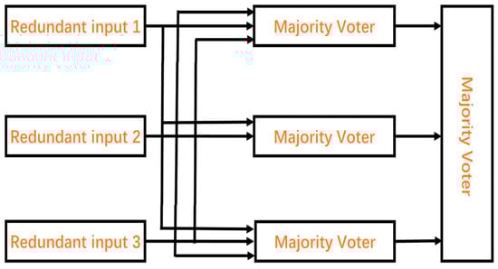
Figure 1.
Traditional TMR system with four majority voters.
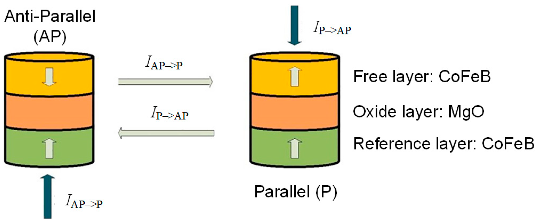
To increase the robustness of the TMR module itself, MTJ devices were used in a TMR system for the first time. A perpendicular-anisotropy MTJ is preferred for use in STT-MTJ due to its adequate storage retention and good scalability. The MTJ is a three-layered stack which is composed of two ferromagnetic (FM) layers and a thin MgO barrier layer in between them. Its schematic structure is shown in Figure 2. Due to the effect of giant magnetoresistance (GMR), the resistance of the MTJ is determined by the relative magnetic orientation of the two FM layers, namely the free layer and the reference layer. The parallel (P) state means that the two FM layers of the MTJ share the same magnetic direction, resulting in a low resistance to currents passing through the device, and is therefore represented by the binary data value “0”. In the figure, RP is used to denote the low resistance value. In contrast, the anti-parallel (AP) state indicates that the magnetic directions of the two FM layers are opposites, corresponding to a high resistance, and is represented by the binary data value “1”. The high resistance value is denoted by RAP in the figure. The value of the tunnel magnetoresistance ratio (TMRa) is used to characterize the resistance variation, as shown in Equation (1).
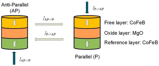
Figure 2.
Schematic of an STT-MTJ device corresponding to two states, namely the P and AP states.
The magnetic orientation of the free layer can be changed according to the STT mechanism. Specifically, the state of the STT-MTJ can be manipulated by injecting it with spin-polarized current. The STT-MTJ switches from the P to AP state when spin-polarized current IP- > AP flows through the STT-MTJ from the free layer to the reference layer, and from the AP to P state when spin-polarized current IAP- > P is injected in the opposite direction, as shown in Figure 2.
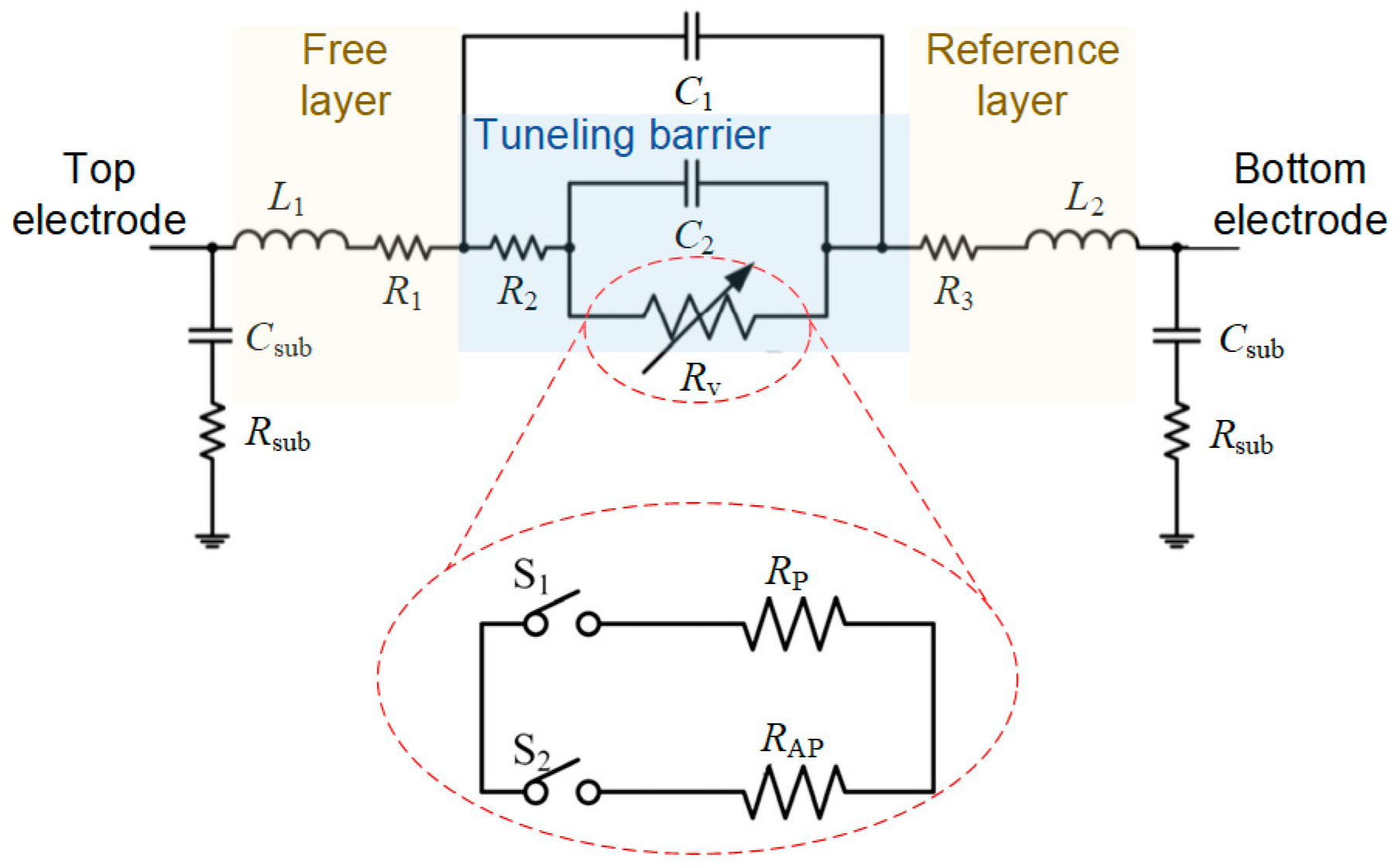
Based on the STT-MTJ mechanisms, an equivalent circuit for the MTJ device used for simulation purposes is illustrated in Figure 3. Given the fact that digital behaviors are high-frequency, RC networks derived from substrate coupling are necessarily attached to the input and output ports to improve simulation accuracy. In this model, R1 and R3 are the parasitic resistance of the top and bottom electrodes, respectively. R2 is the total parasitic resistance of both the metallic FM layers. C1 is the parasitic capacitance between the two FM layers across the peripheral oxide layer. C2 is the film capacitance of the core oxide layer, which acts a functional tunneling barrier. Similar to R1 and R3, L1 and L2 are the parasitic inductances induced by the top and bottom electrodes. The key trait of the GMR effect is dynamic resistance Rv, which is simulated with a switch circuit, as highlighted in the figure. When the MTJ functions in the P state, switch S1 turns on and S2 turns off. Vice versa, only S2 is on in the AP state.
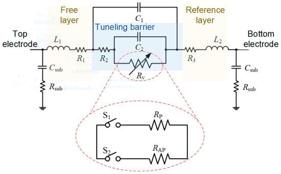
Figure 3.
Schematic of an equivalent circuit of the MTJ device used in simulation.
The parameters used in this model are referenced from [17] and listed in Table 1. Thus, this equivalent circuit for the MTJ device is ready to be embedded in the TMR module presented in the following section. The whole TMR circuit, including multiple CMOS transistors and MTJ devices, was simulated with the Synopsys HSpice software of version E-2010.12 at the 65 nm technology node.

Table 1.
The parameters used in the equivalent circuit model for the MTJ device simulation.
3. Results
As energetic particles strike the sensitive nodes of the transistors, the charge accumulated on the sensitive node reaches a critical state, which may cause soft errors, namely SEUs. Considering α-particles only in this paper, a double exponential current source is commonly used to simulate the process of α-particles hitting the sensitive nodes. To model the injection of a particle strike and its associated deposited charge, an injection model from [18] is adopted, which is widely used in relevant research [18,19,20,21,22]. This behavior of the particle hitting on the sensitive nodes of the CMOS device can be modeled as a double exponential current source, which can be expressed by Equation (2):
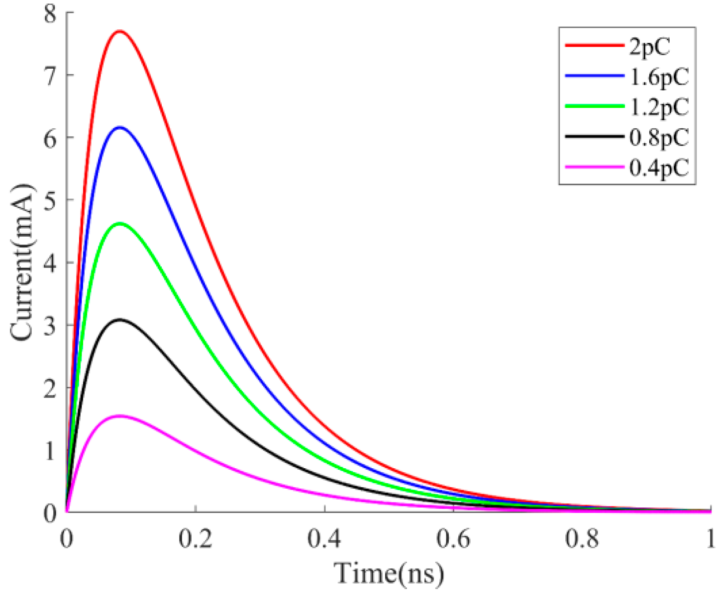
where Qinj is the charge injected into a CMOS device with a typical value from −2 to 2 pC (a positive value for NMOS and a negative value for PMOS), τ1 is the collection time constant with a typical value of 150 ps, and τ2 is the establishment time constant with a typical value of 50 ps. As radiation particles hit the sensitive nodes, different particle energy levels lead to diverse linear energy transfer (LET). Figure 4 shows the transient response of the double exponential current source with different values of Qinj. It is seen from the figure that a relatively low-charge pC level is able to induce a harmful leakage of current, of which the peak value reaches the mA level and the duration lasts for up to 0.4 ns. In addition, the peak value increases linearly with the injected charge. This transient response was used as the stimulation in the following simulations of the designed circuits.
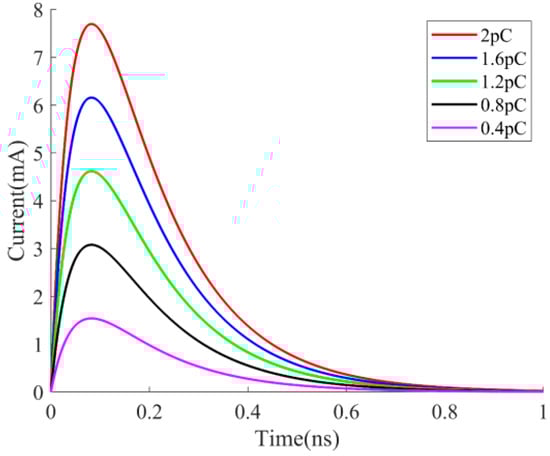
Figure 4.
The transient responses of the double exponential current pulses with various values of Qinj, including 2 pC, 1.6 pC, 1.2 pC, 0.8 pC, and 0.4 pC.
A spintronic TMR design based on STT-MTJ devices, which can be used to significantly decrease the impact of radiation, was developed to elevate the robustness of CMOS circuits. Focusing on maximizing the immunity to soft errors caused by SEUs, the proposed TMR circuits successfully optimized the traditional CMOS-based TMR circuits, as numerically shown in this section.
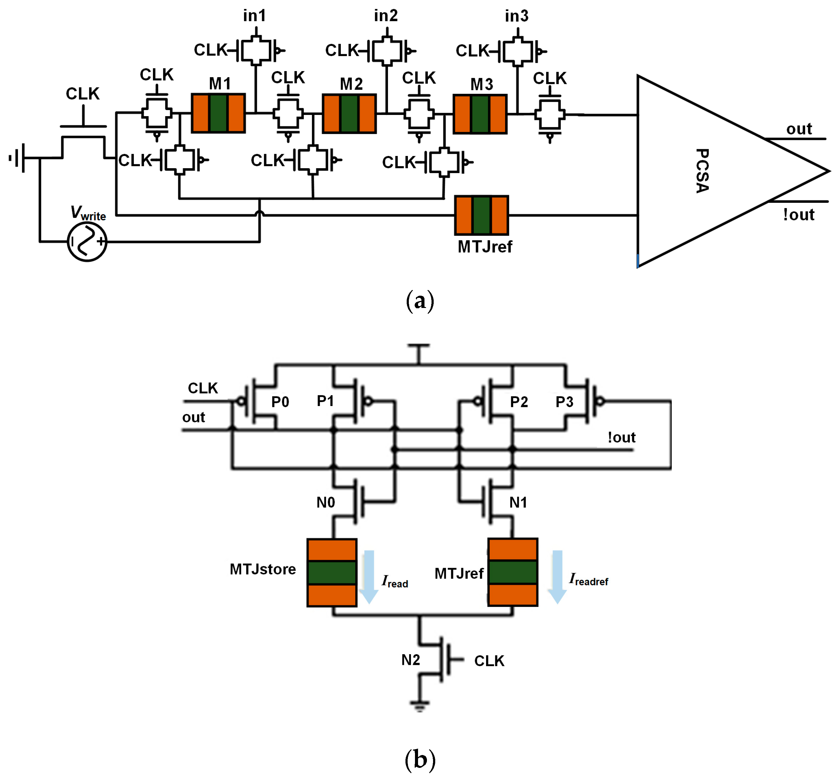
Figure 5 shows the schematic of the proposed TMR circuit based on STT-MTJ devices. It is an optimization technique to increase robustness against SEUs. The STT-MTJ devices show excellent anti-radiation properties. In Figure 5a, the MTJ device can be regarded as a register. First, the input is divided into three data paths. Then, the data are written into the STT-MTJ devices, in which the devices are connected in series by the peripheral circuit. Afterwards, a pre-charge sense amplifier (PCSA) circuit is used for the amplification of the output logic signal. Figure 5b shows the schematic of the PCSA used in the novel majority voter circuit. As shown in Figure 5a, the proposed circuit includes the STT-MTJ devices and the corresponding transmission gates (TGs). The operations of the circuit can be classified into two modes, namely the writing and reading modes.

Figure 5.
Schematic of (a) the designed TMR circuit based on STT-MTJ devices and (b) the PCSA circuit.
In writing mode, the writing operation occurs when the clock (CLK) signal is low. Therefore, the writing path includes the three inputs and the reference voltage source Vwrite, which is set to be 0.5Vdd in this study. The reading path and writing path are isolated from each other by the remaining transmission gates. The current direction is determined by the potential difference between the input and the reference voltage Vwrite. When this operation writes a data value of “0”, the current is larger than the critical switching current, flowing through the STT-MTJ device from the reference layer to the free layer. When writing a value of “1”, the current runs in exactly the opposite direction. In addition, the devices’ TG sizes are critical for the writing operations. A detailed design of the sizes of the TGs should consider several aspects, including the switching current and frequency of the MTJ device, as well as the power consumption. In this paper, the writing current is set to be 173 µA and the writing time is 2.6 ns.
In reading mode, the CLK signal is set to be high during the reading operation. The reading path includes the PCSA, four TGs, the reference MTJ (MTJref) device, and the three MTJs used for data storage (MTJstore). Different states of the MTJ devices correspond to different resistances, in which RP for logic “0” and RAP for logic “1”. The stored data can be sensed when the reading current passes through the MTJref device and the MTJstore devices, respectively. For the reading process, one of the key parameters that influences the error rate of the reading operation is the resistance of the MTJref device. In addition, the resistance of the TGs should also be taken into consideration during the reading operation. The resistance of the MTJref device can be expressed by the following equation:
where RTG is the resistance of the TG, and RP and RAP are the resistance of the MTJ devices in the P and AP states, respectively.
Furthermore, the reading speed is also influenced by the sizes of the transistors in the PCSA. With the key parameters such as speed and power satisfied, the minimum transistor sizes were adopted in the designed circuit to save on chip area and power. Assuming that the output is pre-charged, the reading speed is mainly determined by the high-level to low-level propagation delay. Theoretically, the fastest reading speed corresponds to a case where all the MTJs have the correct values. Based on the simulation results, the reading process can be completed within 130 ps. In cases where radiation-induced faults occur, the reading process could take up to 240 ps.
4. Discussion
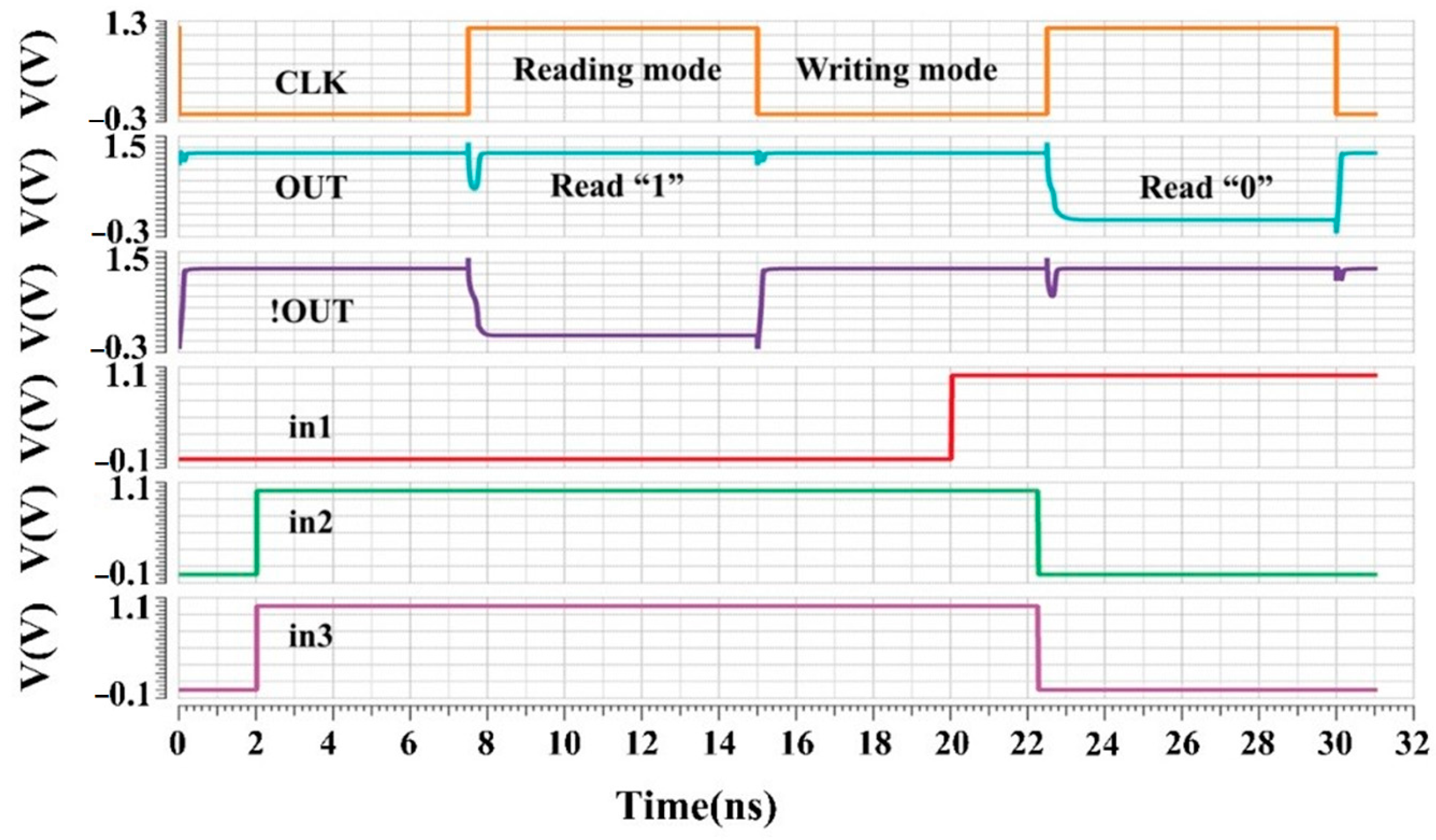
Figure 6 shows the transient simulation results of the proposed majority voter system. The three input channels, namely in1, in2, and in3, are three data paths which accept the same data from the front stage. It is assumed that the input channel in1 accidentally introduces an error and is used to represent an input signal which is affected by an SEU. At three time points, namely 2, 20, and 22.2 ns, the input channel in1 is not able to function normally. For example, it maintains a value of “0” when other voters change to “1” at the simulation time of 2 ns. As can be seen, the other two input channels share the same signal, representing the “majority”. So, the output should never be affected by the status of in1. Figure 6 shows that the simulation results are in accord with these analyses. At 2 ns with the CLK at a low level, it is in writing mode and the data should be successfully written into the STT-MTJ device. Therefore, the storage cell should be the same as in2 (or in3) and not be affected by in1. Then, in the following period of time in the reading mode from 7.5 to 15 ns, the output is validated to be “1”. Similarly, we can also find out that at 22.5 ns, “0” derived from the majority in2 and in3 is successfully written into the storage cell and is read out correctly thereafter. This simulation reveals that the output is not affected by the error from in1, and indicates that the designed majority voter based on STT-MTJ devices can realize the correct logic function of TMR.
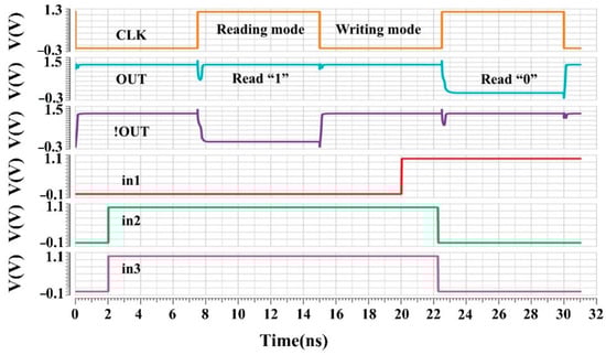
Figure 6.
Transient simulation results of the majority voter circuit based on STT-MTJ devices.
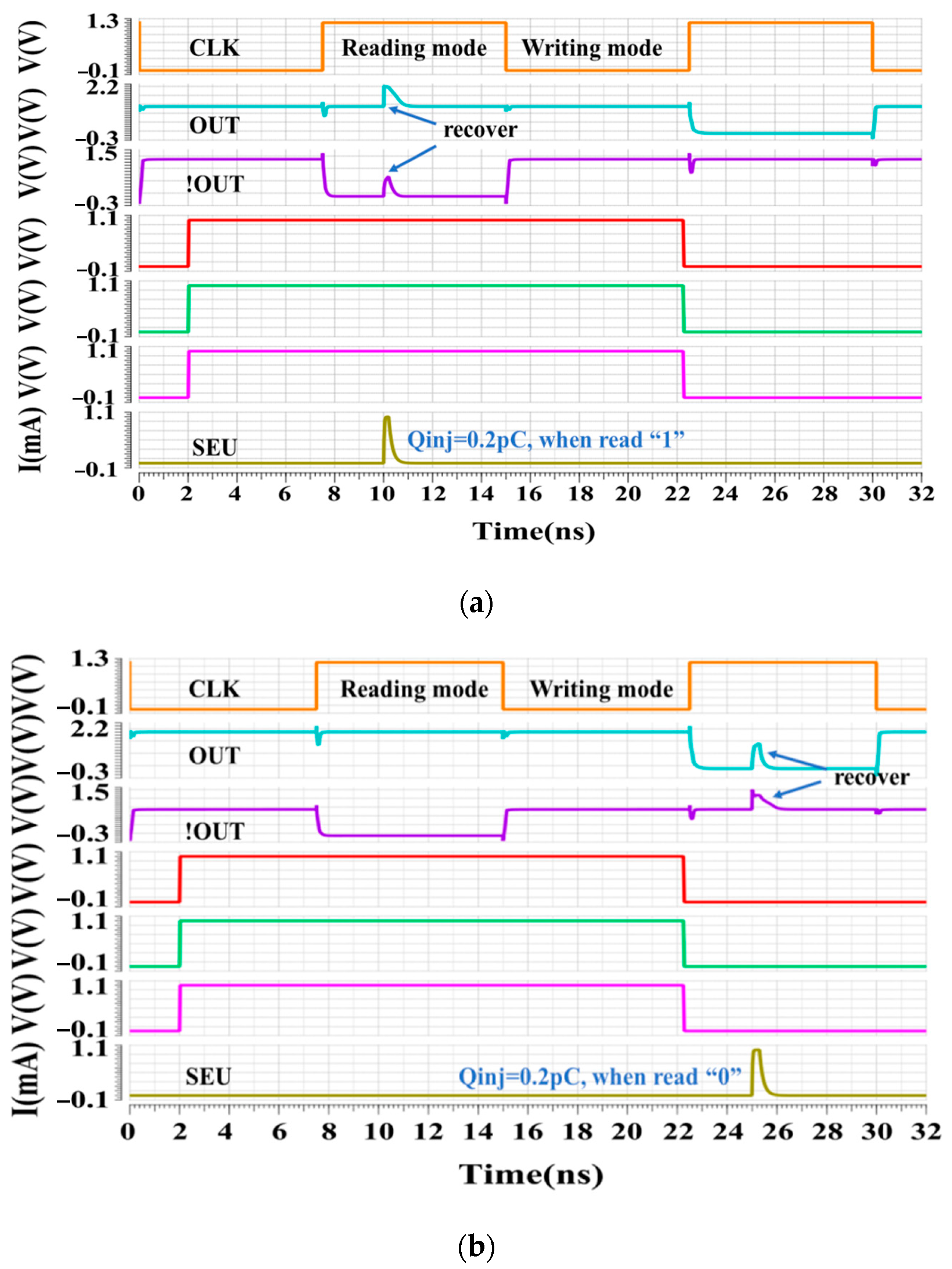
Furthermore, the simulation results show that the output can be recovered from the error state when the circuit encounters SEUs. Figure 7 demonstrates the anti-irradiation functionality of the proposed TMR module. According to the data stored in STT-MTJ devices, the sensitive nodes can be represented by Q or ~Q. Here, Q and ~Q are representing the storage of “1” and “0”, respectively. When high-energy particles hit the sensitive nodes under certain radiation levels, the deposited charges can be used to reduce the diverse LET. Since the amplitude of the LET is proportional to the particles’ energy, an injected charge Qinj of 0.2 pC is assumed. In Figure 7a, it is assumed that an SEU which occurred at 10 ns induced an injection of a 0.2 pC charge into the sensitive storage cell. At this time, a high voltage level represented by “1” is stored in the sensitive node, which can be verified by the fact that the CLK is low and the three input signals switch from “0” to “1” at 2 ns. Generally, the injection of negative charge has the ability to toggle the output. Interestingly, the simulation results show that the output only has a slight fluctuation. It is the TMR system that prevents the signal from toggling the wrong output and quickly recovers the correct output. This can be explained by the different charge storage pattern in MTJs. The charge stored in the MTJ devices of the majority voter circuit still has an impact on the sensitive node, while the traditional TMR output is separated from the storage cell by a TG and depends on a clock signal to refresh the sensitive node. Therefore, the MTJ device from the majority voter is able to drag the output back with the help of the PCSA circuit. As a result, the data stored in the sensitive node are recovered. The simulation results of reading “0” are shown in Figure 7b. The CLK is low at the time of 25 ns. It is similar to the operation of reading “1”. As the MTJ devices are still carrying “0”, the TMR system is able to prevent the signal from toggling and recovers it. All of the SEUs can only induce a small fluctuation in the outputs. The simulations prove that the output can be recovered successfully from an SEU in both operations. Therefore, the proposed TMR circuit shows a certain tolerance to SEUs.
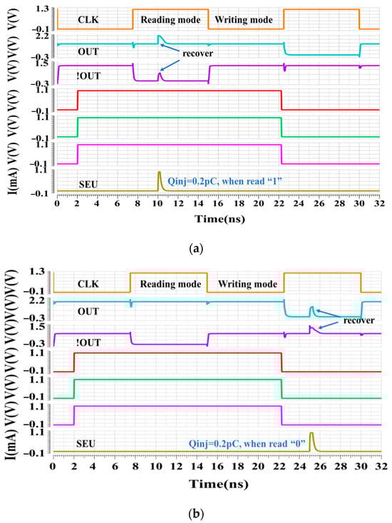
Figure 7.
Transient simulation waveforms of corrected output from the proposed TMR circuit when SEU occurs with Qinj = 0.2 pC (a) read “1” and (b) read “0”.
5. Conclusions
With the development of large-scale integrated circuits and semiconductor technology, the digital systems for critical data storage suffer from the damage of SEUs. In this paper, a novel radiation-hardened TMR circuit design based on STT-MTJ devices is proposed. Based on an equivalent circuit model for MTJ devices, the whole TMR module is simulated. The simulation results validate the anti-radiation reinforcement qualities of the proposed circuit. On the one hand, the STT-MTJ devices constitute a correct logic pattern of majority voters and achieved basic TMR functionality. On the other hand, the STT-MTJ devices contribute to a pre-charge sense amplifier with the ability to recover the storage cell. Improved anti-radiation properties and robustness of the TMR circuit against SEUs is achieved. The designed TMR circuit can be used in irradiated environments to control and reduce radiation-related operation failures. Further study can focus on the speed and power performance of this TMR circuit.
Author Contributions
Conceptualization, S.Z. and Y.C.; Data Curation, P.D. and N.L.; Formal Analysis, S.Z.; Funding Acquisition, S.Z.; Investigation, P.D.; Methodology, S.Z. and P.D.; Project Administration, Y.C.; Resources, S.Z.; Software, P.D. and N.L.; Supervision, Y.C.; Validation, S.Z.; Visualization, N.L.; Writing—Original Draft, P.D. and N.L.; Writing—Review and Editing, S.Z. All authors have read and agreed to the published version of the manuscript.
Funding
This research was funded by the National Natural Science Foundation of China, grant number 62204100; the China Postdoctoral Science Foundation, grant number 2021M691360; and the Postdoctoral Research Foundation of Zhejiang Province, grant number ZJ2020101.
Data Availability Statement
The original contributions presented in the study are included in the article, further inquiries can be directed to the corresponding author.
Acknowledgments
Special thanks for the technical support from IGEN Tech Co., Ltd.
Conflicts of Interest
The authors declare no conflict of interest.
References
- Gang, Y.; Zhao, W.S.; Klein, J.O.; Chappert, C.; Mazoyer, P. A High-Reliability, Low-Power Magnetic Full Adder. IEEE Trans. Magn. 2011, 47, 4611–4616. [Google Scholar] [CrossRef]
- Nikonov, D.E.; Bourianoff, G.I.; Ghani, T. Proposal of a Spin Torque Majority Gate Logic. IEEE Electron Device Lett. 2011, 32, 1128–1130. [Google Scholar] [CrossRef]
- Nikonov, D.E.; Young, I.A. Overview of Beyond-CMOS Devices and a Uniform Methodology for Their Benchmarking. Proc. IEEE 2013, 101, 2498–2533. [Google Scholar] [CrossRef]
- Wang, B.; Wang, Z.H.; Du, A.; Qiang, Y.; Cao, K.; Zhao, Y.F.; Zheng, H.C.; Yan, S.H.; Zhai, P.F.; Liu, J.; et al. Radiation impact of swift heavy ion beams on double-interface CoFeB/MgO magnetic tunnel junctions. Appl. Phys. Lett. 2020, 116, 172401. [Google Scholar] [CrossRef]
- Zimmermann, R.; Fichtner, W. Low-power logic styles: CMOS versus pass-transistor logic. IEEE J. Solid-State Circuits 1997, 32, 1079–1090. [Google Scholar] [CrossRef]
- Fazeli, M.; Miremadi, S.G.; Ejlali, A.; Patooghy, A. Low energy single event upset/single event transient-tolerant latch for deep subMicron technologies. IET Comput. Digit. Tech. 2009, 3, 289–303. [Google Scholar] [CrossRef]
- Kobayashi, D.; Kakehashi, Y.; Hirose, K.; Onoda, S.; Makino, T.; Ohshima, T.; Ikeda, S.; Yamanouchi, M.; Sato, H.; Enobio, E.C.; et al. Influence of Heavy Ion Irradiation on Perpendicular-Anisotropy CoFeB-MgO Magnetic Tunnel Junctions. IEEE Trans. Nucl. Sci. 2014, 61, 1710–1716. [Google Scholar] [CrossRef]
- Seifu, D.; Peng, Q.; Sze, K.; Hou, J.; Gao, F.; Lan, Y.C. Electromagnetic Radiation Effects on MgO-Based Magnetic Tunnel Junctions: A Review. Molecules 2023, 28, 4151. [Google Scholar] [CrossRef]
- Vilkov, E.A.; Chigarev, S.G.; Malikov, I.V.; Chernykh, A.V.; Maryshev, S.N. Electromagnetic Radiation under Spin Injection in a Tunnel Magnetic Junction with a NiO Spacer. J. Commun. Technol. Electron. 2021, 66, 459–464. [Google Scholar] [CrossRef]
- Ren, F.H.; Jander, A.; Dhagat, P.; Nordman, C. Radiation Tolerance of Magnetic Tunnel Junctions With MgO Tunnel Barriers. IEEE Trans. Nucl. Sci. 2012, 59, 3034–3038. [Google Scholar]
- Montoya, E.A.; Chen, J.R.; Ngelale, R.; Lee, H.K.; Tseng, H.W.; Wan, L.; Yang, E.; Braganca, P.; Boyraz, O.; Bagherzadeh, N.; et al. Immunity of nanoscale magnetic tunnel junctions with perpendicular magnetic anisotropy to ionizing radiation. Sci. Rep. 2020, 10, 10220. [Google Scholar] [CrossRef] [PubMed]
- Wang, Y.; Cai, H.; Naviner, L.A.D.; Zhang, Y.; Zhao, X.X.; Deng, E.; Klein, J.O.; Zhao, W.S. Compact Model of Dielectric Breakdown in Spin-Transfer Torque Magnetic Tunnel Junction. IEEE Trans. Electron Devices 2016, 63, 1762–1767. [Google Scholar] [CrossRef]
- Danilov, I.A.; Gorbunov, M.S.; Antonov, A.A. SET Tolerance of 65 nm CMOS Majority Voters: A Comparative Study. IEEE Trans. Nucl. Sci. 2014, 61, 1597–1602. [Google Scholar] [CrossRef]
- Kshirsagar, R.V.; Patrikar, R.M. Design of a novel fault-tolerant voter circuit for TMR implementation to improve reliability in digital circuits. Microelectron. Reliab. 2009, 49, 1573–1577. [Google Scholar] [CrossRef]
- Luo, Y.H.; Zhang, F.Q.; Wang, Y.P.; Wang, Y.M.; Guo, X.Q.; Guo, H.X. Single event upsets sensitivity of low energy proton in nanometer static random access memory. Acta Phys. Sin. 2016, 65, 068501. [Google Scholar]
- Bagatin, M.; Gerardin, S.; Paccagnella, A.; Visconti, A.; Virtanen, A.; Kettunen, H.; Costantino, A.; Ferlet-Cavrois, V.; Zadeh, A. Single Event Upsets Induced by Direct Ionization from Low-Energy Protons in Floating Gate Cells. IEEE Trans. Nucl. Sci. 2017, 64, 464–470. [Google Scholar] [CrossRef]
- Liu, X.; Xu, C.; Yu, P.P.; Jiang, Y.F. Calibration and Parameter Extraction of STT-MTJ Device at High Frequency by Using De-Embedding Approach Based on TRL Calibration. IEEE Trans. Electron Devices 2021, 68, 271–278. [Google Scholar] [CrossRef]
- Wang, Y.; Zhang, Y.; Deng, E.Y.; Klein, J.O.; Naviner, L.A.B.; Zhao, W.S. Compact model of magnetic tunnel junction with stochastic spin transfer torque switching for reliability analyses. Microelectron. Reliab. 2014, 54, 1774–1778. [Google Scholar] [CrossRef]
- Rajaei, R.; Tabandeh, M.; Fazeli, M. Soft Error Rate Estimation for Combinational Logic in Presence of Single Event Multiple Transients. J. Circuits Syst. Comput. 2014, 23, 1450091. [Google Scholar] [CrossRef]
- Rajaei, R.; Fazeli, M.; Tabandeh, M. Soft Error-Tolerant Design of MRAM-Based Nonvolatile Latches for Sequential Logics. IEEE Trans. Magn. 2015, 51, 4400414. [Google Scholar] [CrossRef]
- Sharma, N.; Bird, J.P.; Dowben, P.A.; Marshall, A. Compact-device model development for the energy-delay analysis of magneto-electric magnetic tunnel junction structures. Semicond. Sci. Technol. 2016, 31, 065022. [Google Scholar] [CrossRef]
- Luo, Y.Y.; Zhang, F.Q.; Pan, X.Y.; Guo, H.X.; Wang, Y.M. Dependence of single event upsets sensitivity of low energy proton on test factors in 65 nm SRAM. Chin. Phys. B 2018, 27, 078501. [Google Scholar] [CrossRef]

Disclaimer/Publisher’s Note: The statements, opinions and data contained in all publications are solely those of the individual author(s) and contributor(s) and not of MDPI and/or the editor(s). MDPI and/or the editor(s) disclaim responsibility for any injury to people or property resulting from any ideas, methods, instructions or products referred to in the content. |
© 2024 by the authors. Licensee MDPI, Basel, Switzerland. This article is an open access article distributed under the terms and conditions of the Creative Commons Attribution (CC BY) license (https://creativecommons.org/licenses/by/4.0/).