Communication

Design of a Stacked Dual-Patch Antenna with 3D Printed Thick Quasi-Air Substrates and a Cavity Wall for Wideband Applications

1
Department of Electronic and Electrical Engineering, Hongik University, Seoul 04066, Republic of Korea
2
School of Computer Engineering, Hongik University, Seoul 04066, Republic of Korea
*
Author to whom correspondence should be addressed.
Appl. Sci. 2024, 14(4), 1571; https://doi.org/10.3390/app14041571
Submission received: 5 January 2024 / Revised: 10 February 2024 / Accepted: 12 February 2024 / Published: 16 February 2024
(This article belongs to the Special Issue Antenna System: From Methods to Applications)

Abstract

:

Featured Application

This article is related to a stacked dual-patch antenna with 3D printed thick quasi-air substrates.

Abstract

In this paper, we propose a stacked dual-patch antenna with 3D printed thick quasi-air substrates and a cavity wall for wideband applications. To achieve the theoretical maximum bandwidth of the patch antenna, the quality factor of the system needs to be minimized. To achieve this, the area of the conductive radiator should be enlarged, while the permittivity of the substrate within the patch must be reduced close to 1. To realize a patch antenna with this maximum bandwidth, the stacked dual-patch configuration is employed to obtain an extended conductive radiator area. In addition, square-pipe resin frames manufactured using a 3D printing method are applied to the proposed antenna to implement a quasi-air substrate structure that has a low permittivity value close to 1. The proposed stacked dual-patch antenna with a quasi-air substrate has a broad bandwidth of 20.7%. The results demonstrate that by using the proposed antenna structure, broadband characteristics close to the fundamental bandwidth limit of the patch antenna can be achieved.

1. Introduction

Microstrip patch antennas have been widely adopted in various applications such as mobile communications, radar systems, and global navigation satellite systems, considering their advantages of being lightweight, low-profile, and low-cost [1,2,3,4]. These patch antennas consist of a radiator printed on a thin substrate, a feed pin, and a ground, so they typically have narrow bandwidth characteristics [5,6]. Therefore, increasing the bandwidth of patch antennas has been a primary concern and is a very challenging goal that should be achieved for their use in a variety of applications. In general, methods to improve the bandwidth of a patch antenna include optimizing the radiator shape for high radiated power or optimizing the substrate material to lower the quality factor of the system [7,8]. To date, there have been many studies conducted to optimize the radiator shape; for example, they include E-shaped patches [9], U-slotted patches [10], and L-shaped patches [11]. Since antenna bandwidth is proportional to the area of the conductive radiator, research on increasing the bandwidth using a stacked dual-patch antenna with a coupled-fed structure has been reported [12,13]. Various methods for optimizing the substrate material have also been studied, and recently, increasing the bandwidth by bringing the permittivity of the substrate closer to 1 was attempted [5,10]. By reducing the permittivity of the substrate, the quality factor of the system can be decreased efficiently, and the bandwidth can be increased [10]. To simultaneously improve the durability and bandwidth of the antenna, a quasi-air substrate structure can be fabricated using 3D printing methods that has the advantages of being easy to manufacture, inexpensive, and robust [14,15,16].
In this paper, we propose a stacked dual-patch antenna with 3D printed thick quasi-air substrates and a cavity wall for wideband applications. In order to achieve the theoretical maximum bandwidth of the patch antenna, the quality factor of the system needs to be minimized. To realize this, the area of the conductive radiator should be enlarged, while the permittivity of the substrate within the patch must be reduced close to 1. To realize a patch antenna with this maximum bandwidth, a stacked dual-patch configuration is employed to obtain an extended conductive radiator area. This stacked dual-patch configuration consists of a directly fed lower patch and a coupled-fed upper patch, which can efficiently improve the antenna bandwidth. To further broaden the antenna bandwidth, thick quasi-air substrates with low permittivity close to 1 are employed between the two radiators and the ground plate. To simultaneously improve the durability and bandwidth of the antenna, the quasi-air substrate structure is fabricated using 3D printing methods because of their ease of manufacturing, low cost, and robustness. Square-pipe resin frames are built for the quasi-air substrate using the stereolithography apparatus (SLA) method [17] that can provide high-durability structures with low manufacturing tolerances. In addition, to increase the front-to-back ratio and suppress the leakage electric fields of the patch antenna, a metal cavity wall is placed around the square-pipe resin frames which is manufactured using the selective laser melting (SLM) method [18]. The stacked dual-patch antenna, the square-pipe resin frames, and the ground plate are then assembled with a metal cavity wall to form a complete antenna structure. To verify the antenna’s feasibility, indicators of the antenna’s performance such as reflection coefficients, bore-sight gains, and radiation patterns are measured in a full anechoic chamber. The results demonstrate that by using the proposed antenna structure, broadband characteristics close to the fundamental bandwidth limit of the patch antenna can be achieved, and at the same time, the durability of the antenna is improved for various applications.

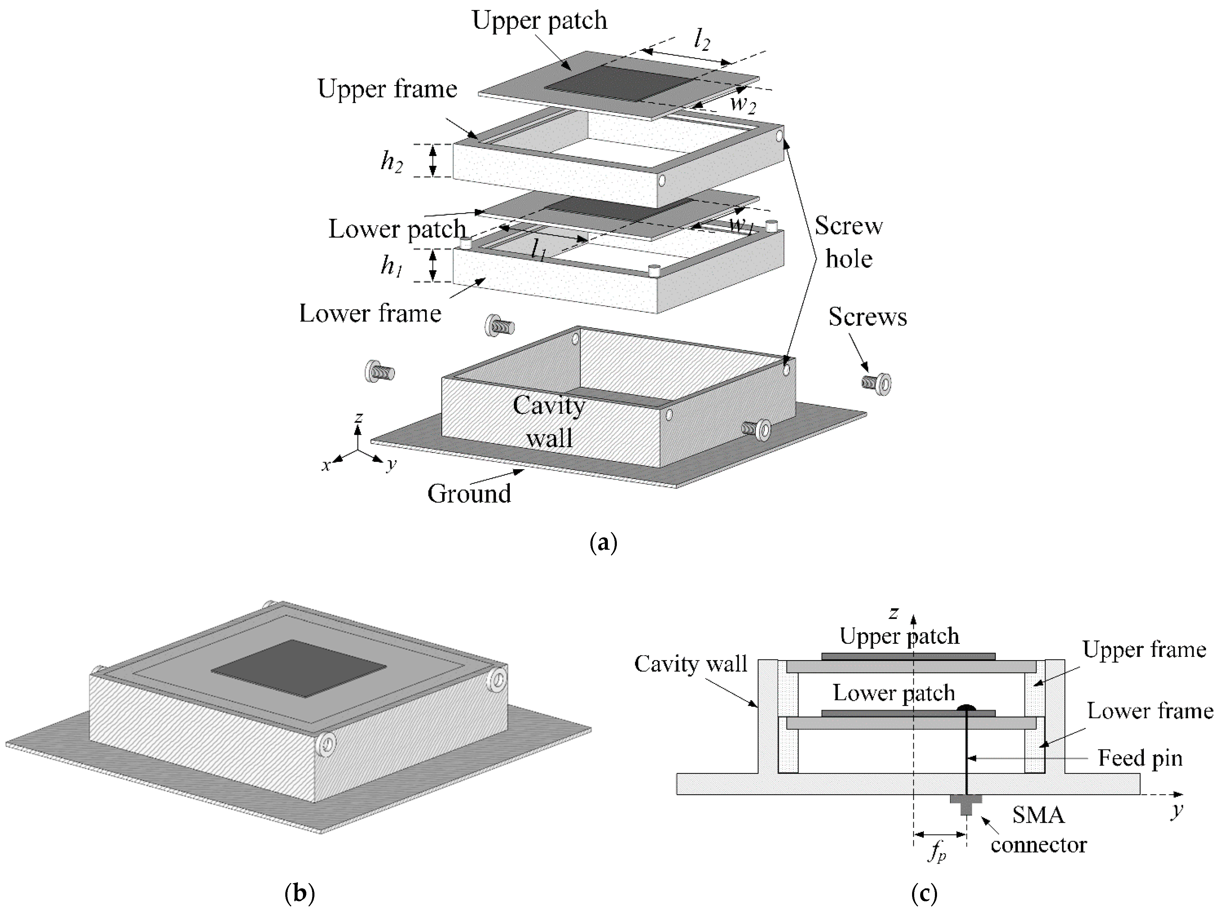
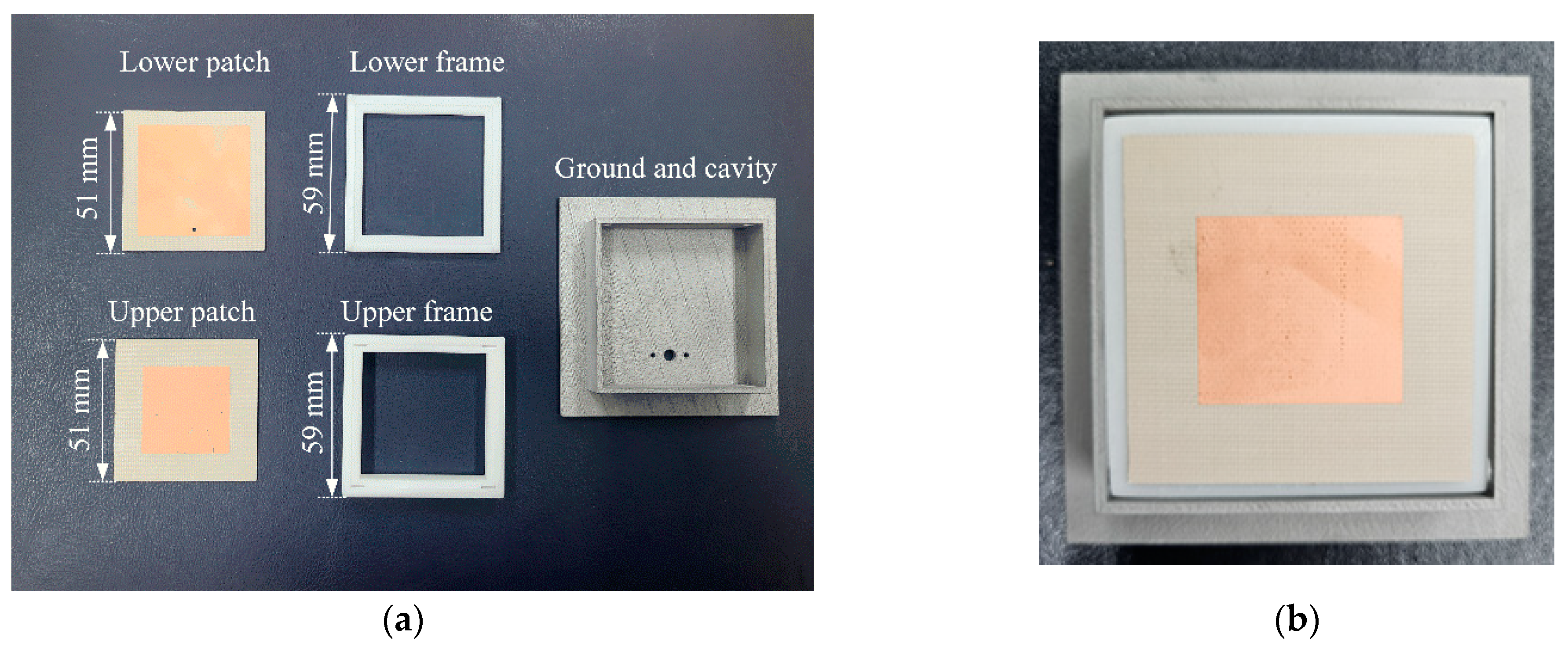
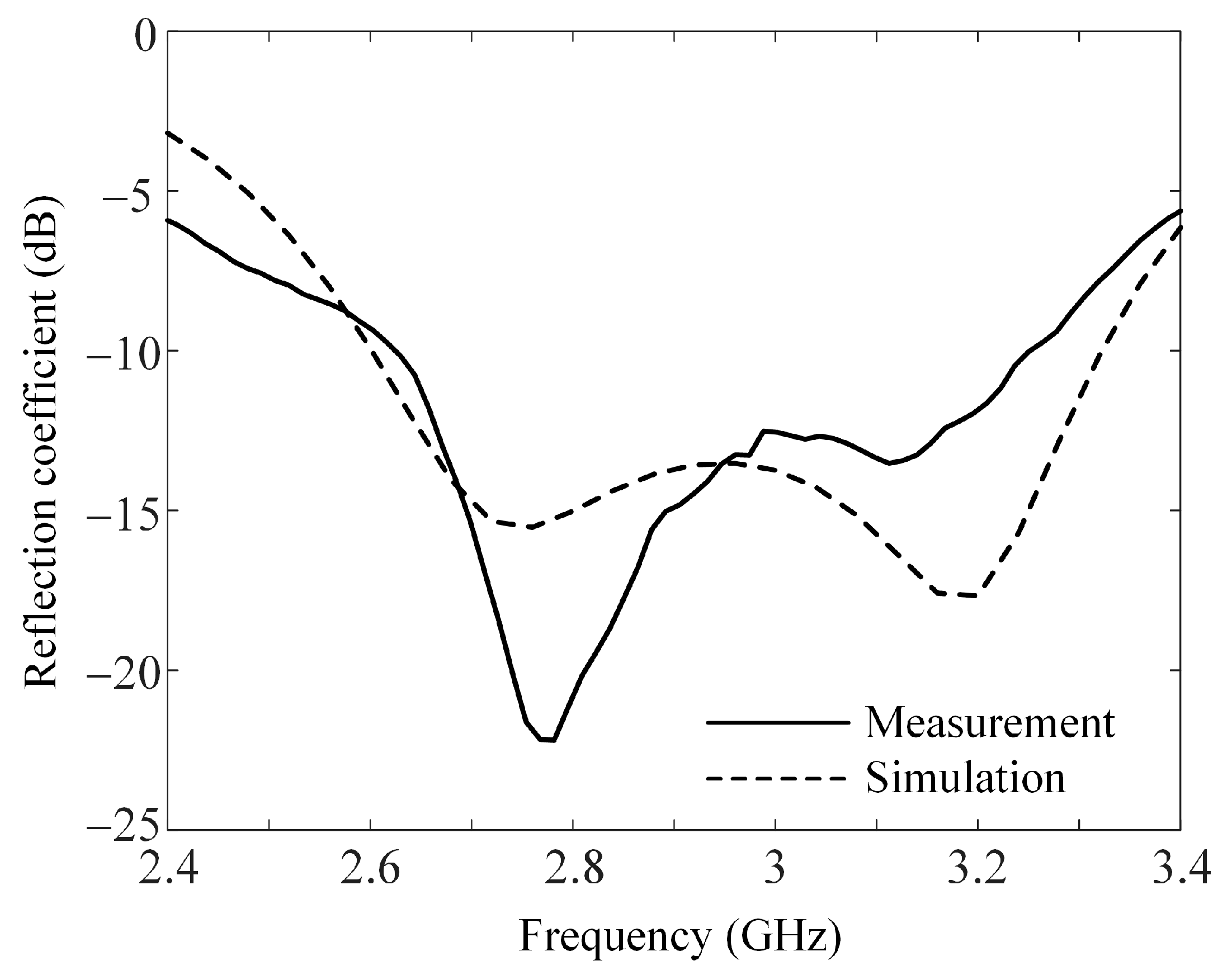
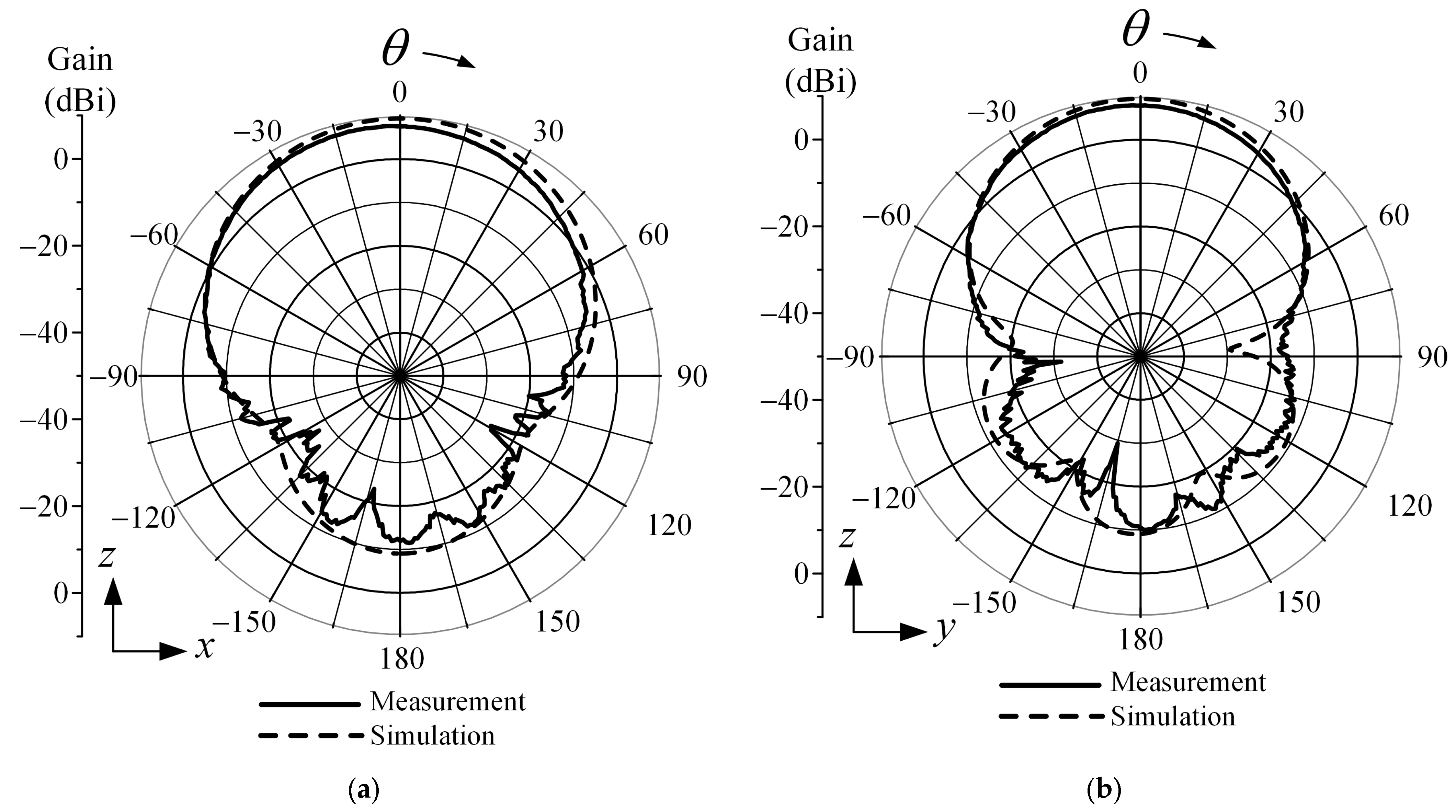
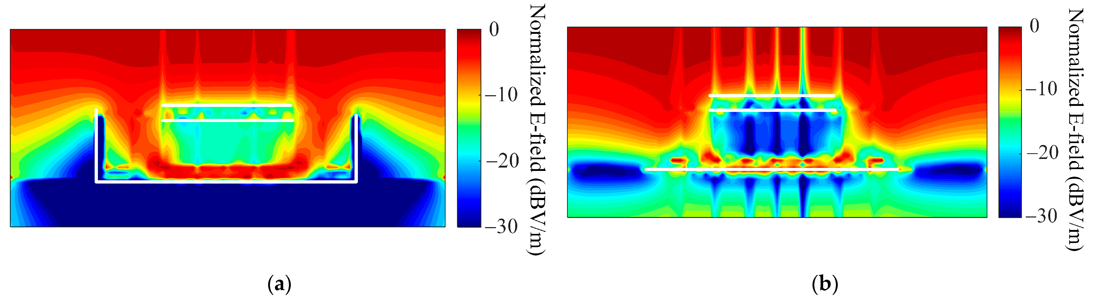
2. Design and Measurement of a Stacked Dual-Patch Antenna with Thick Quasi-Air Substrates

Figure 1 illustrates the geometry of the stacked dual-patch antenna with thick quasi-air substrates and a cavity wall. To achieve the theoretical maximum bandwidth of the patch antenna, the quality factor of the system should be minimized. In this study, two techniques are employed when designing the antenna components to reduce the quality factor of the system: one is to enlarge the area of the conductive radiator as much as possible, and the other is to reduce the permittivity of the substrate within the patch to close to 1. To enlarge the conductive radiator and realize a patch antenna with this maximum bandwidth, we applied the stacked dual-patch configuration to the proposed antenna design. This stacked dual-patch configuration consists of the lower and upper rectangular patches. The width and length of the lower patch are w1 and l1, respectively, and this lower patch is directly connected to the SMA connector, as shown in Figure 1a. The upper patch, with a width w2 and a length l2, is coupled-fed from the lower patch. Thus, the proposed antenna with two radiators can achieve broadband characteristics due to the broadened area of the conductive radiators. To further broaden the antenna bandwidth, thick quasi-air substrates with low permittivity close to 1 are employed between the two radiators and the ground plate. Typically, the quasi-air substrates are implemented using Rohacell (εr = 1.08) [5,19], but patch antennas fabricated with this material are soft and vulnerable to heat, so their durability is relatively poor. To simultaneously improve the durability and bandwidth of the antenna, square-pipe resin frames (εr = 2.9) are fabricated using a 3D printing method for implementing the quasi-air substrate structure. The square-pipe resin frame also consists of lower and upper frames, and the thicknesses of the lower and upper square-pipe resin frames are h1 and h2, respectively. Thus, the proposed quasi-air substrate has a low dielectric constant of 1.8. To increase the front-to-back ratio and suppress the leakage electric fields of the patch antenna, a metal cavity wall is placed around the square-pipe resin frame, as shown in Figure 1b. The geometrical parameters of the proposed antenna with the stacked dual-loop design are optimized using the FEKO electromagnetic simulator [20] and the genetic algorithm (GA) [21]. The optimum parameters are listed in Table 1. These geometrical parameters of the proposed antenna were determined in the following process: First, the initial values were obtained from the basic theory for the patch antenna [8]. For example, an antenna’s length is half of a wavelength (50 mm), and the thickness of the antenna is determined by less than 1/10 of a wavelength (10 mm). Next, these values are applied as the input to the GA, and the optimum design parameters are obtained through the GA. In this optimization process, a cost function is determined simply as 1/antenna bandwidth.
Figure 2 shows photographs of the fabricated antenna with thick quasi-air substrates and the cavity wall. The fabrication of the proposed antenna is carried out using the following procedures: First, two conductive radiators for the patch are printed on an RF-35 substrate (εr = 3.5, tan δ = 0.0018, thickness = 0.5 mm) using photolithography and etching techniques. Next, two square-pipe resin frames are built to realize the thick quasi-air substrates using the SLA 3D printing method [17] that can provide high-durability structures with low manufacturing tolerances. The metal cavity wall with the ground plate is then manufactured using the SLM 3D printing method [18] that can provide full-metal body structures with low manufacturing tolerances at a low cost. Finally, the stacked dual-patch antenna, the square-pipe resin frames, and the ground plate are assembled with a metal cavity wall to form a complete antenna structure. To verify the antenna’s feasibility, indicators of the antenna’s performance such as reflection coefficients, bore-sight gains, and radiation patterns are measured in a full anechoic chamber.
Figure 3 presents the reflection coefficient of the proposed antenna. The solid and dashed lines indicate measured and simulated results, respectively. The measured reflection coefficient has a bandwidth of 620 MHz (2.63 GHz to 3.25 GHz, |Γ|dB < −10 dB), with a fractional bandwidth of 20.7%. This result is in good agreement with the simulated fractional bandwidth of 24%. In addition, the average reflection coefficients of the measurement and simulation are −14.9 dB and −14.2 dB, respectively.
Figure 4 illustrates the 2D radiation gain patterns (in a spherical coordinate system) of the proposed antenna in the E-plane (zx-plane) and H-plane (zy-plane). At 3 GHz, the bore-sight gains of the measurement and simulation are 7.9 dBi and 8.9 dBi, respectively. In addition, the measured half-power beamwidths (HPBWs) in the E- and H-planes are 48° and 55°, respectively, while the simulated HPBWs are 56° and 52°.

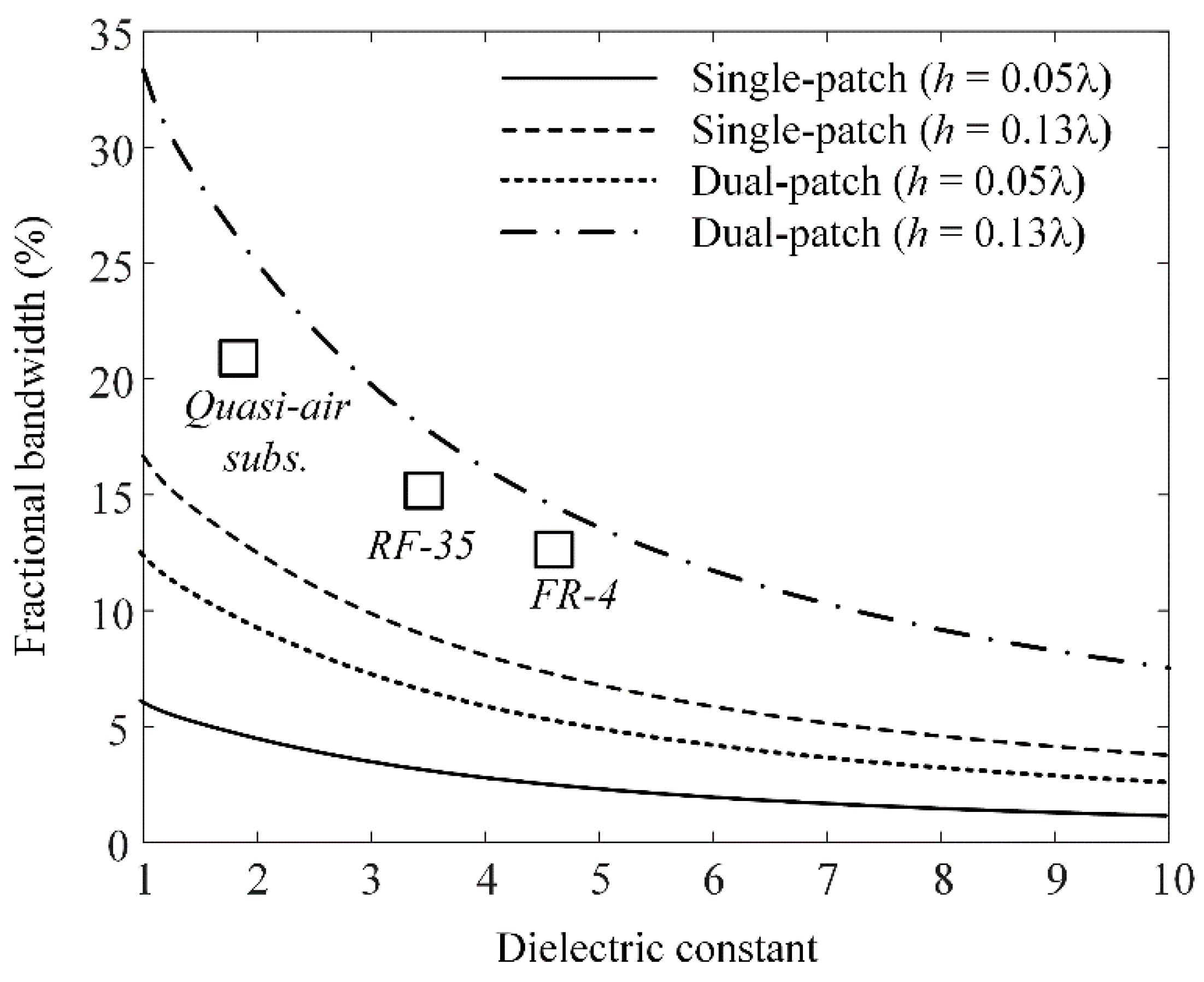
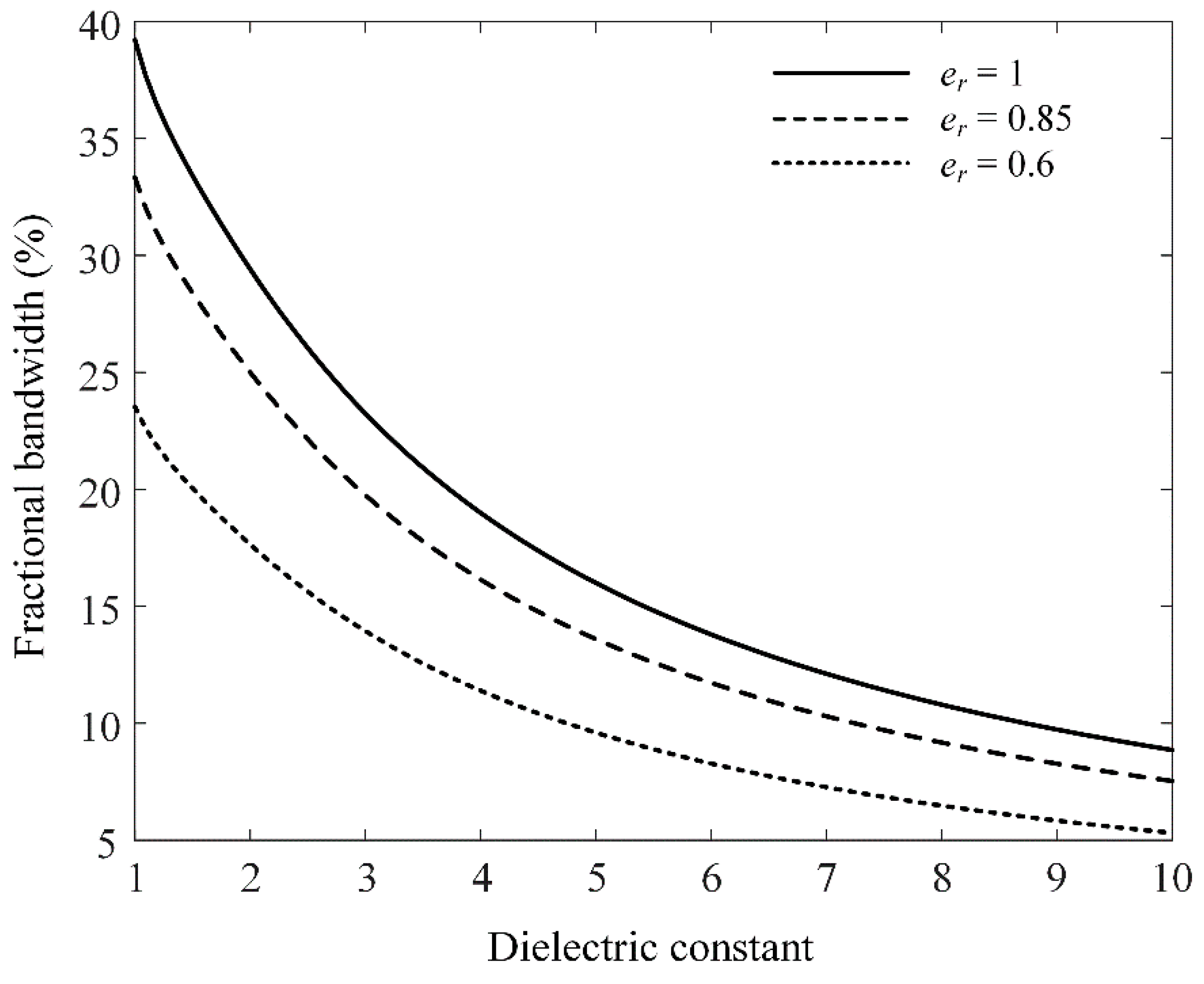
3. Analysis and Comparison with Fundamental Bandwidth Limit

Figure 5 presents the theoretical maximum bandwidth of the patch antenna according to the permittivity of the substrates. The bandwidth of the patch antenna can be calculated using the following equation [6,8]:
B W = V S W R 1 Q V S W R
where Q is the quality factor of the antenna. When the surface wave power of the patch antenna is much smaller than the radiated power, the expression for the bandwidth of the patch antenna can be approximated as follows [6,8]:
B W = 16 3 2 c 1 p e r 1 ε r h λ 0 W L
where er is the radiation efficiency of the patch antenna, and h is the total thickness of the substrate. p means the ratio of the power radiated by the patch to that radiated by an equivalent Hertzian dipole of the same moment. This p factor can be approximately 1.0 when the patch antenna has a small size [8]. W and L are the width and length of the conductive resonator of the patch antenna, and c1 is expressed as follows [6,8]:
c 1 = 1 1 n 2 + 2 / 5 n 4
where n is ε μ , and ε and μ are the permittivity and the permeability of the antenna substrates (the upper and lower substrate layers in the proposed antenna), respectively. According to Equations (1) and (2), in order to achieve the theoretical maximum bandwidth of the patch antenna, the quality factor of the system should be minimized. To do so, the area of the conductive radiator and the thickness of the substrate should be enlarged. In addition, the permittivity of the substrate in the patch should be minimized. The results in Figure 3 are then compared with the theoretical bandwidth calculated using Equation (2). The solid and dashed lines represent the theoretical maximum bandwidth of the patch antenna for which the thicknesses of the substrates are h = 0.05λ and h = 0.13λ, respectively. In this result, p and er are assumed to be 1 and 0.85, respectively, and the ratio of W and L is 1. The maximum bandwidth of the dual patch (dotted and dash-dotted lines) is assumed to be twice that of the single patch (solid and dashed lines), considering their two resonators. Therefore, the theoretical maximum bandwidth of the dual patch with the quasi-air substrate (εr = 1.8) is calculated to be 26%. In fact, the bandwidth of the simulation model for the proposed dual-patch antenna has a bandwidth of 21%. In addition, the fundamental bandwidth limits of the antennas with the RF-35 and FR-4 substrates are 15.5% and 13.3%, respectively. These results demonstrate that by using the proposed antenna structure, broadband characteristics close to the fundamental bandwidth limit of the patch antenna can be achieved, and at the same time, the durability of the antenna is improved for various applications.
Figure 6 represents the fundamental bandwidth limit of the dual-patch antenna (h = 0.13λ) according to the antenna’s efficiency [6,8]. As can be seen in this figure, when there is no reduction in bandwidth due to the antenna’s efficiency (er = 1), the fractional bandwidth of the antenna with the quasi-air substrate is 30.8%. On the other hand, when the antenna’s efficiency is reduced to 0.6, the bandwidth is also reduced to 18.5%.
Table 2 shows comparisons of the antenna’s characteristics with other stacked coupled-fed antennas. As can be seen in this table, the antennas in [5,13] with air foam substrates have a broad bandwidth while having a relatively low profile. In addition, an antenna in [11] achieved broader bandwidth through a shorted patch and an L-shaped probe structure. However, these antennas fabricated with air foam are soft and vulnerable to heat, so their durability is relatively poor. On the other hand, the proposed antenna with 3D printed quasi-air substrates achieved a broad bandwidth while demonstrating high durability.
Figure 7 shows the normalized electric field distributions of the antenna with and without the metal cavity at 3 GHz. As can be seen in Figure 7a, leakage electric fields that formed on the sides and back of the antenna are suppressed by the metal cavity structure. In contrast, without the metal cavity structure, a strong leakage electric field is observed around the antenna structure, as shown in Figure 7b.

4. Conclusions

In this paper, we investigated a stacked dual-patch antenna with 3D printed thick quasi-air substrates and a cavity wall for wideband applications. In order to achieve the theoretical maximum bandwidth of the patch antenna, a stacked dual-patch configuration was employed to the proposed antenna to extend the area of the conductive radiator. In addition, the square-pipe resin frames manufactured using the 3D printing method were applied to the proposed antenna to implement a quasi-air substrate structure that has a low permittivity close to 1. Therefore, the proposed antenna had a broad bandwidth of 620 MHz with a fractional bandwidth of 20.7%. Then, the bore-sight gain of the proposed antenna is 7.9 dBi, and the HPBWs in the E- and H-planes are 48° and 55°, respectively. The results demonstrate that by using the proposed antenna structure, broadband characteristics close to the fundamental bandwidth limit of the patch antenna can be achieved, and at the same time, the durability of the antenna can be improved for various applications such as military radar systems, mobile communication systems, and wireless transfer systems.

Author Contributions

Conceptualization, D.J., H.C., and J.-Y.L.; formal analysis, D.J. and H.C.; funding acquisition, H.C.; investigation, D.J. and J.-Y.L.; methodology, D.J. and J.-Y.L.; project administration, H.C.; software, D.J. and J.-Y.L.; supervision, H.C.; validation, D.J., J.-Y.L., and H.C.; visualization, D.J.; writing—original draft, D.J.; writing—review and editing, D.J., J.-Y.L., and H.C. All authors have read and agreed to the published version of the manuscript.

Funding

This work was supported by Korea Research Institute for defense Technology planning and advancement (KRIT) grant funded by the Korea government (DAPA (Defense Acquisition Program Administration)) (No. KRIT-CT-22-021, Space Signal Intelligence Research Laboratory, 2022).

Institutional Review Board Statement

Not applicable.

Informed Consent Statement

Not applicable.

Data Availability Statement

Data are contained within the article.

Conflicts of Interest

The authors declare no conflict of interest.

References

  1. Huang, H.; Li, X.; Liu, Y. A low-profile, dual-polarized patch antenna for 5G MIMO application. IEEE Trans. Antennas Propag. 2019, 67, 1275–1279. [Google Scholar] [CrossRef]
  2. Bilgic, M.M.; Yegin, K. Modified annular ring antenna for GPS and SDARS automotive applications. IEEE Antennas Wirel. Propag. Lett. 2015, 15, 1442–1445. [Google Scholar] [CrossRef]
  3. Kim, H.Y.; Lee, Y.; Nam, S. Efficiency bound estimation for a practical microwave and mmWave wireless power transfer system design. J. Electromagn. Eng. Sci. 2023, 23, 69–74. [Google Scholar] [CrossRef]
  4. Yoo, S.; Milyakh, Y.; Kim, H.; Hong, C.; Choo, H. Patch array antenna using a dual coupled feeding structure for 79 GHz automotive radar applications. IEEE Antennas Wirel. Propag. Lett. 2020, 19, 676–679. [Google Scholar]
  5. Nasimuddin; Esselle, K.P.; Verma, A.K. Wideband circularly polarized stacked microstrip antenna. IEEE Antennas Wirel. Propag. Lett. 2007, 6, 21–24. [Google Scholar] [CrossRef]
  6. Balanis, C.A. Antenna Theory: Analysis and Design, 4th ed.; John Wiley & Sons, Inc.: Hoboken, NJ, USA, 2016. [Google Scholar]
  7. Jiang, H.; Yan, N.; Ma, K.; Wang, Y. A wideband circularly polarized dielectric patch antenna with a modified air cavity for Wi-Fi 6 and Wi-Fi 6E applications. IEEE Antennas Wirel. Propag. Lett. 2023, 22, 213–217. [Google Scholar] [CrossRef]
  8. Jackson, D.R.; Alexopoulos, N.G. Simple approximate formulas for input resistance, bandwidth, and efficiency of a resonant rectangular patch. IEEE Trans. Antennas Propag. 1991, 39, 407–410. [Google Scholar] [CrossRef]
  9. Fan, K.; Hao, Z.-C.; Yuan, Q. A low-profile wideband substrate-integrated waveguide cavity-backed E-shaped patch antenna for the Q-LINKPAN applications. IEEE Trans. Antennas Propag. 2017, 65, 5667–5676. [Google Scholar] [CrossRef]
  10. Li, W.; Xue, W.; Li, Y.; Chung, K.L.; Huang, Z. A Wideband differentially fed circularly polarized slotted patch antenna with a large beamwidth. J. Electromagn. Eng. Sci. 2023, 23, 512–520. [Google Scholar] [CrossRef]
  11. Jang, D.; Yoo, S.; Wang, J.; Choo, H. Design of a 16-element array antenna with a planar L-shaped probe for a direction of arrival estimation of the unidentified broadband signal. Microw. Opt. Technol. Lett. 2019, 61, 2315–2322. [Google Scholar] [CrossRef]
  12. Liang, Z.; Liu, J.; Li, Y.; Long, Y. A dual-frequency broadband design of coupled-fed stacked microstrip monopolar patch antenna for WLAN applications. IEEE Antennas Wirel. Propag. Lett. 2015, 15, 1289–1292. [Google Scholar] [CrossRef]
  13. Herscovici, N.; Sipus, Z.; Bonefacic, D. Circularly polarized single-fed wide-band microstrip patch. IEEE Trans. Antennas Propag. 2003, 51, 1277–1280. [Google Scholar] [CrossRef]
  14. Wang, S.; Zhang, X.; Zhu, L.; Wu, W. Single-fed wide-beamwidth circularly polarized patch antenna using dual-function 3-D printed substrate. IEEE Antennas Wirel. Propag. Lett. 2018, 17, 649–653. [Google Scholar] [CrossRef]
  15. Muntoni, G.; Montisci, G.; Casula, G.A.; Chietera, F.P.; Michel, A.; Colella, R.; Catarinucci, L.; Mazzarella, G. A curved 3-D printed microstrip patch antenna layout for bandwidth enhancement and size reduction. IEEE Antennas Wirel. Propag. Lett. 2020, 19, 1118–1122. [Google Scholar] [CrossRef]
  16. Wang, S.; Zhu, L.; Wu, W. 3-D printed inhomogeneous substrate and superstrate for application in dual-band and dual-CP stacked patch antenna. IEEE Trans. Antennas Propag. 2018, 66, 2236–2244. [Google Scholar] [CrossRef]
  17. Mhmood, T.R.; Al-Karkhi, N.K. A review of the stereo lithography 3D printing process and the effect of parameters on quality. Al-Khwarizmi Eng. J. 2023, 19, 82–94. [Google Scholar] [CrossRef]
  18. Ohm, S.; Kang, E.; Lim, T.H.; Choo, H. Design of a dual-polarization all-metal Vivaldi array antenna using a metal 3D printing method for high-power jamming systems. IEEE Access 2023, 11, 35175–35181. [Google Scholar] [CrossRef]
  19. Vague, J.; Melgareho, J.C.; Guglielmi, M.; Boria, V.E.; Anza, S.; Vicente, C.; Moreno, M.R.; Taroncher, M.; Martinez, B.G.; Raboso, D. Multipactor effect characterization of dielectric materials for space applications. IEEE Trans. Microw. Theory Tech. 2018, 66, 3644–3655. [Google Scholar] [CrossRef]
  20. FEKO EM Software. Altair. Available online: https://www.altair.co.kr/feko/ (accessed on 1 November 2023).
  21. Hassanat, A.; Almohammadi, K.; Alkafaween, E.; Abunawas, E.; Hammouri, A.; Surya Prasath, V.B. Choosing mutation and crossover ratios for genetic algorithms—A review with a new dynamic approach. Information 2019, 10, 390. [Google Scholar] [CrossRef]
Figure 1. Geometry of the proposed antenna: (a) isometric view of each antenna component; (b) isometric view of the assembled antenna; (c) side view of the assembled antenna.
Applsci 14 01571 g001
Figure 2. Photographs of the fabricated antenna: (a) each component of the antenna; (b) assembled antenna.
Applsci 14 01571 g002
Figure 3. Reflection coefficient of the proposed antenna.
Applsci 14 01571 g003
Figure 4. Radiation pattern of the proposed antenna: (a) zx-plane; (b) zy-plane.
Applsci 14 01571 g004
Figure 5. Fundamental bandwidth limit of the patch antenna according to the dielectric constant.
Applsci 14 01571 g005
Figure 6. Fundamental bandwidth limit of the patch antenna according to the antenna efficiency.
Applsci 14 01571 g006
Figure 7. Near-field distributions with and without the cavity: (a) with the cavity; (b) without the cavity.
Applsci 14 01571 g007
Table 1. Geometrical parameters of the proposed antenna.
ParametersValueParametersValue
w128.4 mmw227 mm
l140.3 mml226.7 mm
h12.4 mmh210.2 mm
fp19.3 mm
Table 2. Comparison with other stacked coupled-fed antennas.
ResearchSubstrateBandwidthAntenna HeightDurability
[5]Air foam
(εr = 1.07)
21%0.085λPoor
[13]Air foam
(εr = 1.05)
20%0.085λPoor
[11]Air foam
(εr ≈ 1)
41%0.094λPoor
ProposedQuasi-air
(εr = 1.8)
21%0.13λGood
Disclaimer/Publisher’s Note: The statements, opinions and data contained in all publications are solely those of the individual author(s) and contributor(s) and not of MDPI and/or the editor(s). MDPI and/or the editor(s) disclaim responsibility for any injury to people or property resulting from any ideas, methods, instructions or products referred to in the content.

