1. Introduction
The phenomenon of surface charging induced by mutual contact and friction between materials is referred to as contact electrification or triboelectrification [
1,
2,
3,
4,
5]. This process involves the transfer of charges, leading to the accumulation of charges of different polarities and densities on the surface of objects, resulting in electrostatic effects. Although static electricity plays a positive role in various fields such as electrostatic dust removal [
6,
7,
8,
9], electrostatic spraying [
10,
11,
12,
13], electrostatic flocking [
14,
15,
16,
17], and electrostatic copying [
18,
19], the accumulation discharge of charges and electrostatic attraction also pose significant hazards. For example, electrostatic discharge may cause electromagnetic interference and circuit breakdown in electronic devices [
20,
21], high-voltage electrostatic discharge poses a threat to personal safety [
22], and electrostatic discharge in dusty environments may lead to explosions and fires [
23,
24,
25]. Additionally, dust adhesion caused by electrostatic attraction can significantly reduce the quality of industrial products [
26]. Therefore, precise measurement of the surface charge density of objects becomes crucial for better understanding and controlling electrostatic effects, achieving safer, more efficient, and reliable applications.
Currently, various methods exist for measuring the surface charge density of materials. Wang et al. [
27] utilized electrostatic induction to derive the relationship between the contact separation distance and the surface charge density by measuring the voltage of the circuit during the contact separation process. Furthermore, by measuring the voltage of the same liquid metal after the contact separation with the tested material, the contact electrification charge density of different materials for the same material can be inferred. The Faraday cup method records the change in current when the tested material enters the Faraday cup through electrostatic induction to calculate the quantity of charge, thereby obtaining the charge density [
28,
29]. The aforementioned methods provide the average surface charge density of materials and cannot reveal the distribution characteristics of charge density on the surface. Electrostatic field strength meters can measure electric field strength, which can then be used to deduce the charge distribution [
30]. This method does not require direct contact with the material, thus avoiding interference with the tested material. However, the spatial resolution of electrostatic field strength meters is often limited and cannot accurately calculate the surface charge density of materials.
In 1898, Lord Kelvin invented a technique for measuring the contact potential difference of metals, known as the Kelvin method [
31]. In 1932, Zisman optimized this method by designing circuits to make it more sophisticated and accurate [
32,
33,
34,
35]. The Kelvin method is also known as the vibrating capacitor method. In this method, the contact potential difference between two metals is generated due to the different work functions of the metals [
36,
37,
38]. A capacitor is formed between the probe and the tested metal, and by applying vertical vibration to the probe perpendicular to the test surface, the contact potential difference induces a weak current in the measuring circuit. Applying a certain bias voltage to the probe ensures no current flows in the measuring circuit. At this point, the probe-to-ground voltage equals the material’s contact potential difference. Later, the vibrating capacitor method was used to measure the surface potential of dielectric materials. As the probe size decreased, the spatial resolution of surface potential measurement improved. Subsequently, the Kelvin method was combined with Atomic Force Microscopy (AFM) technology, gradually developing into Kelvin Probe Force Microscopy (KPFM) technology, achieving atomic-level spatial resolution in surface potential measurement. In KPFM technology, by applying DC and AC biases to the probe, the DC bias is used to compensate for the surface potential of the sample, while the AC bias generates changing electrostatic forces to make the probe vibrate. When the second harmonic amplitude of the probe is zero, the DC bias applied to the probe equals the surface potential of the material.
Currently, the vibrating capacitor method can achieve non-contact and non-destructive measurement of surface potential with high spatial resolution, serving as the theoretical basis for many commonly used surface potential measurement devices. However, the vibrating capacitor method was originally designed to detect the contact potential difference or differences in work functions of samples. During the measurement process, the stable current parameters ensure that the applied bias voltage strictly equals the potential difference between the tested metal and the reference voltage. However, unlike conductors, dielectric materials do not have a fixed and uniform surface potential. In addition to being related to surface charge polarity, density, and other conditions, the surface potential of dielectric materials is also influenced by factors such as probe size, probe position, and probe bias voltage [
39,
40,
41,
42]. Conversely, due to their extremely low conductivity, the surface charge distribution of dielectric materials often remains stable. Therefore, the surface potential of dielectric materials does not have physical significance; what can be stably measured is their surface charge density. However, so far, the quantitative relationship between the surface potential measurement values obtained by the vibrating capacitor method and the surface charge density remains unclear, affecting the accurate measurement of surface charge density of dielectric materials.
This study proposes a method based on Comsol simulations to establish the relationship between surface charge and measured voltage for dielectric materials, while simplifying the simulation process through integration calculation. The aim of this paper is twofold: firstly, to establish an ideal parallel plate capacitor theoretical model and derive the theoretical relationship between surface charge density and measured potential. Additionally, the study aims to create two-dimensional and three-dimensional simulation models of the vibrating capacitor method measurement process. It also investigates the influence of factors such as charged area and probe height on the measured potential using COMSOL Multiphysics 5.6. Lastly, the study seeks to establish an analytical relationship between the measured potential value and the surface charge density distribution. This is based on the potential measurement model of surface point charge distribution. The feasibility of integration calculation as an alternative to simulation methods is then validated using various charge density distributions, including circular trajectory sinusoidal distribution, circular trajectory random distribution, square region random distribution, and others.
3. Results and Discussion
3.1. Theoretical Model of Parallel Plate Capacitor
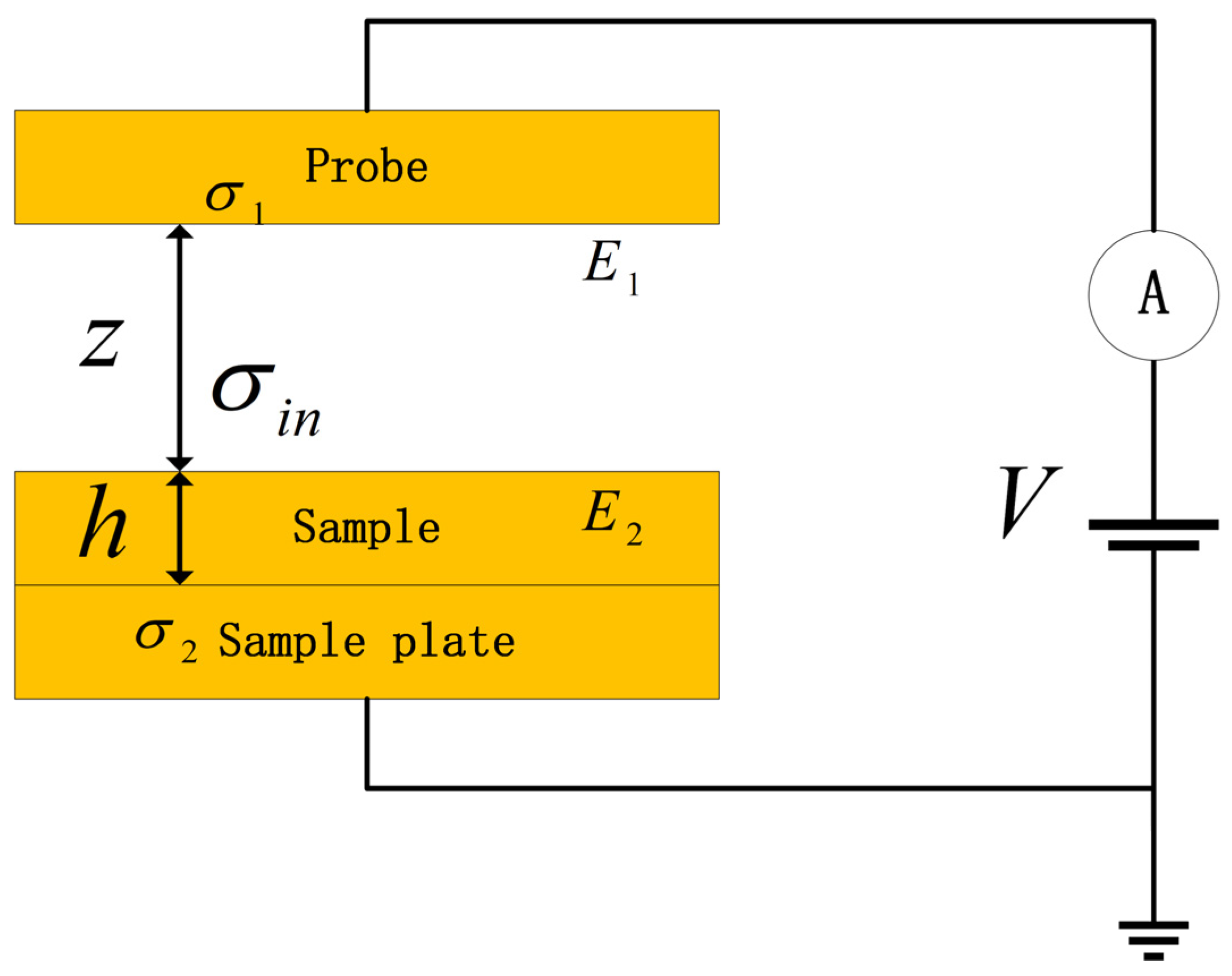
Based on the principle of the vibrating capacitor method, a theoretical model is established, as shown in
Figure 3.
represents the surface charge density of the dielectric material sample, caused by phenomena such as frictional charging, and remains unaffected by other variables during the measurement process.
denotes the induced surface charge density on the lower surface of the upper metal plate (probe) after applying the input voltage, while
represents the surface charge density induced on the lower metal plate (sample holder) and the lower surface of the insulating material sample.
In addition, let z denote the distance between the lower surface of the probe and the upper surface of the sample, and h represent the thickness of the sample being measured. E1 represents the magnitude of the electric field between the probe plates, while E2 denotes the electric field within the sample. V represents the voltage output from the voltage source, and A denotes the inclusion of an ammeter in series within the circuit.
Therefore, in electrostatic equilibrium, the applied voltage provided by the external circuit satisfies the following equation for potential measurement. In the equation,
ε0 represents the vacuum permittivity and
εr represents the relative permittivity of the dielectric material:
By adjusting the magnitude of the potential measurement to ensure that the current in the circuit is zero, we achieve:
At this point, the relationship between the surface charge density of the material and the potential measurement is:
Formula (4) represents the relationship between the surface charge density of the sample and the measured voltage in the ideal state of the parallel plate capacitor model.
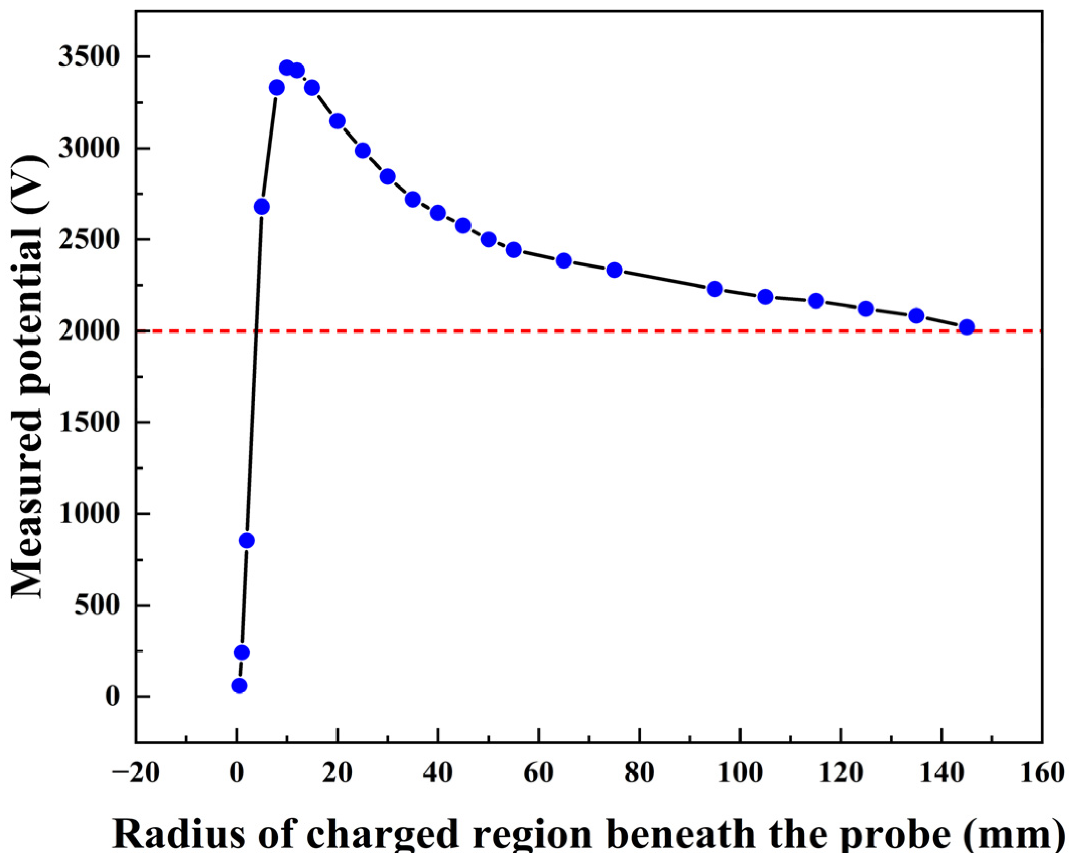
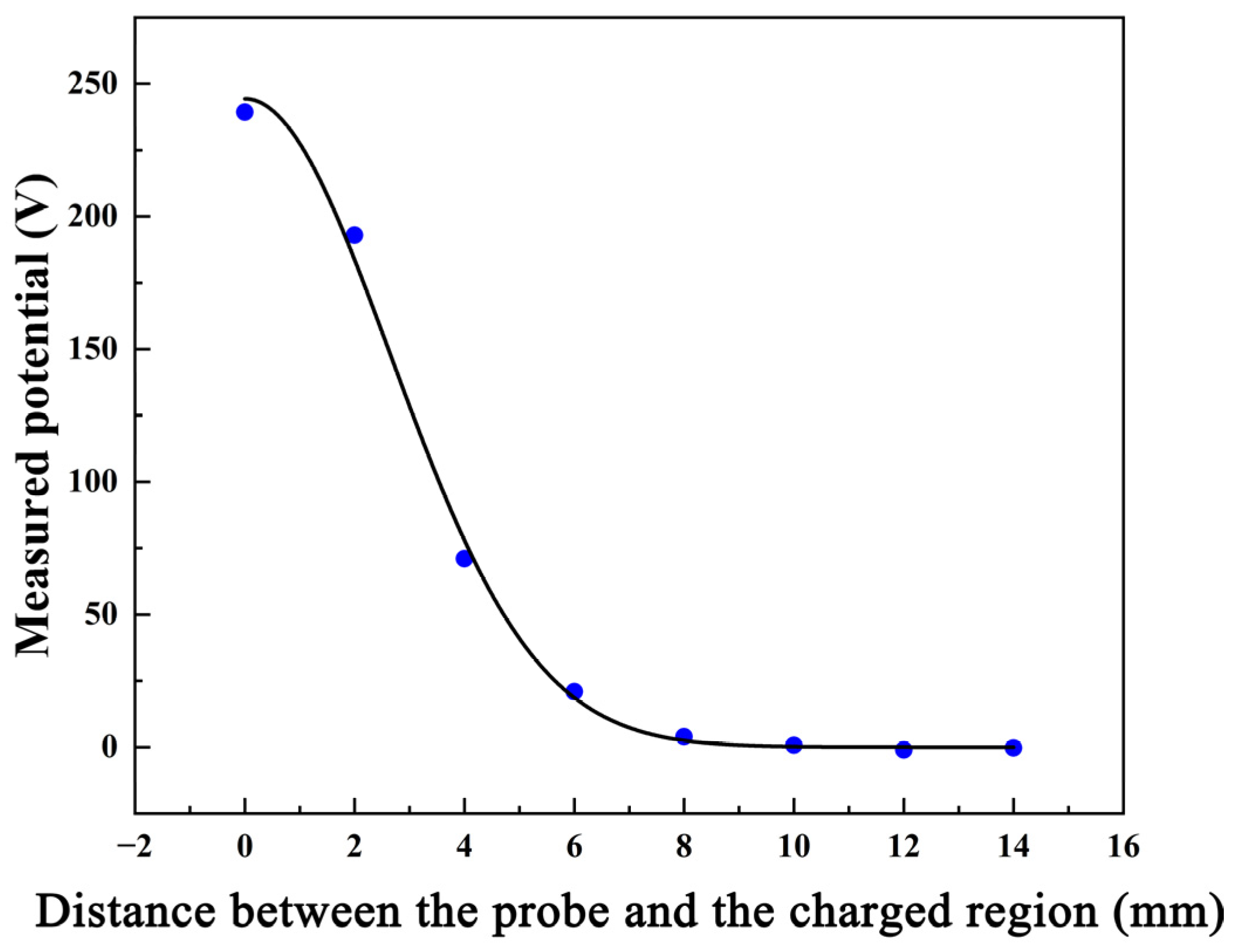
3.2. Relationship between Measured Potential and Charged Area
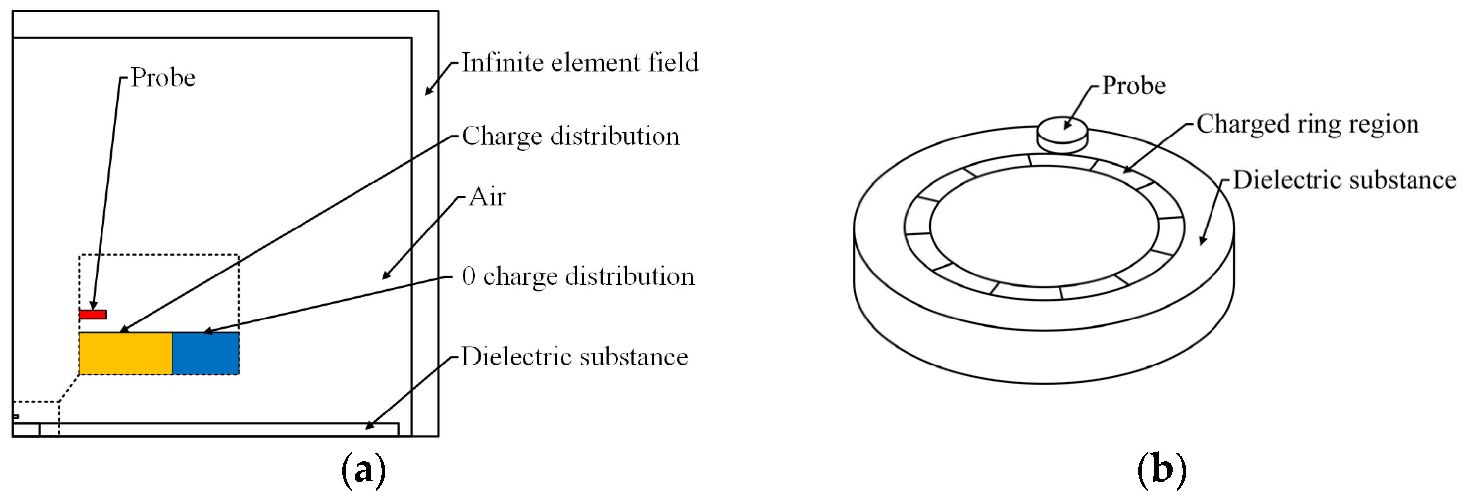
When the tested material is a dielectric substance, due to its low conductivity, surface charges adhere to the material surface. Different measured potentials exist at different distances between the probe and the charges. Therefore, by establishing a two-dimensional axisymmetric model as shown in
Figure 1a, with the lower surface of the probe maintained at a distance of 2 mm from the upper surface of the tested material, when the surface charge density of the charged region is set to 7.08 × 10
−6 C/m
2 as
σex, the results, as shown in
Figure 4, indicate that the measured potential rapidly increases within a radius of 10 mm as the charged area gradually increases from a radius of 0.5 mm to the entire lower surface with a radius of 145 mm uniformly distributing positive charges. When the radius of the charged area is 10 mm, the measured potential value approaches a peak of 3438.75 V. After the radius of the charged area exceeds 10 mm, the measured potential gradually decreases, reaching close to 2000 V as the charged radius reaches its maximum. According to Formula (4) in the parallel plate capacitor model, it can be calculated that the measured voltage is 2000 V when the lower surface of the tested material carries the currently set surface charge density under ideal conditions. It can be observed that the measured potential in the simulation experiment gradually approaches the theoretical value as the radius of the charged area increases. Furthermore, it is found that when the charge density is constant, the measured potential of the area with a radius of 10 mm is significantly greater than that of the entire lower surface with uniformly distributed charges. We speculate that this phenomenon, where a region with a smaller charge quantity exhibits a larger measured potential, is due to edge effects caused by uneven electric field line distribution.
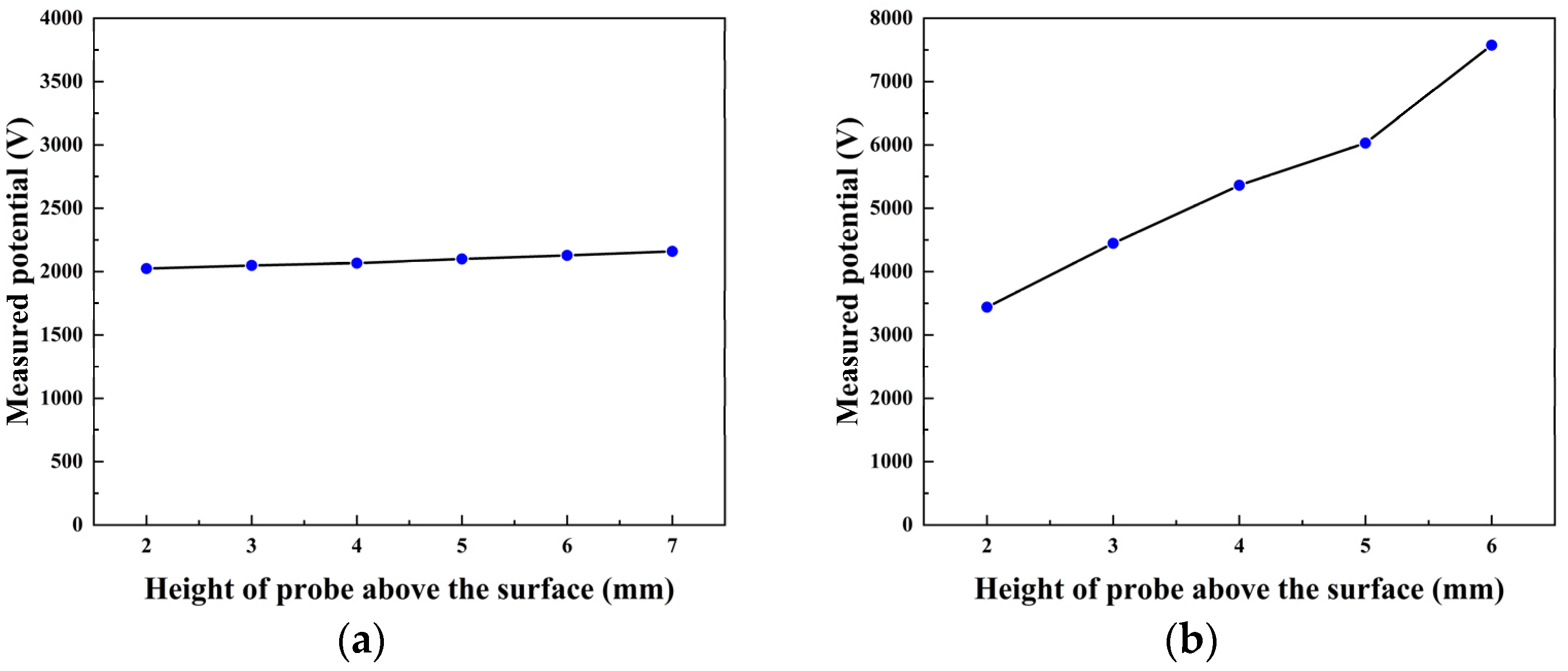
3.3. Relationship between Measured Potential and Probe Height
According to the principle of the vibrating capacitor method, for conductors, theoretically, the measured potential does not change with variations in the probe height. However, when the tested material is a dielectric substance, there is no clear correspondence between the material surface charge and the measured potential. Therefore, in the two-dimensional axisymmetric model, the entire upper surface of the tested material is uniformly charged with
σex and the edge of the tested material approaches an infinite domain. The distance between the lower surface of the probe and the sample is gradually adjusted. As shown in
Figure 5a, it can be observed that the measured potential remains stable at around 2000 V as the distance between the probe and the sample increases from 2 mm to 7 mm. Thus, under ideal conditions, when the charged region attached to the tested material approaches infinity, the measured potential of this model is not affected by changes in the probe height. However, for dielectric materials, charges can stably adhere to fixed positions. When the region below the probe is a charged area with a radius of 10 mm and a charge density of
σex, the measured potential exhibits a stable linear relationship as the distance between the probe and the sample increases from 2 mm to 6 mm, as shown in the following figure. This indicates that for dielectric materials under ideal conditions, the vibrating capacitor method model requires strict limitation of the probe height.
3.4. Relationship between Measured Potential and Charge Density Distribution
During the process of measuring surface potential using the vibrating capacitor method, the measured potential may be influenced by surface charges outside the measurement position. In order to establish the relationship between measured potential and surface charge density, simulations are first conducted to calculate the measured potentials at different positions under a point charge density distribution. Considering the influence of probe height on the surface charge of dielectric materials, the distance between the probe and the material surface is strictly maintained at 2 mm. Surface charges at different distances will result in different measurement values of potential. Therefore, in the three-dimensional model, a circular point charge area with a diameter of 1 mm is established at the center of the surface of the dielectric material. The probe is gradually moved horizontally from directly above the initial point charge area, with each movement being 2 mm. The results are shown in
Figure 6.
It can be observed that as the probe gradually moves away from the tested charged area, the measured potential of the probe rapidly decreases and approaches 0 volts. Through fitting, we can obtain the formula for the measured potential value
as a function of the horizontal distance
x between the center of the probe and the center of the charged area as follows:
After normalization, the formula can be derived as follows, where
r in the equation represents the linear distance between the tested unit charge and the center of the probe.
where
r in the equation represents the linear distance between the tested unit charge and the center of the probe. The relationship between the linear distance and the horizontal distance
x and the vertical distance y is as follows:
When the probe is placed above any charged region, the measured potential values for different charged regions can be calculated using the formula:
The term V (x, y) in the equation represents the measured voltage at the unit coordinates (x, y), while σ (x′, y′) denotes the magnitude of the surface charge density at the coordinates (x′, y′). The measured potential value at the current position can be obtained by performing the integration calculation of the charged region using the above formula based on the surface charge density under different conditions.
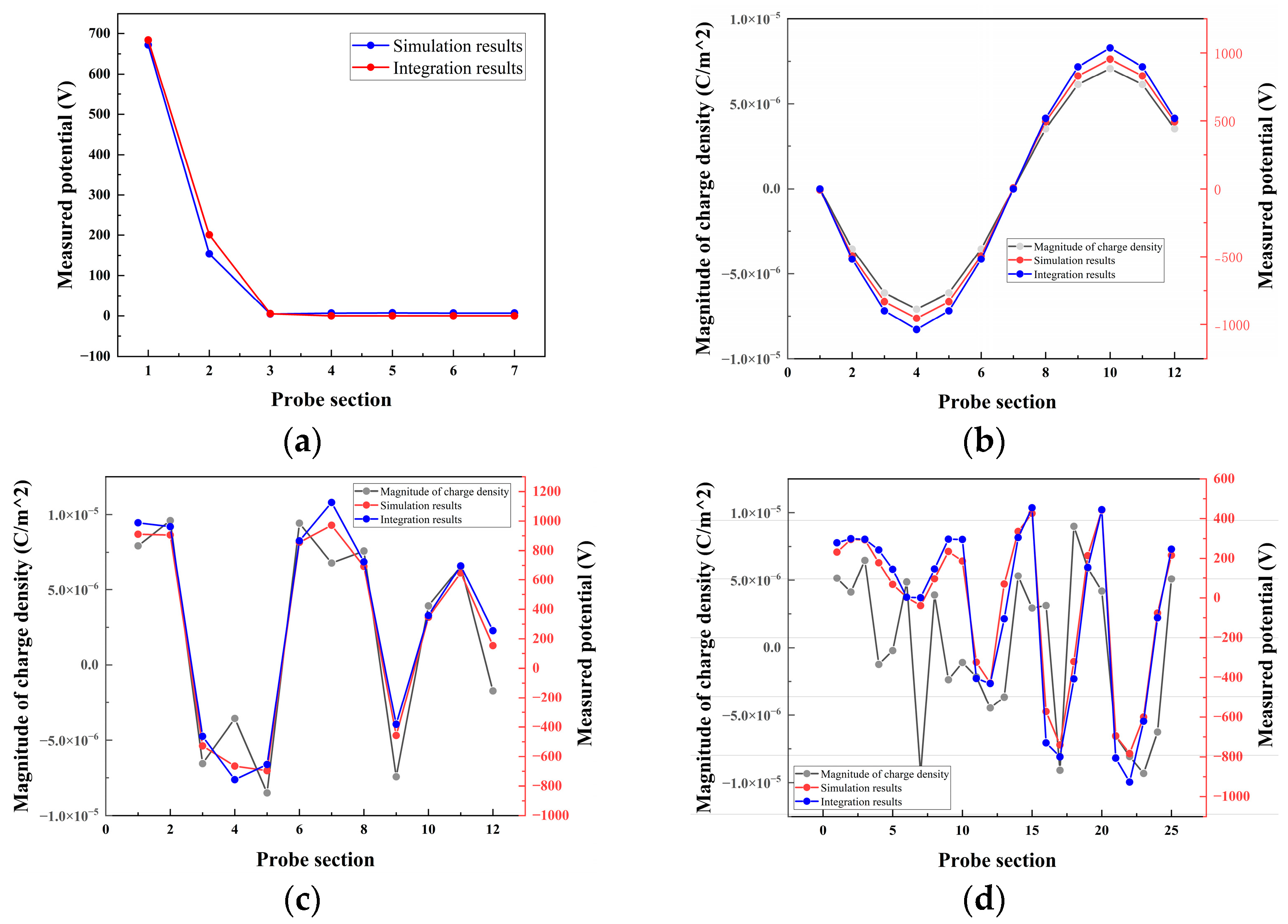
3.5. Validation of Different Types of Charge Density Distributions
Various scenarios of charge distribution have been investigated to validate distinct charging models. For example, during material contact and separation, surface charges often exhibit point-like characteristics. In our friction experiments, periodic friction along a circular trajectory may yield sinusoidal voltage measurements. Moreover, charges confined within localized regions may display random distribution properties. Through the examination of these diverse scenarios, our objective is to evaluate the feasibility of employing integration calculations as an alternative to simulation methods.
For the point charge region within the circular ring friction area, one of the 12 regions in
Figure 1b is selected to set the surface charge density to
σex, while the remaining regions are set to 0 C/m
2. The probe initially moves away from the charged region to other regions.
The results are shown in
Figure 7a: The x-coordinate of the probe section represents the position of the probe. As shown in
Figure 1b, when the probe is directly above the charged region, the x-value is 1. When the probe is positioned above an adjacent region next to the charged region, the x-value is 2, and so on. Since only one region is charged, and the entire model exhibits symmetry, it is only necessary to measure half of the circular ring area; namely, probe section 1 to 7. It can be seen that as the probe moves away from the charged region, the measured potential rapidly decreases and gradually approaches 0 V. Moreover, the simulation results of the model are close to the results of the integration calculation. In tribological experiments, after repeated cyclic friction in circular regions, measurements of surface charge along the friction trajectory exhibit characteristics reminiscent of sinusoidal signals.
When the charge distribution characteristic is similar to the friction experiment, surface charge densities with sinusoidal distribution characteristics are sequentially set in the 12 regions in
Figure 1b. The probe measures each charged region in sequence. The results, as shown in
Figure 7b, demonstrate that the simulation model results are very close to the numerical results obtained from the integrated calculations.
For the case of charges randomly distributed on the surface of the dielectric material, 12 random numbers representing the surface charge density in each subregion of the circular ring area are generated. The corresponding measured potentials are solved using both simulation methods and formula integration calculations, as shown in
Figure 7c. The gray line represents the randomly generated surface charge density values below the probe area, while the red and blue lines represent the simulated measured potential values obtained using the Comsol model and the calculated values obtained using the formula, respectively. Although there may be some fluctuations in situations where the surface charge density varies greatly, the curves obtained from both methods are generally consistent with the characteristics of the surface charge density distribution. The calculated values are similar to the simulated values in terms of characteristics, and the numerical values are also close.
However, it is more typical for material surfaces to exhibit irregular and non-uniform surface charges. Hence, in the modified configuration illustrated in
Figure 1b, the circular regions with charge are omitted and, instead, the central area of the upper surface is partitioned into 25 square regions with side lengths of 2 mm, forming a 5 × 5 grid. Random numbers are then generated to denote the surface charge density within these 25 regions. Subsequently, the probe systematically scans from directly above the first square to directly above the last square. The resultant measured potentials, obtained through both model simulations and formulaic computations, are depicted in
Figure 7d. On the
x-axis, the probe’s position is represented by grid numbers, starting from 1 when situated above the initial grid and incrementing sequentially until 25 as the probe traverses the grid. The
y-axis denotes the measured voltage corresponding to the probe’s position above the current grid. The gray line signifies the randomly generated surface charge density values beneath the probe area, while the red and blue lines respectively denote the simulated measured potential values derived from the simulation model and the calculated values obtained using the formula.
Observations from the graphical representations indicate that, for instances where the charge distribution exhibits relatively simple characteristics, such as point charge or sinusoidal distribution, the measured voltages obtained through integration calculations closely mirror those derived from simulations, with a minor numerical variance of approximately 50 V. However, in scenarios featuring more random charge distributions, while the measured voltages obtained through integration calculations demonstrate similar characteristics to simulation results, there are notable numerical differences, reaching approximately 100 V. Nevertheless, the overall trends in the measured voltages from both methods remain consistent. Notably, increasing the granularity of partitioning within the charged region may potentially yield more precise outcomes, as it enhances the model’s ability to capture nuanced features of the charge distribution, thus reducing discrepancies in measured voltages. However, it is important to emphasize that while greater partitioning may enhance accuracy, the primary focus of this study remains the proposition of a method leveraging integration calculations to optimize complex simulations, thereby achieving computational cost savings.
4. Conclusions
This research successfully addressed the challenge of measuring surface charge density in insulating materials using Comsol simulation methods. By analyzing parameters such as charged area size, probe height, and position, and utilizing the spatial distribution of potential measurement values of surface point charges, an integral relationship closely associated with the distribution of surface charge density was established. Validation against numerical simulation results from four common charge distribution scenarios confirmed the feasibility of using this integral relationship calculation method to replace complex electrostatic field simulation processes for determining the relationship between surface charge density and measured voltage. Additionally, this method provides a reliable approach for measuring surface charge density in insulating materials. These findings contribute to a deeper understanding of contact electrification phenomena and offer practical applications in fields such as material science, electronics, and energy storage.
The vibrating capacitor method, as a non-contact and high-precision technique for measuring electric fields, exhibits promising prospects in various domains including electronic devices and material analysis. By accurately exploring the actual surface charge distribution characteristics of materials, a better understanding of material properties and device design can be achieved, thereby providing new avenues for technological advancement. Although significant progress has been made in this research, there are still limitations. Due to constraints in experimental conditions, it is currently challenging to accurately determine the charge density on a material surface. Future studies will explore the utilization of KPFM experimental equipment for microscopic-scale experiments to refine the theoretical framework. Additionally, further optimization of the vibrating capacitor method’s model and methodology is essential. Practical shielding structures will be integrated to enhance model realism and accuracy. Validation through comparison with alternative methods will be pursued. Furthermore, an in-depth investigation into the effects of various parameters on electric field distribution is warranted to broaden application areas. Refinement of the integral formula is necessary to precisely establish the relationship between surface charge density and measured potential, facilitating seamless conversion. By implementing the vibrating capacitor method in practical scenarios, viable solutions to real-world problems can be offered.


