Article

A Flexible Hardware Accelerator for Booth Polynomial Multiplier

Computer and Network Engineering Department, Umm Al-Qura University, Makkah 24382, Saudi Arabia
Appl. Sci. 2024, 14(8), 3323; https://doi.org/10.3390/app14083323
Submission received: 21 March 2024 / Revised: 11 April 2024 / Accepted: 12 April 2024 / Published: 15 April 2024

Abstract

:
This article presents a parameterized/flexible hardware accelerator design tailored for the Booth polynomial multiplication method. The flexibility is achieved by allowing users to compute multiplication operations across various operand lengths, reaching up to 2 12 or 4096 bits. Our optimization strategy involves resource reuse, effectively minimizing the overall area cost of the Booth accelerator design. A comprehensive evaluation compares the proposed multiplier design with several non-digitized bit-serial polynomial multiplication accelerators. Implementation is realized in Verilog HDL using the Vivado IDE tool, featuring diverse operand sizes, and post-place and route assessments are performed on the Xilinx Virtex-7 field-programmable gate array device. For the largest considered operand size of 1024 × 1024, our Booth accelerator utilizes 1434 slices and can operate on a maximum frequency of 523.56 MHz. A single polynomial multiplication operation requires 0.977 μ s and the total power consumption is 927 mW. Moreover, a comparison to state-of-the-art accelerators reveals that the proposed flexible accelerator is 1.34× faster in computation time and 1.05× more area-efficient than the recent dedicated polynomial multiplication design. Therefore, the implementation results and comparison to the state of the art show that the proposed accelerator is suitable for a wide range of cryptographic applications.

1. Introduction

Cryptographic hardware circuits ensure efficient and secure communications for data exchange and signature generation or verification. These circuits require various arithmetic and logical operations to implement cryptographic protocols or algorithms. The arithmetic operations include addition, subtraction, multiplication, inversion, etc. Among these, polynomial multiplication stands out as a crucial task in the implementation of efficient cryptographic circuits, given its status as the most computationally intensive operation in cryptographic schemes, as highlighted in [1,2,3,4,5,6].
Polynomial multiplication entails the multiplication of two polynomials, denoted as a and b, to yield a resultant polynomial, represented as c. The degree of the consequent polynomial is the sum of the degrees of the two input polynomials. As discussed in [1,3], polynomial multipliers can be broadly structured into non-digitized and digitized designs. The non-digitized multipliers operate on bit levels, while the digitized multipliers consider different lengths of digits and segments.
Non-digitized and digitized multipliers can further be classified into serial and parallel designs, as described in [7]. These serial and parallel designs can further be categorized into four branches: (i) bit-serial, (ii) digit-serial, (iii) bit-parallel, and (iv) digit-parallel. The non-digitized bit-serial multipliers, exemplified by Schoolbook and Booth, undertake polynomial multiplication on a bit-by-bit basis, generating a series of partial products. These partial products are subsequently combined through addition to form the resultant polynomial. Conversely, non-digitized bit-parallel multipliers divide the input polynomials into multiple segments and perform multiplication on these segments [1]. The inner product of these divided portions is calculated, and the resultant polynomial is derived through addition and subtraction operations. The Karatsuba multiplier is a renowned example of a bit-parallel multiplier [8]. On the other hand, digit-serial and digit-parallel multipliers split one polynomial into smaller segments [3] and consider each digit or segment for multiplication with another input polynomial in either serial or parallel fashions.
Selecting appropriate serial and parallel designs of non-digitized and digitized multipliers depends on the targeted application. For example, wireless sensor nodes (WSNs), radio-frequency identification networks (RFID), autonomous systems, homomorphic encryption, secure multi-party computation, error-correcting codes like Reed–Solomon (RS), and signal-processing algorithms for filtering, convolution, and correlation demand area-optimized hardware accelerators of polynomial multiplication methods [9,10]. Furthermore, applications like network servers demand high-speed polynomial multiplication architectures [2]. In addition, the current cryptosystems based on RSA and elliptic-curve cryptography (ECC) demand area-efficient and high-speed polynomial multiplication architectures [2]. Moreover, for ECC-based cryptosystems, the National Institute of Standards and Technology (NIST) recommends different prime and binary field lengths, further necessitating flexible multiplier architectures.
Concerning the applications discussed above, it is clear that most applications demand area-optimized implementation of polynomial multipliers to realize the cryptographic algorithms (or protocols) on different implementation platforms [5,11]. Moreover, polynomial multiplication is in critical demand in several cryptographic applications, and this frequent demand for polynomial multiplication necessitates flexibility. Regarding these demands, we have targeted a bit-serial Booth polynomial multiplier for our implementation. The Booth multiplier is selected because of the low resource utilization compared to the bit-parallel, digit-serial, and digit-parallel multiplication approaches. Compared to other alternate approaches of bit-serial multiplication methods, such as Schoolbook, the Booth multiplier results in lower computation time. Therefore, based on these benefits, we used the Booth polynomial multiplier in this work.

1.1. Related Hardware Accelerators and Limitations

The studies most related to the work performed here, employing non-digitized bit-serial polynomial multiplication methods, include [1,3,4,12,13,14,15,16,17]. These hardware accelerators are implemented on field-programmable gate array (FPGA) and application-specific integrated circuit (ASIC) platforms. Also, we identified an open-source polynomial multiplier generator tool, which is versatile and flexible and can be accessed using [12]. This generator allows users to generate Verilog codes of multiple polynomial multiplication architectures, including Schoolbook, Karatsuba, Booth, and Toom–Cook. In addition, it is also possible to generate Verilog code for a digit-parallel kind of wrapper. The initial results on 65 nm and an Arix-7 FPGA are described in [3]. More comprehensive results, including 15 nm technology, are presented in [1].
An efficient multiplication design is described in [4], where a radix-2 Montgomery polynomial multiplication approach is considered for hardware acceleration on a Virtex-6 FPGA over polynomial lengths of 1024 bits. Their design achieves a maximum frequency of 53 MHz and performs one polynomial multiplication in 19.26 μ s. Moreover, their accelerator utilizes 2566 FPGA look-up tables (LUTs). For similar operand lengths of 1024 bits, as implemented in [4], a Montgomery modular multiplication accelerator is also described in [13], where the implementation results are reported on a Xilinx Virtex-5 FPGA. The maximum achieved frequency is 400 MHz, the computation time for one polynomial multiplication is 0.88 μ s, and the hardware resource utilization is 6105 slices.
An attractive polynomial multiplication design is presented in [14]. This architecture targets operand sizes of 163 bits and uses a programmable-cellular-automata-based bit-serial approach for multiplying polynomials. The implementation results are given on a Xilinx Virtex-II FPGA. For this design, the achieved operating frequency is 177 MHz, and the time for one polynomial multiplication of 163 bits is 0.91 μ s. Overall, the hardware design utilizes 225 FPGA slices on older Virtex-II devices.
The architectures of Booth polynomial multipliers are considered in [15,16,17]. In [15,18], a radix-4 Booth multiplier accelerator is presented where the authors use an approximation technique to generate the partial products. The area and power results are realized on a 65 nm ASIC, and the authors reported values of area and power are 478.8 μ m2 and 0.113 mW, respectively. Another radix-4 Booth multiplier accelerator is implemented in [16], where the targeted operand size is 8 × 8. The synthesis results in power, delay, and area are reported for Synopsis 32 nm technology. We recommend that readers refer to [16] to understand the complete Booth multiplications quickly. In [17], a hardware implementation of the radix-4 Booth multiplier is implemented on a Spartan-6 FPGA for operand lengths of 32 × 32 bits. This design can operate on a maximum of 100 MHz and uses 278 LUTs as an area. Exciting work is described in [18], where bit-serial multiply-accumulate units (MACs) are implemented for various applications, including deep learning, image processing, and signal processing. Moreover, this work investigates the potential of bit-serial solutions by applying Booth encoding to bit-serial multipliers within MACs to enhance area and power efficiencies. They present two hardware accelerators of bit-serial MACs, one regarding the radix-2 and the other the radix-4 Booth encoding multiplier.
The related efforts on non-digitized bit-serial multiplication accelerators reveal that the existing architectures are frequently designed and optimized for a specific operand length [4,14,15,16,17,18]. The open-source tool of [12] for several polynomial multipliers considers the Booth multiplication method. Their tool offers several valuable features, so the Booth multiplier implementation they offer is without architectural optimizations and can be considered as a baseline. In addition, the Booth accelerator of [12] takes the size of the operand lengths as a parameters as inputs, and then, generates the equivalent Verilog code from the C/C++-implemented design. This requires multiple compilations to generate Verilog code from C/C++ for each targeted operand length. On the other hand, our Verilog-implemented flexible Booth accelerator takes the operand sizes as parameters as inputs, and then, it can be directly synthesized using the synthesis tool. Compilation is unnecessary to generate the Verilog code; this reduces the compilation effort. Moreover, the implementation of [12] lacks the architectural details of the Booth multiplier; however, we have provided enough details to implement it on the targeted FPGA devices.

1.2. Novelty and Contributions

To address the limitations of the existing hardware accelerators, this work aims to design and implement a novel hardware accelerator of the Booth polynomial multiplier to perform multiplication over two polynomials without considering the timing and side-channel attacks. We list our contributions below:
  • We implement a parameterized/flexible hardware accelerator design for the Booth polynomial multiplication method that allows users to perform multiplication over various operand lengths instead of the specified operand sizes. Our flexible accelerator is 1.34× faster in computation time and 1.05× more area-efficient than the most recent dedicated polynomial multiplication accelerator (for operand sizes of 1024 × 1024 ).
  • To minimize the area cost of the proposed flexible hardware accelerator of the Booth multiplier, we reuse the hardware resources.
  • To provide efficient control functionalities, we implement a dedicated finite-state machine (FSM)-based controller.
  • Finally, a comprehensive evaluation of the results concerning the throughput/area ratio is provided.

1.3. Limitation(s) and Significance of This Work

The limitation of our Booth architecture is that it supports polynomial multiplications only up to operand lengths of 4096 bits (see Section 3.5). We utilized the Vivado IDE tool to implement a parameterized Booth multiplier in Verilog HDL. Our implementation targeted various operand sizes, and we reported results after the post-place and route on the Xilinx Virtex-7 FPGA. For the largest considered operand size of 1024 × 1024 , our Booth accelerator utilizes 1434 slices, operates at a frequency of 523.56 MHz, completes one polynomial multiplication in 0.977 μ s, and the total power consumption is 927 mW. The applicability of our proposed Booth multiplier accelerator across a broad spectrum of applications, including but not restricted to elliptic curves, error-correcting codes, RS codes, and signal-processing algorithms such as filtering, convolution, and correlation, highlights its significance. More precisely, let us consider the RS codes as an example to see how our proposed Booth multiplier accelerator can be utilized. Generally, the RS codes are a type of error-correcting code commonly used in digital communications and storage systems, which requires polynomial multiplications in associated encoding and decoding operations [19]. During the RS encoding, a message polynomial must be multiplied by a generator polynomial to obtain the codeword polynomial [20]. Our proposed Booth polynomial multiplier can be employed to efficiently compute this polynomial multiplication operation, thereby accelerating the encoding process. On the other hand, during the decoding process, error locations and magnitudes are estimated based on the received codeword polynomial, and this process often involves polynomial division and other associated arithmetic operations [20,21]. Therefore, our proposed Booth polynomial multiplier can also be utilized during these arithmetic operations to accelerate the decoding process, particularly in cases where polynomial multiplication is required. In short, our proposed Booth polynomial multiplier can be effectively integrated into RS code implementations to accelerate polynomial multiplication operations involved in (both) encoding and decoding processes. In addition to these applications, our proposed Booth multiplier accelerator can be used for post-quantum cryptographic standards such as CRYSTALS-Dilithium [22], CRYSTALS-Kyber [23], etc., with some considerable modifications to multiply the polynomial coefficients by their sizes.
The remainder of this article is formulated as follows: Section 2 describes the related mathematical knowledge for the Schoolbook and Booth multiplication approaches. The design trade-offs for these two multiplication methods are also provided in this section. Our proposed parameterized Booth multiplier architecture is described in Section 3. We present the implementation results and comparisons to existing non-digitized bit-serial multiplication accelerators in Section 4. Finally, the article is concluded in Section 5.

2. Background

We describe the Schoolbook and Booth multiplication approaches with their algorithmic details in Section 2.1 and Section 2.2, respectively. Also, we highlight the strengths and weaknesses of the Schoolbook and Booth polynomial multiplication algorithms in Section 2.3.

2.1. Schoolbook Strategy

The Schoolbook multiplication method offers a more straightforward way to multiply input polynomials of the form a ( x ) × b ( x ) , as demonstrated in Equation (1). The resulting polynomial c ( x ) is computed through bit-by-bit operations. Algorithm 1 illustrates the steps of the Schoolbook multiplication, where polynomial a is multiplied by the shifted polynomial b to yield the desired polynomial c. The Schoolbook multiplication method requires m clock cycles when multiplying m-bit polynomials a ( x ) and b ( x ) . Instead of the clock cycle requirement or the computation cost, the associated hardware cost involves ( m 1 ) additions and m shifts for multiplications. It is worth noting that the Schoolbook multiplication method is particularly suited for area-optimized accelerators, taking into account clock cycle overhead.
c ( x ) = i = 0 m 1 j = 0 m 1 a i b j x i + j
Algorithm 1 Schoolbook Multiplier [1]
Require: a and b  ( m b i t   p o l y n o m i a l   i n t e g e r s )
Ensure:  c a × b
for  ( j f r o m 0 t o m 1 )do
   if ( b j = 1 ) then
     c c + ( a × 2 j )
   end if
end for

2.2. Booth Multiplication Approach

Like the Schoolbook multiplication method, the Booth multiplier uses addition, subtraction, and shift operations for computation. However, it differs from the Schoolbook approach because it examines two bits simultaneously instead of one at a time. This strategy reduces the number of required addition and subtraction operations, ultimately minimizing the clock cycle requirement of the multiplier. We show the instructions or steps of the traditional Booth multiplication method in Algorithm 2, where A maintains the generated partial product (initialized to 0). The notation b ¯ represents the extended polynomial obtained by appending a dummy 0-bit next to the least significant bit of the multiplier (b).
Algorithm 2 Booth Polynomial Multiplication Algorithm [1]
  Require:
a and b  ( m b i t   p o l y n o m i a l   i n t e g e r s )
  Ensure:
c a × b
     1:
A 0 ( m b i t t e m p o r a r y i n t e g e r )
     2:
b ¯ { b , 0 }
     3:
for ( j f r o m 0 t o m 1 ) do
     4:
    if ( b ¯ j + 1 × b ¯ j = 01 ) then
     5:
         A A + a
     6:
         c s h i f t _ r i g h t _ a d d ( A , b ¯ j + 1 , b ¯ j )
     7:
    end if
     8:
    if ( b ¯ j + 1 × b ¯ j = 10 ) then
     9:
         A A a
    10:
         c s h i f t _ r i g h t _ a d d ( A , b ¯ j + 1 , b ¯ j )
    11:
    end if
    12:
end for
Algorithm 2 performs multiplication by analyzing the least significant two bits of the multiplier, addressing four possible cases: 00, 01, 10, and 11. In cases where the inspected bits are either 00 or 11, no action is needed, and the partial product remains unchanged. For the remaining two cases, the multiplicand may be added (line 5) or subtracted (line 8) from the partial product (A). The shift_right_add function in lines 6 and 9 of Algorithm 2 facilitates the multiplication of the multiplicand by 2 through the shift and add operations. In short, for operands of length m, Algorithm 2 requires m / 2 clock cycles.

2.3. Schoolbook and Booth Algorithms: Trade-Offs

Section 2.1 and Section 2.2 describe the Schoolbook and Booth multiplication approaches for multiplying polynomials. Concerning [1], these two methods operate in a constant time as these utilize partial product generation, and then, accumulation to produce resultant polynomials in fixed clock cycles. The constant time means that these Schoolbook and Booth methods need m and m 2 clock cycles for multiplying two polynomials of size m-bit. Moreover, constant-time computation is one approach to resist simple power analysis attacks, which are side-channel attacks that measure the power traces of the device to reveal a secret. This is a significant benefit. Some other benefits include area efficiency and low power utilization for applications specific to RFID and WSNs. Despite these benefits, one issue of the Schoolbook and Booth approaches is that they are not useful for high-speed cryptographic applications such as network servers because these require higher clock cycles for computation, resulting in a decrease in the (overall) performance or throughput. Higher clock cycle utilization can imply low throughput, while more down clock cycles can help optimize throughput. Therefore, the m 2 clock cycle requirement for m-bit polynomial inputs motivates us to evaluate the performance of Algorithm 2 on FPGA devices, as it helps to obtain highly area-optimized cryptographic accelerators with reasonable throughput utilization.

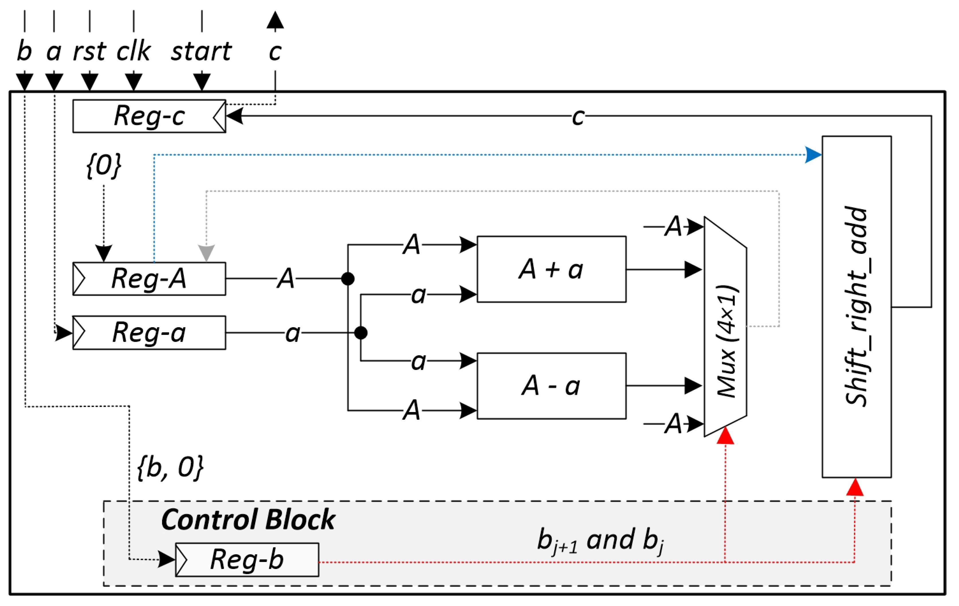
3. Proposed Booth Accelerator Architecture

The architecture of the proposed Booth multiplier design is given in Figure 1. It contains six input/output pins. The input pins are c l k , r s t , s t a r t , a, and b. The corresponding output pin is c. Moreover, the c l k , r s t , and s t a r t inputs are one bit, while the remaining input pins (i.e., a and b) are m bits for m-bit operand lengths. The output pin c’s size is 2m bits. The m-bit operand size ensures that our accelerator is parameterized and flexible. Depending on the user’s choice, it can take different operand sizes as inputs and generate the multiplication result accordingly. We let the reader know that the Booth accelerator only multiplies polynomials without considering polynomial reduction. Therefore, the internal architecture of our proposed Booth accelerator depends on several elements such as three m-bit registers, i.e., Reg-A, Reg-a, Reg-b, and one 2m-bit register, named Reg-c. Moreover, it contains one m-bit adder and subtractor, one 4 × 1 multiplexer, one shift-right-add block, and a control unit. We describe these components one after another in the following text.

3.1. Registers (or Buffers)

As shown in Algorithm 2, the required storage elements are A, b ¯ , and c. It can be seen that lines five and eight of Algorithm 2 require input of polynomial a for completion of the addition and subtraction operations. This is why the proposed accelerator contains four registers: three m bits and one 2m bit. These registers are reused throughout the multiplication process, which allows us to obtain minimum hardware resource utilization. In addition, these four registers are temporary storage elements in our design. We discuss more specific details below.
Reg-A is an accumulator buffer that initializes with 0 at reset, and then, in each clock cycle during the multiplication process, it updates values with the new ones. We preserve the input polynomial a in Reg-a for the corresponding addition and subtraction executions of Algorithm 2. It can be observed that the input polynomial a is only needed for the addition and subtraction operations, and it never updates the corresponding Reg-a during the entire multiplication execution. Therefore, Reg-a can be avoided, but on the other hand, the design faces synchronization issues. Thus, we must hold the input polynomial a in Reg-a to eliminate such problems. The b ¯ storage element of Algorithm 2 is shown with simple Reg-b in Figure 1. Thus, from now on in the manuscript, Reg-b means that it has a value of b ¯ . Reg-b contains a polynomial b with an additional 0-bit next to the least significant bit (LSB) of the multiplier for Booth encoding. Moreover, this Reg-b is a part of the control block that shifts two bits (i.e., b j + 1 and b j ) towards the right in each clock cycle to conduct the multiplication operation. Finally, Reg-c keeps the resultant polynomial of 2m-bit size.

3.2. Adder and Subtractor

The adder and subtractor circuits require two inputs. The first input is from the accumulator, and the other is the polynomial a, which is a multiplicand. We remind the reader that the accumulator is Reg-A and the multiplicand is preserved in Reg-a. Figure 1 confirms the input connections to the adder and subtractor, which are from registers Reg-A and Reg-a. Depending on the values of b j + 1 and b j in each clock cycle, the adder accumulates the multiplicand into Reg-A. If we delve more into it, the adder operates when the inspected bits for b j + 1 and b j are 01. Similarly, the subtractor is responsible for subtracting the multiplicand from the accumulated value preserved in Reg-A. In other words, the subtractor operates when the inspected bits for b j + 1 and b j are 10.
There are several choices or possibilities for implementing the logic for the adder and subtractor. For example, in existing Booth multiplication designs [4,17,18], the most frequently used adder circuit is a carry-save, which efficiently computes the sum of three or more binary numbers. Such adder architectures benefit when implementing optimized variants of a Booth multiplier like radix-2, radix-4, radix-8, and so on. Instead of the carry-save adder, other possible circuits are the carry-lookahead adder, ripple-carry adder, etc. Note that these different adder circuits have their advantages and limitations. We want to let the reader know that subtractor designs can be implemented using adder logic in the digital circuit domain. An adder–subtractor can add and subtract binary numbers in one circuit. However, our accelerator is parameterized and flexible, so we prefer the most straightforward solutions for implementing these circuits. We used the Verilog HDL adder and subtractor operators (+ and −) to enforce these blocks.

3.3. Multiplexer (4 × 1)

The multiplexer is a routing network between the adder, subtractor, and Reg-A. The corresponding inputs to this multiplexer are from the adder, subtractor, and Reg-A. Similarly, its output is also connected to the accumulator register to hold the accumulated result, as shown in Figure 1. The control block will generate the two-bit control signal, shown with red dotted lines in Figure 1, to select the correct input signal for multiplexer output. Whenever a similar control signal to this multiplexer is input, meaning 00 or 11, the multiplexer selects the value from Reg-A—which signals not to do anything and holds the previous value of the Reg-A. For the other two cases, when the two-bit control signal is 01 or 10, the multiplexer selects the output from the adder or subtractor to update the accumulator, respectively.

3.4. Shift-Right-Add Block
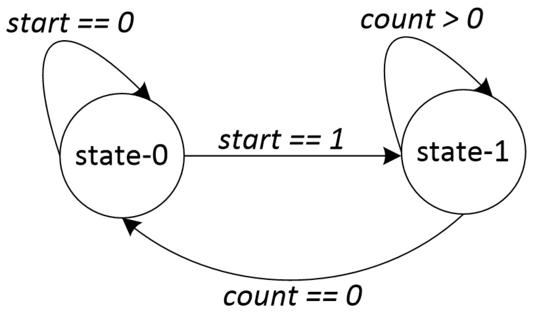
The s h i f t _ r i g h t _ a d d unit in Figure 1 takes three inputs and produces one output. The inputs are b j + 1 , b j , and Reg-A, while the output is the resultant polynomial c. We already mentioned in Section 2.2 that the s h i f t _ r i g h t _ a d d function in lines 6 and 9 of Algorithm 2 facilitates the multiplication of the multiplicand by 2 through the shift and add operations. This means that whenever the values for b j + 1 and b j are 01 or 10, perform a 2-bit shift in Reg-A towards the right, and then, update the corresponding Reg-c. Similarly, whenever the values for b j + 1 and b j are 00 or 11, this means do not do anything and keep Reg-c as its previous value.

3.5. FSM Controller

This work employs an FSM controller to execute control functionalities, as illustrated in Figure 2. The controller’s primary responsibilities include (i) generating control signals for the 4 × 1 routing multiplexer and (ii) inspecting two bits of b j + 1 and b j in one clock cycle from Reg-b. The controller logic is characterized by two states, outlined in Figure 2. We provide some more specific details about these two states below.
The FSM’s initial state is state-0. This is an idle state, which means the multiplier will stay in this state until the s t a r t signal is 1. Moreover, upon reset, it means that when the r s t signal is 1, the FSM of the multiplier design initializes all registers with their default values—whenever the FSM receives a s t a r t signal with 1, it turns to state-1.
State-1 of the FSM ensures the complete polynomial multiplication computation. It starts execution when it receives the s t a r t signal as 1. Moreover, our parameterized multiplier accelerator design uses an additional 12-bit c o u n t register, not previously shown in Figure 1. The reason to use a 12-bit register is to provide flexibility for multiplying polynomials up to 2 12 . This means users can multiply polynomials up to operand lengths of 4096 bits. This is the limitation of our accelerator design. It is possible to increase the size of this c o u n t register, but the implementation results reported in this paper are with a 12-bit c o u n t register. Upon reset, the c o u n t register is initialized with the ratio of the size of the input operands as 2. For example, for an m-bit operand length, the size of the c o u n t register would be m / 2 . Whenever users target input operands with odd values, the c o u n t register is initialized with m + 1 / 2 to make them even. Then, in each clock cycle, when FSM is in state-1, the controller inspects b j + 1 and b j from Reg-b and passes them as a select line to the routing multiplexer. Moreover, the controller also passes b j + 1 and b j to the Shift-right-add block. Additionally, in each clock cycle, when FSM is in state-1, the controller updates the c o u n t register with a decrement of 1. When the value of the c o u n t register becomes 0, FSM shifts its state from state-1 to state-0, which means polynomial multiplication has finished.
Consequently, if we consider the computational cost of our proposed Booth accelerator, it needs m 2 clock cycles for multiplying one m-bit polynomial. The reason is that the traditional Booth multiplier deals with two bits in one clock cycle for multiplying polynomials.
In summary, this section outlines the hardware architecture of the Booth polynomial multiplier, which offers advantages in reducing hardware resource usage (as will be detailed in the upcoming section) with a polynomial multiplication overhead, requiring m 2 clock cycles to implement. It is important to note several polynomial multiplication algorithms from the literature that demand fewer clock cycles, such as Karatsuba [24], Toom–Cook [25,26], and multipliers based on number theoretic transform (NTT) [27,28]. However, it is worth mentioning that the corresponding algorithms for these multiplication methods typically require higher hardware resources. Thus, there is always a trade-off between parameters like clock cycles and hardware resources.

4. Results and Comparison

We provide implementation results and a comparison with state-of-the-art hardware accelerators in Section 4.1 and Section 4.2, respectively.

4.1. Results

Using the Vivado IDE design tool, we implement the proposed Booth accelerator in a Verilog HDL. For different operand lengths, the register-transfer-level (RTL) implementations are verified against the equivalent C/C++-implemented reference design. The hardware-implemented results after the post-place and route are given in Table 1. We used the Xilinx Virtex-7 (xc7vx690tffg1930-3) device for performance evaluations. The targeted operand sizes are presented in j × k format in column one, where j and k show the size of the first and second operands to the multiplier as inputs. Moreover, we targeted different operand sizes: first, in powers of 2, which means we start from 16 × 16 and go up to the maximum operand size of 1024 × 1024; second, in NIST-recommended binary field lengths of 163, 233, 283, 409, and 571; and finally, in the NIST recommended prime field lengths of 192, 224, 256, 384, and 521. The area results in slices, LUTs, and flip-flops (FFs) are provided in column two. The design’s clock cycle utilization and operating frequency are in columns three and four. Column five shows the computation time for one polynomial multiplication in μ s. The computation time is the latency (in μ s), which can be calculated using Equation (2). Finally, the last column shows the power results in milliwatts (mW). Moreover, we point out to the reader that the Vivado tool gives the slices, LUTs, FFs, frequency, and power results reported in Table 1. For clock cycles, it is understood that the traditional Booth multiplier needs m 2 cycles for m-bit polynomial multiplications as it operates two bits in one clock cycle for multiplying m-bit polynomials.
L a t e n c y ( μ s ) = C l o c k C y c l e s ( C C s ) F r e q u e n c y ( i n MHz )

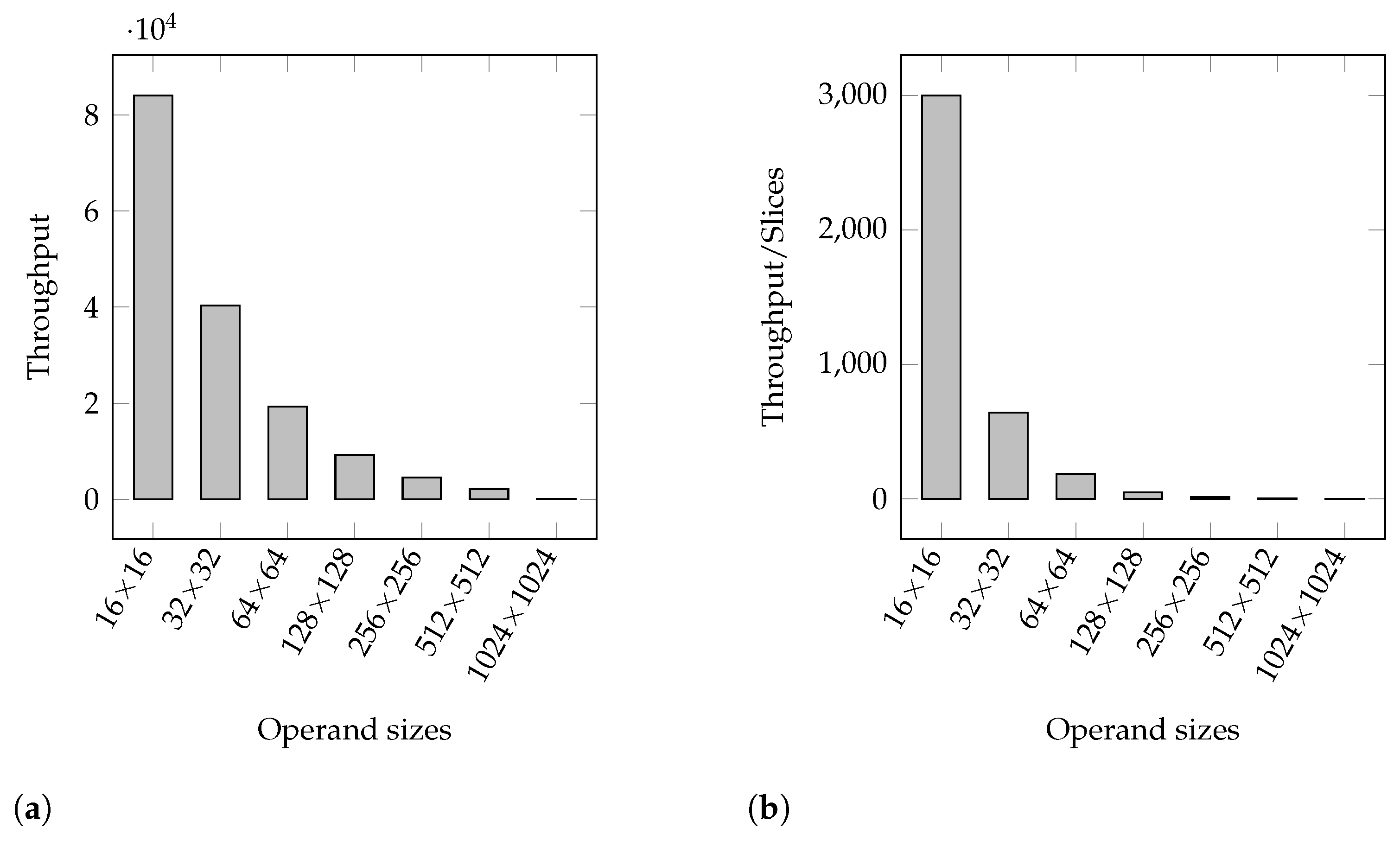
4.1.1. Booth Designs for Operand Sizes in Powers of Two

The trend in powers of 2 shows that with the increase in the operand size from 16 × 16 to 1024 × 1024, there is an increase in the slices, LUTs, and utilized FFs. This is evident in columns two to four of Table 1. The reason behind this is that the implemented Booth multiplier uses the four registers of Reg-A, Reg-a, Reg-b, and Reg-c. Our Booth accelerator is parameterized so that designers can target different operand lengths. Therefore, the increase in the operand sizes also increases the lengths of the four registers in our Booth accelerator and consequently leads to an increase in overall hardware resources. In addition to the hardware resources, column five reveals that when the operand lengths increase, the clock cycles for polynomial multiplication also increase. On the other hand, the operating frequency decreases with the increase in the operand size, as shown in column six of Table 1. As mentioned in this article, latency is a ratio of clock cycles with the circuit frequency; therefore, the increase in the operand size also increases the latency. For example, the required computation time or latency for a 16 × 16 Booth implementation is 0.0119 μ s, while for the maximum considered operand size of 1024 × 1024, this value goes up to 0.9779 μ s. This increase in computation time is 82.17 (ratio of 0.9779 with 0.119) times the 16 × 16-implemented Booth design, and is expected as the operand size also increases. The power consumption of the implemented Booth multiplier also increases with the increase in the operand size, as presented in the last three columns of Table 1.
We provided throughput and throughput/area results of the parameterized Booth multiplier (only for operand sizes of powers of two) in Figure 3a and Figure 3b, respectively. We calculated throughput using Equation (3). Similarly, we computed throughput/area using Equation (4), using slices as area metrics. Note that it is also possible to use LUTs or FFs as an area for evaluation instead of slices. Therefore, Figure 3a,b show an exponential decrease in throughput and throughput/slices with increased operand length. These figures reveal that for shorter operand sizes of 16 × 16 and 32 × 32, the values for throughput and throughput/slices ratio are better with larger operand sizes such as 512 × 512 and 1024 × 1024.
T h r o u g h p u t = 1 L a t e n c y ( μ s ) = 10 6 L a t e n c y
T h r o u g h p u t A r e a = T h r o u g h p u t S l i c e s

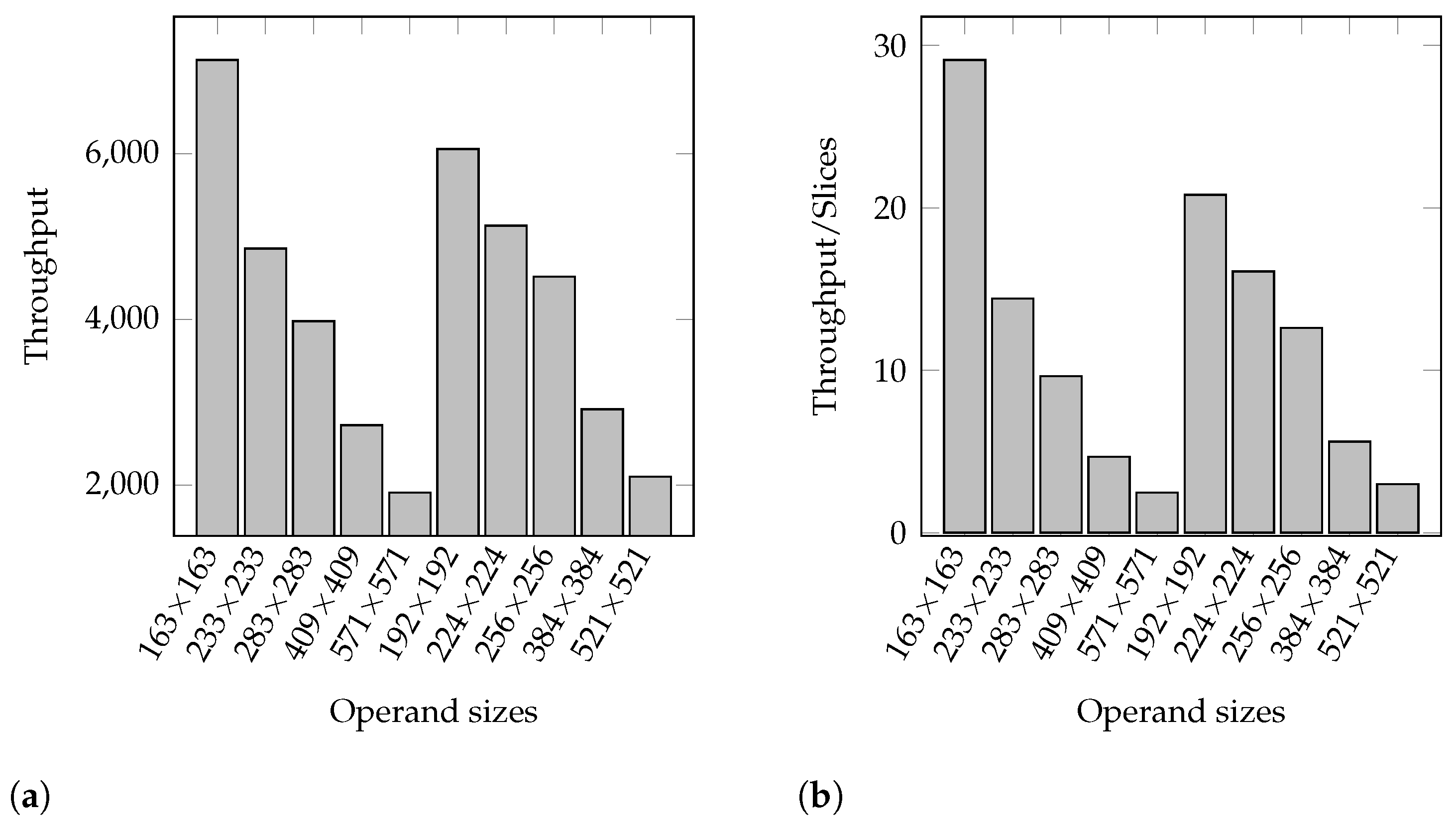
4.1.2. Booth Designs for Operand Sizes Recommended by NIST

If we consider the binary and prime ECC fields recommended by NIST for evaluation, there is an increase in the hardware area in slices, LUTs, and FFs with the rise in the operand size. The area increase can be seen in columns two to four of Table 1. The reported area values benefit the related community in deciding whether to choose our implemented Booth multiplier or not for their choice of application. As expected, the clock cycles, power consumption, and computation time or latency increase with the increase in operand sizes. The operating frequency shows a decrease with the rise in operand length.
Similar to the throughput and throughput/area results from Figure 3a,b, we provide throughput and throughput/slices results for prime and binary ECC fields in Figure 4a,b. The throughput and throughput/area values are calculated using Equation (3) and Equation (4), respectively. Summarizing the findings, it is evident that the increase in operand sizes decreases throughput and the throughput/area ratio. Moreover, these figures show that for shorter operand sizes of 163 × 163 and 192 × 192, the values for throughput and throughput/slices ratio are higher than the larger operand sizes such as 571 × 571 and 521 × 521.

4.1.3. Summary of the Results

Table 1 and Figure 3a,b and Figure 4a,b demonstrate that the increase in operand length increases the hardware area and computation time, while as expected, it decreases the operating frequency. Moreover, our Booth multiplier accelerator with shorter operand lengths is convenient for a wide range of applications, including but not limited to WSNs, RFID, elliptic curves, error-correcting codes, signal-processing algorithms for filtering, convolution, correlation, etc.

4.2. Comparisons

We compare our results with existing hardware implementations of various non-digitized bit-serial polynomial multiplication approaches in Table 2. Column one provides the reference implemented design. The name of the multiplication algorithm or method is shown in column two. We provide the implementation device in column three. The operand length is shown with j × k in column four. Columns five and six give the circuit frequency (in MHz) and latency (in μ s), respectively. The computation time is the latency, which can be calculated using Equation (2). The last column shows the area cost in slices and LUTs. We use “-” in Table 2 where the corresponding information in the reference designs is unavailable.
In comparison to the radix-2 Montgomery-based hardware accelerator of polynomial multiplication of [4], our accelerator on Virtex-6 for an operand size of 1024 × 1024 achieves 71.5 MHz, while this value in the reference design is 53.23 MHz, which is comparatively 1.34 (ratio of 71.5 with 53.23) times lower. Similarly, our accelerator is 1.34 (ratio of 71.5 with 53.23) times faster in computation time (or latency). Instead of the circuit frequency and latency comparison, our accelerator achieves 2429 LUTs while the design of [4] utilizes 2566 LUTs, which is comparatively 1.05 times higher than this work. Probably this is due to the use of a Schoolbook technique for partial product generation in this work.
On the Virtex-5 FPGA, the Montgomery-based polynomial multiplier design of [13] for an operand size of 1024 × 1024 achieves a maximum frequency of 400 MHz, which is comparatively 10.16 (ratio of 400 with 39.35) times higher than the operating frequency achieved in this work (i.e., 39.35 MHz). This higher operating frequency in the reference design of [13] results in a lower computation time than our Booth hardware accelerator, as shown in column six of Table 2. Indeed, our Booth hardware accelerator needs more computation time than the reference design; conversely, our accelerator is more efficient in hardware area cost. Specifically, our design utilizes 4113 slices, while the reference accelerator used 6105 slices on a similar Virtex-5 FPGA.
A programmable-cellular-automata-based bit-serial polynomial multiplier accelerator is implemented on a Virtex-II FPGA in [14]. Virtex-II is a Xilinx family introduced in January 2001 on 150 nm process technology [31]. Xilinx introduced the Virtex-II Pro family in March 2002 on 90 nm process technology [32]. Both these families are considered legacy devices and are not recommended for use in new designs, although Xilinx still produces them for existing designs. The equivalent 90 nm process technology is Virtex-4 [33], which we used to compare our hardware accelerator of the Booth multiplier with the reference implementation of [14]. For an operand size of 163 × 163, the reference design achieves a maximum frequency of 177.8 MHz, while our accelerator runs at 131 MHz. Comparatively, the reference multiplier accelerator is faster in operating frequency than our hardware accelerator. This higher circuit frequency in the reference design results in a lower computation time than our accelerator, evident in column six of Table 2. Similarly, our accelerator uses more slices than the accelerator of [14]. This might happen due to using different devices, i.e., Virtex-II in the reference design and Virtex-4 in our work.
Compared to the Spartan-6 implementation of a 32 × 32 radix-4 Booth multiplier of [17], our Kintex-7 Booth multiplier accelerator is 6.45 (ratio of 645.161 with 100) times faster in operating frequency. One reason could be the different implementation platforms. Another reason is the use of registers/buffers in our accelerator, which benefits in optimizing the frequency, while in the reference accelerator, a combinational logic is implemented. A comparison to the latency is impossible as the reference design lacks this information. Although our accelerator operates at a higher circuit frequency, on the other hand, it utilizes more area in LUTs than the reference design. Thus, there is always a trade-off between frequency and area utilization. The Kintex-7-implemented design in [18] considers 16 × 16 operand lengths. On similar Kintex-7 devices using the same operand sizes, our design uses fewer LUTs than the reference design. The other parameters cannot be compared because the reference design lacks the corresponding details.

5. Conclusions

This article has presented a parameterized hardware accelerator design for the Booth polynomial multiplier. The parameterization enhances flexibility, enabling users to conduct multiplication across diverse operand lengths rather than being restricted to specific operand sizes. We have reused hardware resources to optimize the Booth accelerator efficiently, which helps minimize the design’s overall area cost. Moreover, an FSM-based controller is implemented for control purposes. A detailed comparison of the results (in terms of throughput over area) of the proposed Booth multiplier design with several non-digitized bit-serial polynomial multiplication accelerators is provided. The Booth multiplier design is implemented in Verilog HDL using the Vivado IDE, and the implementation results are considered up to the post-place and route stage on the Xilinx Virtex-7 FPGA. The architecture allows various operand sizes up to 4096 bits for evaluation. Thus, our accelerator with shorter operand lengths is more convenient for various applications.

Funding

This research received no external funding.

Data Availability Statement

The work performed in this study is not available due to security reasons.

Conflicts of Interest

The author declares no conflicts of interest.

References

  1. Imran, M.; Abideen, Z.U.; Pagliarini, S. A Versatile and Flexible Multiplier Generator for Large Integer Polynomials. J. Hardw. Syst. Secur. 2023, 7, 55–71. [Google Scholar] [CrossRef]
  2. Rashid, M.; Imran, M.; Jafri, A.R.; Al-Somani, T.F. Flexible architectures for cryptographic algorithms—A systematic literature review. J. Circuits Syst. Comput. 2019, 28, 1930003. [Google Scholar] [CrossRef]
  3. Imran, M.; Abideen, Z.U.; Pagliarini, S. An Open-source Library of Large Integer Polynomial Multipliers. In Proceedings of the 24th International Symposium on Design and Diagnostics of Electronic Circuits & Systems (DDECS), Vienna, Austria, 7–9 April 2021; pp. 145–150. [Google Scholar] [CrossRef]
  4. Abd-Elkader, A.A.; Rashdan, M.; Hasaneen, E.S.A.; Hamed, H.F. Advanced implementation of Montgomery Modular Multiplier. Microelectron. J. 2020, 106, 104927. [Google Scholar] [CrossRef]
  5. Sajid, A.; Sonbul, O.S.; Rashid, M.; Jafri, A.R.; Arif, M.; Zia, M.Y.I. A Crypto Accelerator of Binary Edward Curves for Securing Low-Resource Embedded Devices. Appl. Sci. 2023, 13, 8633. [Google Scholar] [CrossRef]
  6. Rashid, M.; Sonbul, O.S.; Arif, M.; Qureshi, F.A.; Alotaibi, S.S.; Sinky, M.H. A Flexible Architecture for Cryptographic Applications: ECC and PRESENT. Comput. Mater. Contin 2023, 76, 1009–1025. [Google Scholar] [CrossRef]
  7. Imran, M.; Rashid, M. Architectural review of polynomial bases finite field multipliers over GF(2m). In Proceedings of the International Conference on Communication, Computing and Digital Systems (C-CODE), Islamabad, Pakistan, 8–9 March 2017; pp. 331–336. [Google Scholar] [CrossRef]
  8. Imran, M.; Abideen, Z.U.; Pagliarini, S. An Experimental Study of Building Blocks of Lattice-Based NIST Post-Quantum Cryptographic Algorithms. Electronics 2020, 9, 1953. [Google Scholar] [CrossRef]
  9. Sajid, A.; Sonbul, O.S.; Rashid, M.; Arif, M.; Jaffar, A.Y. An Optimized Hardware Implementation of a Non-Adjacent Form Algorithm Using Radix-4 Multiplier for Binary Edwards Curves. Appl. Sci. 2023, 14, 54. [Google Scholar] [CrossRef]
  10. Rashid, M.; Sonbul, O.S.; Zia, M.Y.I.; Arif, M.; Sajid, A.; Alotaibi, S.S. Throughput/Area-Efficient Accelerator of Elliptic Curve Point Multiplication over GF (2233) on FPGA. Electronics 2023, 12, 3611. [Google Scholar] [CrossRef]
  11. Rashid, M.; Jamal, S.S.; Khan, S.Z.; Alharbi, A.R.; Aljaedi, A.; Imran, M. Elliptic-curve crypto processor for rfid applications. Appl. Sci. 2021, 11, 7079. [Google Scholar] [CrossRef]
  12. Imran, M.; Abideen, Z.U.; Pagliarini, S. TTech-LIB: Center for Hardware Security. 2020. Available online: https://github.com/Centre-for-Hardware-Security/TTech-LIB (accessed on 11 March 2024).
  13. Rezai, A.; Keshavarzi, P. High-Throughput Modular Multiplication and Exponentiation Algorithms Using Multibit-Scan–Multibit-Shift Technique. IEEE Trans. Very Large Scale Integr. (VLSI) Syst. 2015, 23, 1710–1719. [Google Scholar] [CrossRef]
  14. Machhout, M.; Guitouni, Z.; Torki, K.; Khriji, L.; Tourki, R. Coupled FPGA/ASIC Implementation of Elliptic Curve Crypto-Processor. Int. J. Netw. Secur. Its Appl. 2010, 2, 100–112. [Google Scholar] [CrossRef]
  15. Venkatachalam, S.; Lee, H.J.; Ko, S.B. Power Efficient Approximate Booth Multiplier. In Proceedings of the IEEE International Symposium on Circuits and Systems (ISCAS), Florence, Italy, 27–30 May 2018; pp. 1–4. [Google Scholar] [CrossRef]
  16. Boppana, N.V.V.K.; Kommareddy, J.; Ren, S. Low-Cost and High-Performance 8 × 8 Booth Multiplier. Circuits Syst. Signal Process. 2019, 38, 4357–4368. [Google Scholar] [CrossRef]
  17. Shinde, K.; Kureshi, A. Hardware Implementation of Configurable Booth Multiplier on FPGA. In Proceedings of the International Conference on Communication, Computing and Digital Systems (C-CODE), Pune, India, 21 February 2016; pp. 60–63. [Google Scholar]
  18. Cheng, X.; Wang, Y.; Liu, J.; Ding, W.; Lou, H.; Li, P. Booth Encoded Bit-Serial Multiply-Accumulate Units with Improved Area and Energy Efficiencies. Electronics 2023, 12, 2177. [Google Scholar] [CrossRef]
  19. Krishnan T., S.; Chalil, A.; Sreehari, K. VLSI Implementation of Reed Solomon Codes. In Proceedings of the 4th International Conference on Computing Methodologies and Communication (ICCMC), Erode, India, 11–13 March 2020; pp. 280–284. [Google Scholar] [CrossRef]
  20. Tang, N.; Lin, Y. Fast Encoding and Decoding Algorithms for Arbitrary (n, k) Reed-Solomon Codes Over F 2 m . IEEE Commun. Lett. 2020, 24, 716–719. [Google Scholar] [CrossRef]
  21. Mandelbaum, D. On decoding of Reed-Solomon codes. IEEE Trans. Inf. Theory 1971, 17, 707–712. [Google Scholar] [CrossRef]
  22. Bai, S.; Ducas, L.; Kiltz, E.; Lepoint, T.; Lyubashevsky, V.; Schanck, J.M.; Schwabe, P.; Seiler, G.; Stehlé, D. CRYSTALS-Dilithium. Selected for NIST PQC Standardization. 2023. Available online: https://pq-crystals.org/dilithium/ (accessed on 4 March 2024).
  23. Schwabe, P.; Avanzi, R.; Bos, J.; Ducas, L.; Kiltz, E.; Lepoint, T.; Lyubashevsky, V.; Schanck, J.M.; Seiler, G.; Stehle, D. CRYSTALS-KYBER. Proposal to NIST PQC Standardization. 2021. Available online: https://csrc.nist.gov/Projects/post-quantum-cryptography/post-quantum-cryptography-standardization/round-3-submissions (accessed on 9 January 2024).
  24. Karatsuba, A.; Ofman, Y. Multiplication of Multidigit Numbers on Automata. Sov. Phys. Dokl. 1963, 7, 595. [Google Scholar]
  25. Carlet, C.; Sunar, B. (Eds.) Arithmetic of Finite Fields. In Proceedings of the WAIFI 2007—International Workshop on the Arithmetic of Finite Fields, Madrid, Spain, 21–22 June 2007; Lecture Notes in Computer Science. Springer: Berlin/Heidelberg, Germany, 2007; Volume 4547. [Google Scholar]
  26. Dutta, S.; Bhattacharjee, D.; Chattopadhyay, A. Quantum circuits for Toom-Cook multiplication. Phys. Rev. A 2018, 98. [Google Scholar] [CrossRef]
  27. Chung, C.M.M.; Hwang, V.; Kannwischer, M.J.; Seiler, G.; Shih, C.J.; Yang, B.Y. NTT Multiplication for NTT-unfriendly Rings. IACR Trans. Cryptogr. Hardw. Embed. Syst. 2021, 2021, 159–188. [Google Scholar] [CrossRef]
  28. Liang, Z.; Zhao, Y. Number Theoretic Transform and Its Applications in Lattice-based Cryptosystems: A Survey. 2022. Available online: http://xxx.lanl.gov/abs/2211.13546 (accessed on 27 December 2023).
  29. NIST. Recommended Elliptic Curves for Federal Government Use. 1999. Available online: https://csrc.nist.gov/csrc/media/publications/fips/186/2/archive/2000-01-27/documents/fips186-2.pdf (accessed on 9 March 2024).
  30. Hankerson, D.; Menezes, A.J.; Vanstone, S. Guide to Elliptic Curve Cryptography 2004. pp. 1–311. Available online: https://link.springer.com/book/10.1007/b97644 (accessed on 27 July 2023).
  31. Xilinx Inc. Form 10-K, Annual Report, Filing Date 12 June 2001. Available online: http://edgar.secdatabase.com/1862/101287001501165/filing-main.htm (accessed on 3 March 2024).
  32. Xilinx Inc. Form 10-K, Annual Report, Filing Date 17 June 2002. Available online: http://edgar.secdatabase.com/2603/101287002002739/filing-main.htm (accessed on 2 March 2024).
  33. Xilinx Inc. Form 10-K, Annual Report, Filing Date 1 June 2005. Available online: http://edgar.secdatabase.com/669/104746905016238/filing-main.htm (accessed on 2 March 2024).
Figure 1. Proposed Booth accelerator architecture. The red and blue dotted lines are the control signals.
Applsci 14 03323 g001
Figure 2. FSM controller of the parameterized Booth multiplier.
Applsci 14 03323 g002
Figure 3. Throughput and throughput/area results of the Booth multiplier when the operand sizes are in powers of two. (a) Throughput of the Booth design when operand sizes in powers of two. (b) Throughput/slices of the Booth design for operand sizes in powers of two.
Applsci 14 03323 g003
Figure 4. Throughput and throughput/area results of the Booth multiplier for operand sizes of NIST prime and binary ECC fields. (a) Throughput of the Booth design with recommended key lengths by NIST for prime and binary fields in ECC. We selected these key lengths as operand sizes to our Booth multiplier based on [30]. (b) Throughput/slices of the Booth design with recommended key lengths by NIST for prime and binary fields of ECC. We selected these key lengths as operand sizes to our Booth multiplier based on [30].
Applsci 14 03323 g004
Table 1. Results on Xilinx Virtex-7 device. CCs: clock cycles; Freq: operating frequency; Lat: latency or computation time; D and S: dynamic and static powers; TP: total power consumption of the Booth accelerator.
Operand Sizes ( j × k )Area UtilizationTiming DetailsPower Results
Slices/LUTs/FFsCCsFreq
(MHz)
Lat
(μs)
D/S/TP
(mW)
Operand sizes in powers of 2
16 × 1628/70/8286660.01117/323/340
32 × 3263/134/163166450.02430/323/353
64 × 64104/260/323326170.05159/323/382
128 × 128195/522/649645910.108114/324/437
256 × 256358/910/12951285780.221177/324/502
512 × 512624/1819/25842565520.463340/325/666
1024 × 10241434/2602/51675125230.977600/327/927
Key lengths by NIST for use in a binary field ECC (taken from [29])
163 × 163245/584/827825840.140153/324/477
233 × 233337/830/11801175680.205161/324/485
283 × 283413/1010/14321425640.251192/324/516
409 × 409582/1457/20702055580.366275/325/600
571 × 571775/2027/28802865460.523372/326/698
Key lengths by NIST for use in a prime field ECC (taken from [29])
192 × 192291/686/973965810.165184/324/508
224 × 224319/800/11351125740.194154/324/478
256 × 256358/910/12951285780.221177/324/502
384 × 384520/1369/19461925600.342254/325/579
521 × 521700/1853/26332615490.475344/325/669
Table 2. Comparison to existing bit-serial multiplier accelerators. Freq: circuit frequency; Lat: latency or computation time; PCA: programmable cellular automata.
Ref.Implemented AlgorithmPlatformOperand Sizes ( j × k )Freq (MHz)Lat ( μ s)Slices/LUTs
[4]Radix-2 MontgomeryVirtex-61024 × 102453.2319.26-/2566
[13]MontgomeryVirtex-51024 × 10244000.886105/-
[14]PCAVirtex-II163 × 163177.80.91225/-
[17]radix-4 BoothSpartan-632 × 32100--/278
[18]radix-4 BoothKintex-716 × 16---/110
This WorkBoothVirtex-61024 × 102471.514.32-/2429
Virtex-51024 × 102439.3513.014113/-
Virtex-4163 × 1631311.24565/-
Virtex-732 × 32645.1610.024830/323
Kintex-716 × 16678.3580.011730/69
Disclaimer/Publisher’s Note: The statements, opinions and data contained in all publications are solely those of the individual author(s) and contributor(s) and not of MDPI and/or the editor(s). MDPI and/or the editor(s) disclaim responsibility for any injury to people or property resulting from any ideas, methods, instructions or products referred to in the content.

